
2001-2013 Microchip Technology Inc.
DS21669D-page 1
MCP6041/2/3/4
Features
• Low Quiescent Current: 600 nA/amplifier (typical)
• Rail-to-Rail Input/Output
• Gain Bandwidth Product: 14 kHz (typical)
• Wide Supply Voltage Range: 1.4V to 6.0V
• Unity Gain Stable
• Available in Single, Dual, and Quad
• Chip Select (CS) with MCP6043
• Available in 5-lead and 6-lead SOT-23 Packages
• Temperature Ranges:
- Industrial: -40°C to +85°C
- Extended: -40°C to +125°C
Applications
• Toll Booth Tags
• Wearable Products
• Temperature Measurement
• Battery Powered
Design Aids
• SPICE Macro Models
• FilterLab
®
Software
• MAPS (Microchip Advanced Part Selector)
• Analog Demonstration and Evaluation Boards
• Application Notes
Related Devices
• MCP6141/2/3/4: G = +10 Stable Op Amps
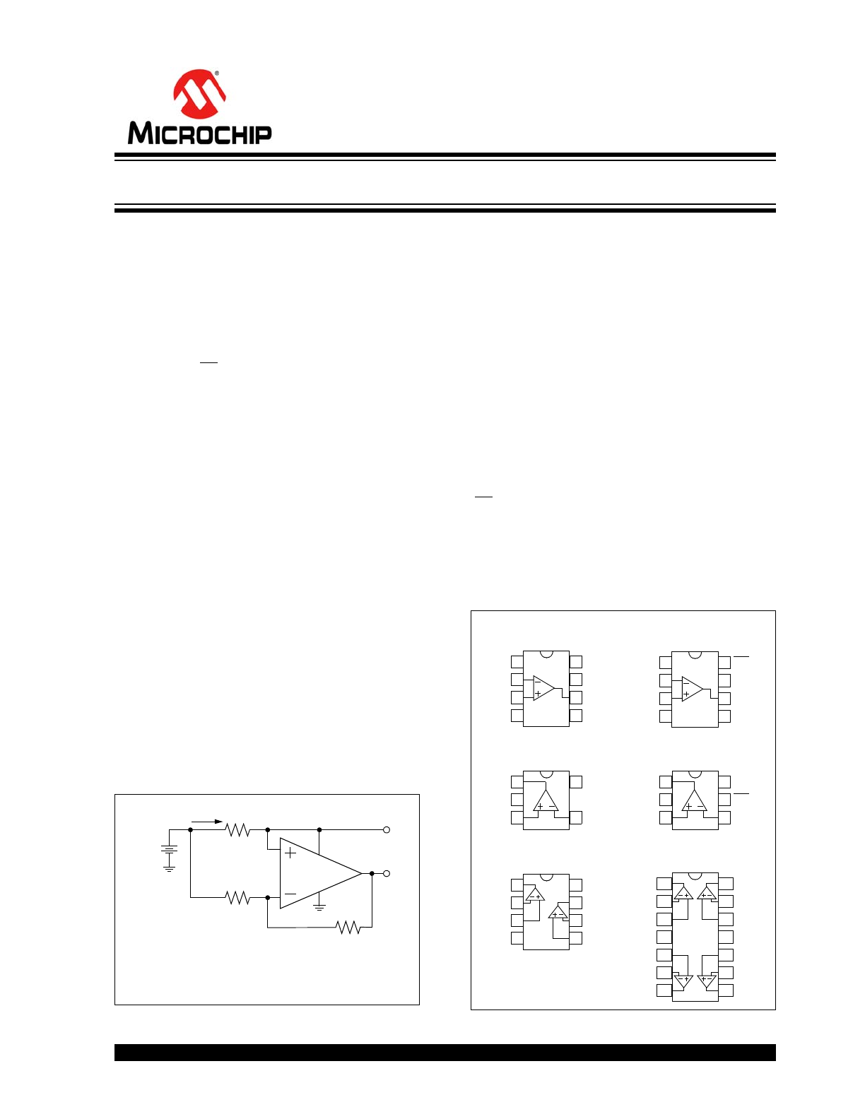
Typical Application
Description
The MCP6041/2/3/4 family of operational amplifiers
(op amps) from Microchip Technology Inc. operate with
a single supply voltage as low as 1.4V, while drawing
less than 1 µA (maximum) of quiescent current per
amplifier. These devices are also designed to support
rail-to-rail input and output operation. This combination
of features supports battery-powered and portable
applications.
The MCP6041/2/3/4 amplifiers have a gain-bandwidth
product of 14 kHz (typical) and are unity gain stable.
These specifications make these op amps appropriate
for low frequency applications, such as battery current
monitoring and sensor conditioning.
The MCP6041/2/3/4 family operational amplifiers are
offered in single (MCP6041), single with Chip Select
(CS) (MCP6043), dual (MCP6042), and quad
(MCP6044) configurations. The MCP6041 device is
available in the 5-lead SOT-23 package, and the
MCP6043 device is available in the 6-lead SOT-23
package.
Package Types
V
DD
I
DD
MCP604X
100 k
1 M
1.4V
V
OUT
High Side Battery Current Sensor
10
to
6.0V
I
DD
V
DD
V
OUT
–
10 V/V
10
------------------------------------------
=
V
IN
+
V
IN
–
V
SS
V
DD
V
OUT
1
2
3
4
8
7
6
5 NC
NC
NC
MCP6041
PDIP, SOIC, MSOP
MCP6042
PDIP, SOIC, MSOP
MCP6043
PDIP, SOIC, MSOP
MCP6044
PDIP, SOIC, TSSOP
V
INA
+
V
INA
–
V
SS
V
OUTB
V
INB
–
1
2
3
4
8
7
6
5 V
INB
+
V
DD
V
OUTA
V
IN
+
V
IN
–
V
SS
V
DD
V
OUT
1
2
3
4
8
7
6
5 NC
CS
NC
V
INA
+
V
INA
–
V
DD
V
IND
–
V
IND
+
1
2
3
4
14
13
12
11 V
SS
V
OUTD
V
OUTA
V
INB
–
V
INB
+
V
OUTB
V
INC
+
V
INC
–
5
6
7
10
9
8 V
OUTC
V
IN
+
V
SS
V
IN
–
1
2
3
5
4
V
DD
V
OUT
MCP6041
SOT-23-5
V
IN
+
V
SS
V
IN
–
1
2
3
6
4
V
DD
V
OUT
MCP6043
SOT-23-6
5 CS
600 nA, Rail-to-Rail Input/Output Op Amps
MCP6041/2/3/4
DS21669D-page 2
2001-2013 Microchip Technology Inc.
1.0
ELECTRICAL
CHARACTERISTICS
Absolute Maximum Ratings †
V
DD
– V
SS
........................................................................7.0V
Current at Input Pins .....................................................±2 mA
Analog Inputs (V
IN
+, V
IN
–) ............. V
SS
– 1.0V to V
DD
+ 1.0V
All Other Inputs and Outputs .......... V
SS
– 0.3V to V
DD
+ 0.3V
Difference Input voltage ...................................... |V
DD
– V
SS
|
Output Short Circuit Current ..................................continuous
Current at Output and Supply Pins ............................±30 mA
Storage Temperature.................................... –65°C to +150°C
Junction Temperature.................................................. +150°C
ESD protection on all pins (HBM; MM)
4 kV; 200V
† Notice: Stresses above those listed under “Absolute
Maximum Ratings” may cause permanent damage to the
device. This is a stress rating only and functional operation of
the device at those or any other conditions above those
indicated in the operational listings of this specification is not
implied. Exposure to maximum rating conditions for extended
periods may affect device reliability.
†† See
Section 4.1 “Rail-to-Rail Input”
DC ELECTRICAL CHARACTERISTICS
Electrical Characteristics: Unless otherwise indicated, V
DD
= +1.4V to +5.5V, V
SS
= GND, T
A
= 25°C, V
CM
= V
DD
/2,
V
OUT
V
DD
/2, V
L
= V
DD
/2, and R
L
= 1 M
to V
L
(refer to
Figure 1-2
and
Figure 1-3
).
Parameters
Sym
Min
Typ
Max
Units
Conditions
Input Offset
Input Offset Voltage
V
OS
-3
—
+3
mV
V
CM
= V
SS
Drift with Temperature
V
OS
/
T
A
—
±2
—
µV/°C
V
CM
= V
SS
, T
A
= -40°C to +85°C
V
OS
/
T
A
—
±15
—
µV/°C
V
CM
= V
SS
,
T
A
= +85°C to +125°C
Power Supply Rejection
PSRR
70
85
—
dB
V
CM
= V
SS
Input Bias Current and Impedance
Input Bias Current
I
B
—
1
—
pA
Industrial Temperature
I
B
—
20
100
pA
T
A
= +85°
Extended Temperature
I
B
—
1200
5000
pA
T
A
= +125°
Input Offset Current
I
OS
—
1
—
pA
Common Mode Input Impedance
Z
CM
—
10
13
||6
—
||pF
Differential Input Impedance
Z
DIFF
—
10
13
||6
—
||pF
Common Mode
Common-Mode Input Range
V
CMR
V
SS
0.3
—
V
DD
+0.3
V
Common-Mode Rejection Ratio
CMRR
62
80
—
dB
V
DD
= 5V, V
CM
= -0.3V to 5.3V
CMRR
60
75
—
dB
V
DD
= 5V, V
CM
= 2.5V to 5.3V
CMRR
60
80
—
dB
V
DD
= 5V, V
CM
= -0.3V to 2.5V
Open-Loop Gain
DC Open-Loop Gain (large signal)
A
OL
95
115
—
dB
R
L
= 50 k
to V
L
,
V
OUT
= 0.1V to V
DD
0.1V
Output
Maximum Output Voltage Swing
V
OL
, V
OH
V
SS
+ 10
—
V
DD
10
mV
R
L
= 50 k
to V
L
,
0.5V input overdrive
Linear Region Output Voltage Swing
V
OVR
V
SS
+ 100
—
V
DD
100
mV
R
L
= 50 k
to V
L
,
A
OL
95 dB
Output Short Circuit Current
I
SC
—
2
—
mA
V
DD
= 1.4V
I
SC
—
20
—
mA
V
DD
= 5.5V
Power Supply
Supply Voltage
V
DD
1.4
—
6.0
V
(
Note 1
)
Quiescent Current per Amplifier
I
Q
0.3
0.6
1.0
µA
I
O
= 0
Note 1: All parts with date codes November 2007 and later have been screened to ensure operation at V
DD
= 6.0V. However,
the other minimum and maximum specifications are measured at 1.4V and/or 5.5V.
2001-2013 Microchip Technology Inc.
DS21669D-page 3
MCP6041/2/3/4
AC ELECTRICAL CHARACTERISTICS
MCP6043 CHIP SELECT (CS) ELECTRICAL CHARACTERISTICS
FIGURE 1-1:
Chip Select (CS) Timing
Diagram (MCP6043 only).
Electrical Characteristics: Unless otherwise indicated, V
DD
= +1.4V to +5.5V, V
SS
= GND, T
A
= 25°C, V
CM
= V
DD
/2,
V
OUT
V
DD
/2, V
L
= V
DD
/2, R
L
= 1 M
to V
L
, and C
L
= 60 pF (refer to
Figure 1-2
and
Figure 1-3
).
Parameters
Sym
Min
Typ
Max
Units
Conditions
AC Response
Gain Bandwidth Product
GBWP
—
14
—
kHz
Slew Rate
SR
—
3.0
—
V/ms
Phase Margin
PM
—
65
—
°
G = +1 V/V
Noise
Input Voltage Noise
E
ni
—
5.0
—
µV
P-P
f = 0.1 Hz to 10 Hz
Input Voltage Noise Density
e
ni
—
170
—
nV/
Hz f = 1 kHz
Input Current Noise Density
i
ni
—
0.6
—
fA/
Hz f = 1 kHz
Electrical Characteristics: Unless otherwise indicated, V
DD
= +1.4V to +5.5V, V
SS
= GND, T
A
= 25°C, V
CM
= V
DD
/2,
V
OUT
V
DD
/2, V
L
= V
DD
/2, R
L
= 1 M
to V
L
, and C
L
= 60 pF (refer to
Figure 1-2
and
Figure 1-3
).
Parameters
Sym
Min
Typ
Max
Units
Conditions
CS Low Specifications
CS Logic Threshold, Low
V
IL
V
SS
—
V
SS
+0.3
V
CS Input Current, Low
I
CSL
—
5
—
pA
CS = V
SS
CS High Specifications
CS Logic Threshold, High
V
IH
V
DD
–0.3
—
V
DD
V
CS Input Current, High
I
CSH
—
5
—
pA
CS = V
DD
CS Input High, GND Current
I
SS
—
-20
—
pA
CS = V
DD
Amplifier Output Leakage, CS High
I
OLEAK
—
20
—
pA
CS = V
DD
Dynamic Specifications
CS Low to Amplifier Output Turn-on Time
t
ON
—
2
50
ms
G = +1V/V, CS = 0.3V to
V
OUT
= 0.9V
DD
/2
CS High to Amplifier Output High-Z
t
OFF
—
10
—
µs
G = +1V/V, CS = V
DD
–0.3V to
V
OUT
= 0.1V
DD
/2
Hysteresis
V
HYST
—
0.6
—
V
V
DD
= 5.0V
V
IL
High-Z
t
ON
V
IH
CS
t
OFF
V
OUT
-20 pA
High-Z
I
SS
I
CS
5 pA
-20 pA
-0.6 µA
(typical)
(typical)
(typical)
(typical)
MCP6041/2/3/4
DS21669D-page 4
2001-2013 Microchip Technology Inc.
TEMPERATURE CHARACTERISTICS
1.1
Test Circuits
The test circuits used for the DC and AC tests are
shown in
Figure 1-2
and
Figure 1-3
. The bypass
capacitors are laid out according to the rules discussed
in
Section 4.6 “Supply Bypass”
.
FIGURE 1-2:
AC and DC Test Circuit for
Most Non-Inverting Gain Conditions.
FIGURE 1-3:
AC and DC Test Circuit for
Most Inverting Gain Conditions.
Electrical Characteristics: Unless otherwise indicated, V
DD
= +1.4V to +5.5V, V
SS
= GND.
Parameters
Sym
Min
Typ
Max Units
Conditions
Temperature Ranges
Specified Temperature Range
T
A
-40
—
+85
°C
Industrial Temperature parts
T
A
-40
—
+125
°C
Extended Temperature parts
Operating Temperature Range
T
A
-40
—
+125
°C
(
Note 1
)
Storage Temperature Range
T
A
-65
—
+150
°C
Thermal Package Resistances
Thermal Resistance, 5L-SOT-23
JA
—
256
—
°C/W
Thermal Resistance, 6L-SOT-23
JA
—
230
—
°C/W
Thermal Resistance, 8L-PDIP
JA
—
85
—
°C/W
Thermal Resistance, 8L-SOIC
JA
—
163
—
°C/W
Thermal Resistance, 8L-MSOP
JA
—
206
—
°C/W
Thermal Resistance, 14L-PDIP
JA
—
70
—
°C/W
Thermal Resistance, 14L-SOIC
JA
—
120
—
°C/W
Thermal Resistance, 14L-TSSOP
JA
—
100
—
°C/W
Note 1:
The MCP6041/2/3/4 family of Industrial Temperature op amps operates over this extended range, but with reduced
performance. In any case, the internal Junction Temperature (T
J
) must not exceed the Absolute Maximum specification
of +150°C.
V
DD
MCP604X
R
G
R
F
R
N
V
OUT
V
IN
V
DD
/2
1 µF
C
L
R
L
V
L
0.1 µF
V
DD
MCP604X
R
G
R
F
R
N
V
OUT
V
DD
/2
V
IN
1 µF
C
L
R
L
V
L
0.1 µF
2001-2013 Microchip Technology Inc.
DS21669D-page 5
MCP6041/2/3/4
2.0
TYPICAL PERFORMANCE CURVES
Note: Unless otherwise indicated, T
A
= +25°C, V
DD
= +1.4V to +6.0V, V
SS
= GND, V
CM
= V
DD
/2, V
OUT
V
DD
/2,
V
L
= V
DD
/2, R
L
= 1 M
to V
L
, and C
L
= 60 pF.
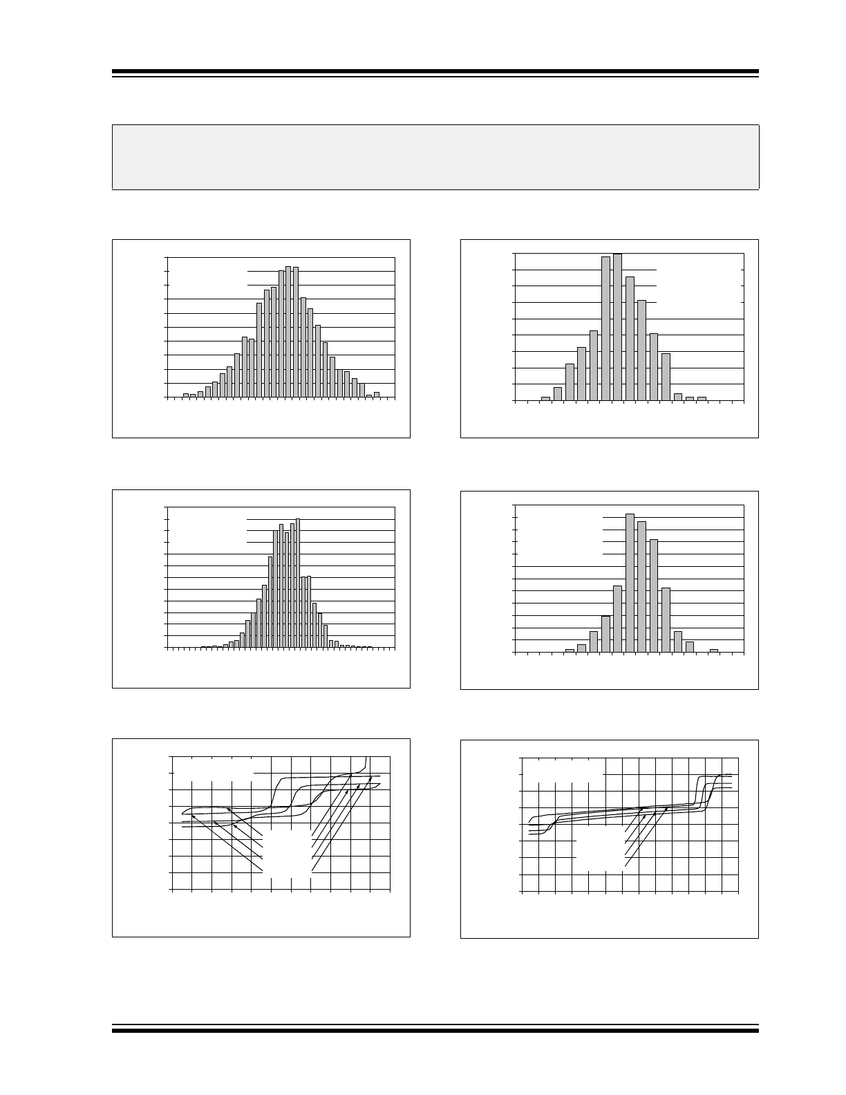
FIGURE 2-1:
Input Offset Voltage.
FIGURE 2-2:
Input Offset Voltage Drift
with T
A
= -40°C to +85°C.
FIGURE 2-3:
Input Offset Voltage vs.
Common Mode Input Voltage with V
DD
= 1.4V.
FIGURE 2-4:
Input Offset Voltage Drift
with T
A
= +85°C to +125°C and V
DD
= 1.4V.
FIGURE 2-5:
Input Offset Voltage Drift
with T
A
= +25°C to +125°C and V
DD
= 5.5V.
FIGURE 2-6:
Input Offset Voltage vs.
Common Mode Input Voltage with V
DD
= 5.5V.
Note:
The graphs and tables provided following this note are a statistical summary based on a limited number of
samples and are provided for informational purposes only. The performance characteristics listed herein are
not tested or guaranteed. In some graphs or tables, the data presented may be outside the specified
operating range (e.g., outside specified power supply range) and therefore outside the warranted range.
0%
1%
2%
3%
4%
5%
6%
7%
8%
9%
10%
-3
-2
-1
0
1
2
3
Input Offset Voltage (mV)
P
er
cent
age of Occur
re
nce
s
1124 Samples
V
DD
= 1.4V and 5.5V
V
CM
= V
SS
0%
1%
2%
3%
4%
5%
6%
7%
8%
9%
10%
11%
12%
-10
-8
-6
-4
-2
0
2
4
6
8
10
Input Offset Voltage Drift (µV/°C)
P
er
c
ent
age of Occu
rr
enc
es
1124 Samples
T
A
= -40°C to +85°C
V
DD
= 1.4V
V
CM
= V
SS
-2000
-1500
-1000
-500
0
500
1000
1500
2000
-0
.4
-0
.2
0.0
0.2
0.4
0.6
0.8
1.0
1.2
1.4
1.6
1.8
Common Mode Input Voltage (V)
Inpu
t O
ffs
et V
o
lt
age
(µ
V
)
V
DD
= 1.4V
Representative Part
T
A
= +125°C
T
A
= +85°C
T
A
= +25°C
T
A
= -40°C
0%
2%
4%
6%
8%
10%
12%
14%
16%
18%
-32 -28 -24 -20 -16 -12
-8
-4
0
4
Input Offset Voltage Drift (µV/°C)
P
e
rce
n
ta
ge
of
Occ
u
rrence
s
245 Samples
1 Representative Lot
T
A
= +85°C to +125°C
V
DD
= 1.4V
V
CM
= V
SS
0%
2%
4%
6%
8%
10%
12%
14%
16%
18%
20%
22%
24%
-32 -28 -24 -20 -16 -12
-8
-4
0
4
Input Offset Voltage Drift (µV/°C)
P
e
rce
n
ta
ge
of
Occ
u
rrence
s
239 Samples
1 Representative Lot
T
A
= +85°C to +125°C
V
DD
= 5.5V
V
CM
= V
SS
-2000
-1500
-1000
-500
0
500
1000
1500
2000
-0
.5
0.0
0.5
1.0
1.5
2.0
2.5
3.0
3.5
4.0
4.5
5.0
5.5
6.0
Common Mode Input Voltage (V)
In
p
u
t Off
set
V
o
lta
g
e (
µ
V
)
V
DD
= 5.5V
Representative Part
T
A
= +125°C
T
A
= +85°C
T
A
= +25°C
T
A
= -40°C
MCP6041/2/3/4
DS21669D-page 6
2001-2013 Microchip Technology Inc.
Note: Unless otherwise indicated, T
A
= +25°C, V
DD
= +1.4V to +6.0V, V
SS
= GND, V
CM
= V
DD
/2, V
OUT
V
DD
/2,
V
L
= V
DD
/2, R
L
= 1 M
to V
L
, and C
L
= 60 pF.
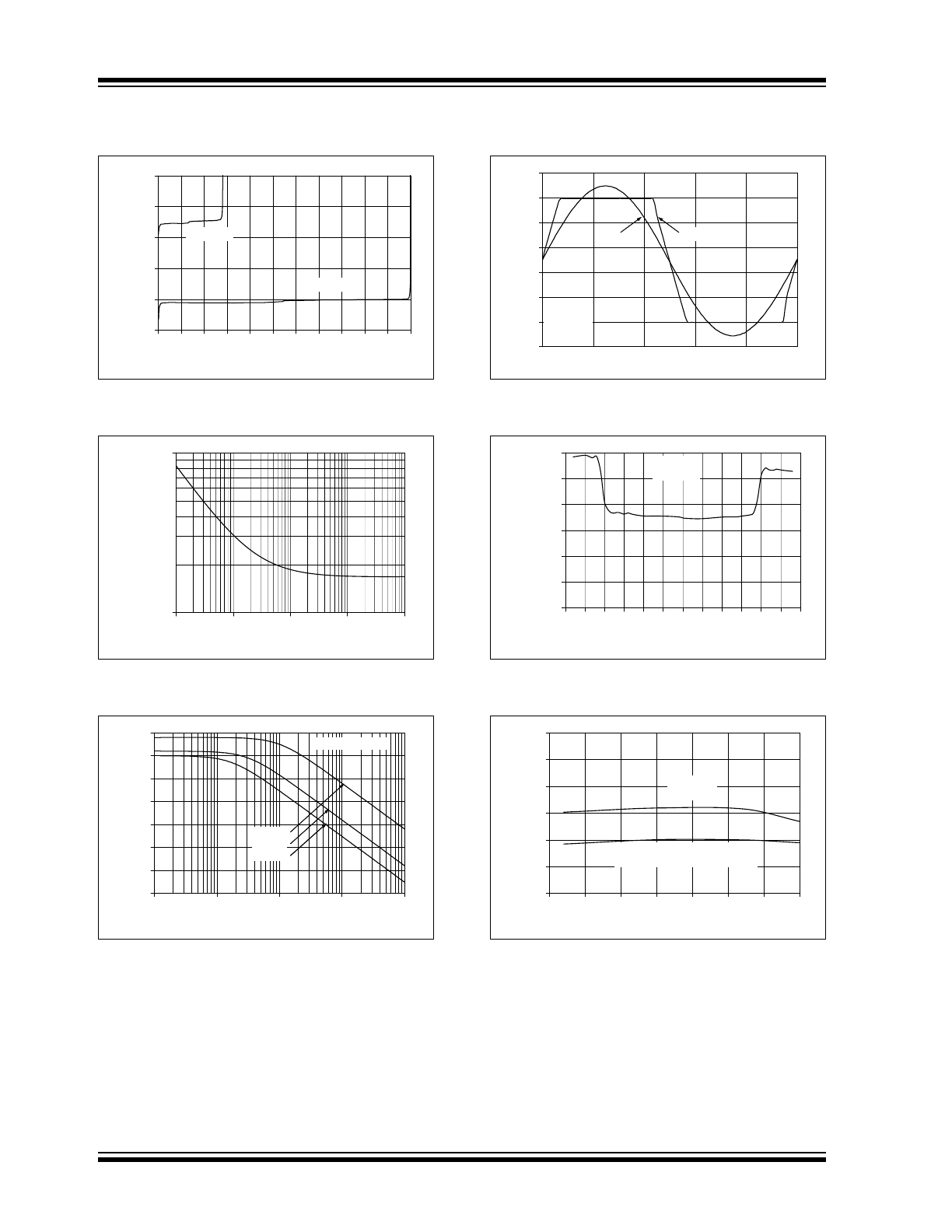
FIGURE 2-7:
Input Offset Voltage vs.
Output Voltage.
FIGURE 2-8:
Input Noise Voltage Density
vs. Frequency.
FIGURE 2-9:
CMRR, PSRR vs.
Frequency.
FIGURE 2-10:
The MCP6041/2/3/4 family
shows no phase reversal.
FIGURE 2-11:
Input Noise Voltage Density
vs. Common Mode Input Voltage.
FIGURE 2-12:
CMRR, PSRR vs. Ambient
Temperature.
250
300
350
400
450
500
0.0 0.5 1.0 1.5 2.0 2.5 3.0 3.5 4.0 4.5 5.0 5.5
Output Voltage (V)
Inp
u
t
Off
set V
o
lt
ag
e (µ
V
)
V
DD
= 5.5V
V
DD
= 1.4V
100
1000
0.1
1
10
100
1000
Frequency (Hz)
Input Noise Voltage Density
(nV/Hz)
20
30
40
50
60
70
80
90
0.1
1
10
100
1000
Frequency (Hz)
CM
RR, PSRR
(
d
B)
PSRR–
PSRR+
CMRR
Referred to Input
-1
0
1
2
3
4
5
6
0
5
10
15
20
25
Time (5 ms/div)
In
p
u
t, Ou
tp
u
t V
o
ltag
es (
V
)
V
IN
V
DD
= 5.0V
G = +2 V/V
V
OUT
0
50
100
150
200
250
300
-0.5
0.0
0.5
1.0
1.5
2.0
2.5
3.0
3.5
4.0
4.5
5.0
5.5
Common Mode Input Voltage (V)
Input Noise Voltage Density
(nV/
Hz)
f = 1 kHz
V
DD
= 5.0V
70
75
80
85
90
95
100
-50
-25
0
25
50
75
100
125
Ambient Temperature (°C)
P
S
RR, CM
RR (
d
B)
PSRR
(V
CM
= V
SS
)
CMRR
(V
DD
= 5.0V, V
CM
= -0.3V to +5.3V)
2001-2013 Microchip Technology Inc.
DS21669D-page 7
MCP6041/2/3/4
Note: Unless otherwise indicated, T
A
= +25°C, V
DD
= +1.4V to +6.0V, V
SS
= GND, V
CM
= V
DD
/2, V
OUT
V
DD
/2,
V
L
= V
DD
/2, R
L
= 1 M
to V
L
, and C
L
= 60 pF.
FIGURE 2-13:
Input Bias, Offset Currents
vs. Ambient Temperature.
FIGURE 2-14:
Open-Loop Gain, Phase vs.
Frequency.
FIGURE 2-15:
DC Open-Loop Gain vs.
Power Supply Voltage.
FIGURE 2-16:
Input Bias, Offset Currents
vs. Common Mode Input Voltage.
FIGURE 2-17:
DC Open-Loop Gain vs.
Load Resistance.
FIGURE 2-18:
DC Open-Loop Gain vs.
Output Voltage Headroom.
0.1
1
10
100
1000
10000
45
55
65
75
85
95
105 115 125
Ambient Temperature (°C)
In
put
B
ias and
Off
set C
u
rr
ents
(p
A
)
| I
OS
|
I
B
V
DD
= 5.5V
V
CM
= V
DD
0.1
1
10
100
1k
10k
-20
0
20
40
60
80
100
120
1.E-
03
1.E-
02
1.E-
01
1.E+
00
1.E+
01
1.E+
02
1.E+
03
1.E+
04
1.E+
05
Frequency (Hz)
O
p
en-
Loo
p G
ai
n
(dB
)
-210
-180
-150
-120
-90
-60
-30
0
Op
en-L
oop
P
h
ase (
°)
0.001 0.01 0.1
1
10 100 1k 10k 100k
Gain
Phase
80
90
100
110
120
130
140
1.0
1.5
2.0
2.5
3.0
3.5
4.0
4.5
5.0
5.5
Power Supply Voltage (V)
DC Op
en
-L
o
o
p
Ga
in
(
d
B)
R
L
= 50 kΩ
V
DD
= 5.0V
V
OUT
= 0.1V to V
DD
- 0.1V
0.1
1
10
100
1000
10000
0.0 0.5 1.0 1.5 2.0 2.5 3.0 3.5 4.0 4.5 5.0 5.5
Common Mode Input Voltage (V)
In
pu
t B
ias an
d Of
fset
C
u
rr
ent
s
(p
A
)
V
DD
= 5.5V
| I
OS
|
I
B
0.1
1
10
100
1k
10k
T
A
= +125°C
T
A
= +85°C
60
70
80
90
100
110
120
130
1.E+02
1.E+03
1.E+04
1.E+05
Load Resistance (
:)
DC Open-Loop Gain (dB)
V
DD
= 1.4V
100
1k
10k
100k
V
OUT
= 0.1V to V
DD
– 0.1V
V
DD
= 5.5V
80
90
100
110
120
130
140
0.00
0.05
0.10
0.15
0.20
0.25
Output Voltage Headroom;
V
DD
V
OH
or V
OL
V
SS
(V)
DC Open-Loop Gain (dB)
R
L
= 50 k
V
DD
= 5.5V
V
DD
= 1.4V
MCP6041/2/3/4
DS21669D-page 8
2001-2013 Microchip Technology Inc.
Note: Unless otherwise indicated, T
A
= +25°C, V
DD
= +1.4V to +6.0V, V
SS
= GND, V
CM
= V
DD
/2, V
OUT
V
DD
/2,
V
L
= V
DD
/2, R
L
= 1 M
to V
L
, and C
L
= 60 pF.
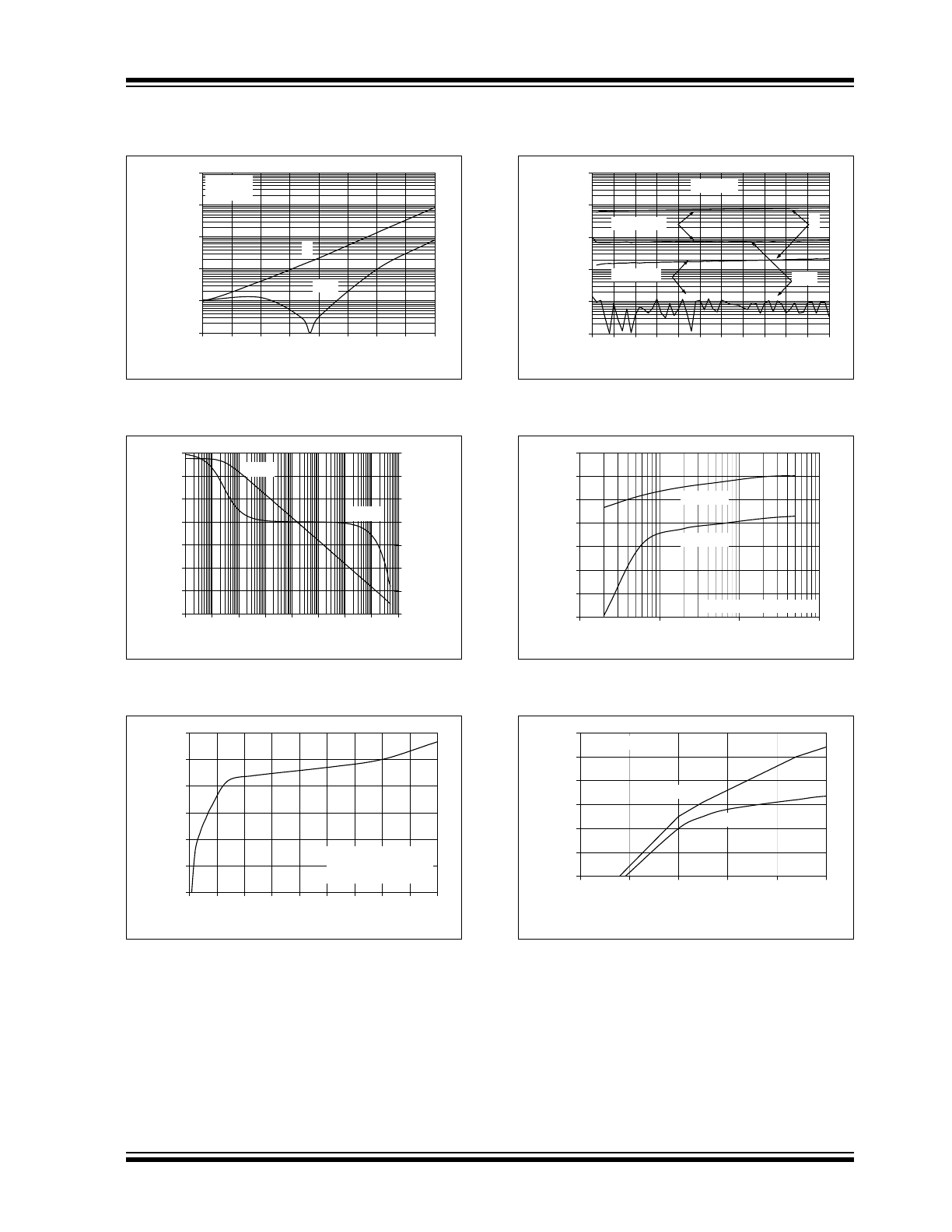
FIGURE 2-19:
Channel-to-Channel
Separation vs. Frequency (MCP6042 and
MCP6044 only).
FIGURE 2-20:
Gain Bandwidth Product,
Phase Margin vs. Ambient Temperature with
V
DD
= 1.4V.
FIGURE 2-21:
Quiescent Current vs.
Power Supply Voltage.
FIGURE 2-22:
Gain Bandwidth Product,
Phase Margin vs. Common Mode Input Voltage.
FIGURE 2-23:
Gain Bandwidth Product,
Phase Margin vs. Ambient Temperature with
V
DD
= 5.5V.
FIGURE 2-24:
Output Short Circuit Current
vs. Power Supply Voltage.
60
70
80
90
100
110
120
130
1.E+02
1.E+03
1.E+04
Frequency (Hz)
Ch
an
n
el t
o
Ch
a
n
n
el
S
epa
ra
ti
on
(d
B
)
100
1k
10k
Input Referred
0
2
4
6
8
10
12
14
16
18
-50
-25
0
25
50
75
100
125
Ambient Temperature (°C)
G
a
in
B
an
d
w
id
th
Pr
odu
ct
(k
H
z)
0
10
20
30
40
50
60
70
80
90
P
h
ase
Mar
g
in
(
°)
PM
(G = +1)
GBWP
V
DD
= 1.4V
0.0
0.1
0.2
0.3
0.4
0.5
0.6
0.7
0.8
0.0 0.5 1.0 1.5 2.0 2.5 3.0 3.5 4.0 4.5 5.0 5.5
Power Supply Voltage (V)
Quie
scent
C
u
rr
e
n
t
(µ
A/Am
p
lif
ier
)
T
A
= +125°C
T
A
= +85°C
T
A
= +25°C
T
A
= -40°C
0
2
4
6
8
10
12
14
16
18
20
-0
.5
0.0
0.5
1.0
1.5
2.0
2.5
3.0
3.5
4.0
4.5
5.0
5.5
Common Mode Input Voltage
Gain
Ban
d
w
id
th
P
ro
d
u
c
t
(kH
z)
0
10
20
30
40
50
60
70
80
90
100
P
h
ase M
ar
g
in
(°)
PM
(G = +1)
GBWP
V
DD
= 5.0V
R
L
= 100 kΩ
0
2
4
6
8
10
12
14
16
18
-50
-25
0
25
50
75
100
125
Ambient Temperature (°C)
G
a
in
B
an
d
w
idt
h
P
ro
d
uc
t
(kH
z)
0
10
20
30
40
50
60
70
80
90
P
h
a
se M
ar
g
in
(°)
PM
(G = +1)
GBWP
V
DD
= 5.5V
0
5
10
15
20
25
30
35
0.0 0.5 1.0 1.5 2.0 2.5 3.0 3.5 4.0 4.5 5.0 5.5
Power Supply Voltage (V)
O
u
tput
Sh
or
t C
ir
cui
t C
u
rr
ent
Ma
gni
tud
e (m
A
)
T
A
= -40°C
T
A
= +25°C
T
A
= +85°C
T
A
= +125°C
2001-2013 Microchip Technology Inc.
DS21669D-page 9
MCP6041/2/3/4
Note: Unless otherwise indicated, T
A
= +25°C, V
DD
= +1.4V to +6.0V, V
SS
= GND, V
CM
= V
DD
/2, V
OUT
V
DD
/2,
V
L
= V
DD
/2, R
L
= 1 M
to V
L
, and C
L
= 60 pF.
FIGURE 2-25:
Output Voltage Headroom
vs. Output Current Magnitude.
FIGURE 2-26:
Slew Rate vs. Ambient
Temperature.
FIGURE 2-27:
Small Signal Non-inverting
Pulse Response.
FIGURE 2-28:
Output Voltage Headroom
vs. Ambient Temperature.
FIGURE 2-29:
Maximum Output Voltage
Swing vs. Frequency.
FIGURE 2-30:
Small Signal Inverting Pulse
Response.
1
10
100
1000
0.01
0.1
1
10
Output Current Magnitude (mA)
Ou
tpu
t V
o
lt
age
H
eadr
o
o
m
;
V
DD
– V
OH
or
V
OL
–
V
SS
(m
V
)
V
DD
– V
OH
V
OL
– V
SS
0.0
0.5
1.0
1.5
2.0
2.5
3.0
3.5
4.0
4.5
5.0
5.5
-50
-25
0
25
50
75
100
125
Ambient Temperature (°C)
S
lew
R
ate
(V
/ms)
High-to-Low
Low-to-High
V
DD
= 1.4V
V
DD
= 5.5V
-25
-20
-15
-10
-5
0
5
10
15
20
25
0.0
0.1
0.2
0.3
0.4
0.5
0.6
0.7
0.8
0.9
1.0
Time (100 µs/div)
Ou
tp
ut V
o
lt
ag
e
(5
m
V
/div
)
G = +1 V/V
R
L
= 50 kΩ
0.0
0.5
1.0
1.5
2.0
2.5
3.0
3.5
4.0
4.5
5.0
-50
-25
0
25
50
75
100
125
Ambient Temperature (°C)
Ou
tpu
t V
o
lt
age
H
e
adr
o
om
,
V
DD
–
V
OH
or
V
OL
–
V
SS
(m
V
)
V
OL
– V
SS
V
DD
– V
OH
V
DD
= 5.5V
R
L
= 50 kΩ
0.1
1
10
1.E+01
1.E+02
1.E+03
1.E+04
Frequency (Hz)
Maxi
m
u
m
O
u
tp
ut
V
o
ltag
e
Sw
in
g (
V
P-
P
)
10
100
1k
10k
V
DD
= 5.5V
V
DD
= 1.4V
-25
-20
-15
-10
-5
0
5
10
15
20
25
0.0
0.1
0.2
0.3
0.4
0.5
0.6
0.7
0.8
0.9
1.0
Time (100 µs/div)
V
o
lt
ag
e (
5
m
V
/d
iv
)
G = -1 V/V
R
L
= 50 kΩ
MCP6041/2/3/4
DS21669D-page 10
2001-2013 Microchip Technology Inc.
Note: Unless otherwise indicated, T
A
= +25°C, V
DD
= +1.4V to +6.0V, V
SS
= GND, V
CM
= V
DD
/2, V
OUT
V
DD
/2,
V
L
= V
DD
/2, R
L
= 1 M
to V
L
, and C
L
= 60 pF.
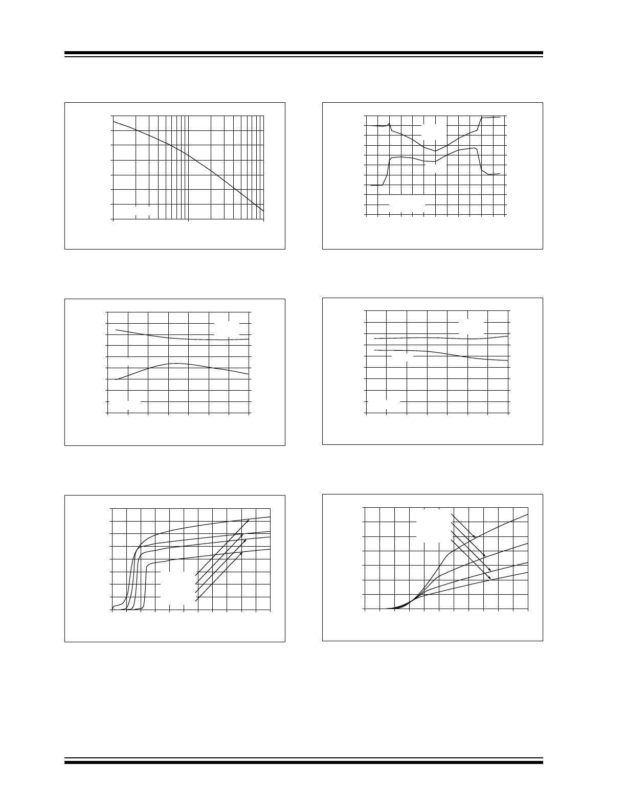
FIGURE 2-31:
Large Signal Non-inverting
Pulse Response.
FIGURE 2-32:
Chip Select (CS) to
Amplifier Output Response Time (MCP6043
only).
FIGURE 2-33:
Input Current vs. Input
Voltage (below V
SS
).
FIGURE 2-34:
Large Signal Inverting Pulse
Response.
FIGURE 2-35:
Chip Select (CS) Hysteresis
(MCP6043 only).
0.0
0.5
1.0
1.5
2.0
2.5
3.0
3.5
4.0
4.5
5.0
0
1
2
3
4
5
6
7
8
9
10
Time (1 ms/div)
Out
p
ut
V
o
lt
age
(V
)
V
DD
= 5.0V
G = +1 V/V
R
L
= 50 kΩ
-20.0
-17.5
-15.0
-12.5
-10.0
-7.5
-5.0
-2.5
0.0
2.5
5.0
7.5
0
1
2
3
4
5
6
7
8
9 10
Time (1 ms/div)
C
S
V
o
lt
ag
e
(V
)
-0.5
0.0
0.5
1.0
1.5
2.0
2.5
3.0
3.5
4.0
4.5
5.0
Ou
tpu
t V
o
lt
age
(V
)
V
DD
= 5.0V
V
OUT
High-Z
High-Z
Output On
CS
1.E-12
1.E-11
1.E-10
1.E-09
1.E-08
1.E-07
1.E-06
1.E-05
1.E-04
1.E-03
1.E-02
-1.0 -0.9 -0.8 -0.7 -0.6 -0.5 -0.4 -0.3 -0.2 -0.1 0.0
Input Voltage (V)
Inpu
t
C
u
rr
ent Mag
n
it
ude (A
)
+125°C
+85°C
+25°C
-40°C
10m
1m
100µ
10µ
1µ
100n
10n
1n
100p
10p
1p
0.0
0.5
1.0
1.5
2.0
2.5
3.0
3.5
4.0
4.5
5.0
0
1
2
3
4
5
6
7
8
9
10
Time (1 ms/div)
Ou
tp
ut V
o
lt
ag
e
(V
)
V
DD
= 5.0V
G = -1 V/V
R
L
= 50 kΩ
-0.5
0.0
0.5
1.0
1.5
2.0
2.5
3.0
0.0 0.5 1.0 1.5 2.0 2.5 3.0 3.5 4.0 4.5 5.0
CS Input Voltage (V)
In
te
rn
al
C
S
S
w
itc
h
Ou
tp
u
t (
V
)
V
OUT
Active
V
OUT
High-Z
V
DD
= 5.0V
Hysteresis
CS
High-to-Low
CS
Low-to-High