
2015 Microchip Technology Inc.
DS20005466A-page 1
MCP48FVBXX
Features
• Operating Voltage Range:
- 2.7V to 5.5V - full specifications
- 1.8V to 2.7V - reduced device specifications
• Output Voltage Resolutions:
- 8-bit: MCP48FVB0X (256 Steps)
- 10-bit: MCP48FVB1X (1024 Steps)
- 12-bit: MCP48FVB2X (4096 Steps)
• Rail-to-Rail Output
• Fast Settling Time of 7.8 µs (typical)
• DAC Voltage Reference Source Options:
- Device V
DD
- External V
REF
pin (buffered or unbuffered)
- Internal Band Gap (1.22V typical)
• Output Gain Options:
- Unity (1x)
- 2x
• Power-on/Brown-out Reset Protection
• Power-Down Modes:
- Disconnects output buffer (High Impedance)
- Selection of V
OUT
pull-down resistors
(100 k
or 1 k)
• Low Power Consumption:
- Normal operation: <180 µA (Single),
380 µA (Dual)
- Power-down operation: 650 nA typical
• SPI Interface:
- Supports ‘00’ and ‘11’ modes
- Up to 20 MHz writes and 10 MHz reads
- Input buffers support interfacing to
low-voltage digital devices
• Package Types: 10-lead MSOP
• Extended Temperature Range: -40°C to +125°C
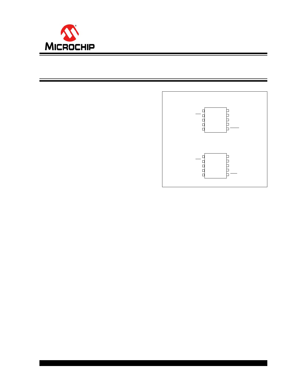
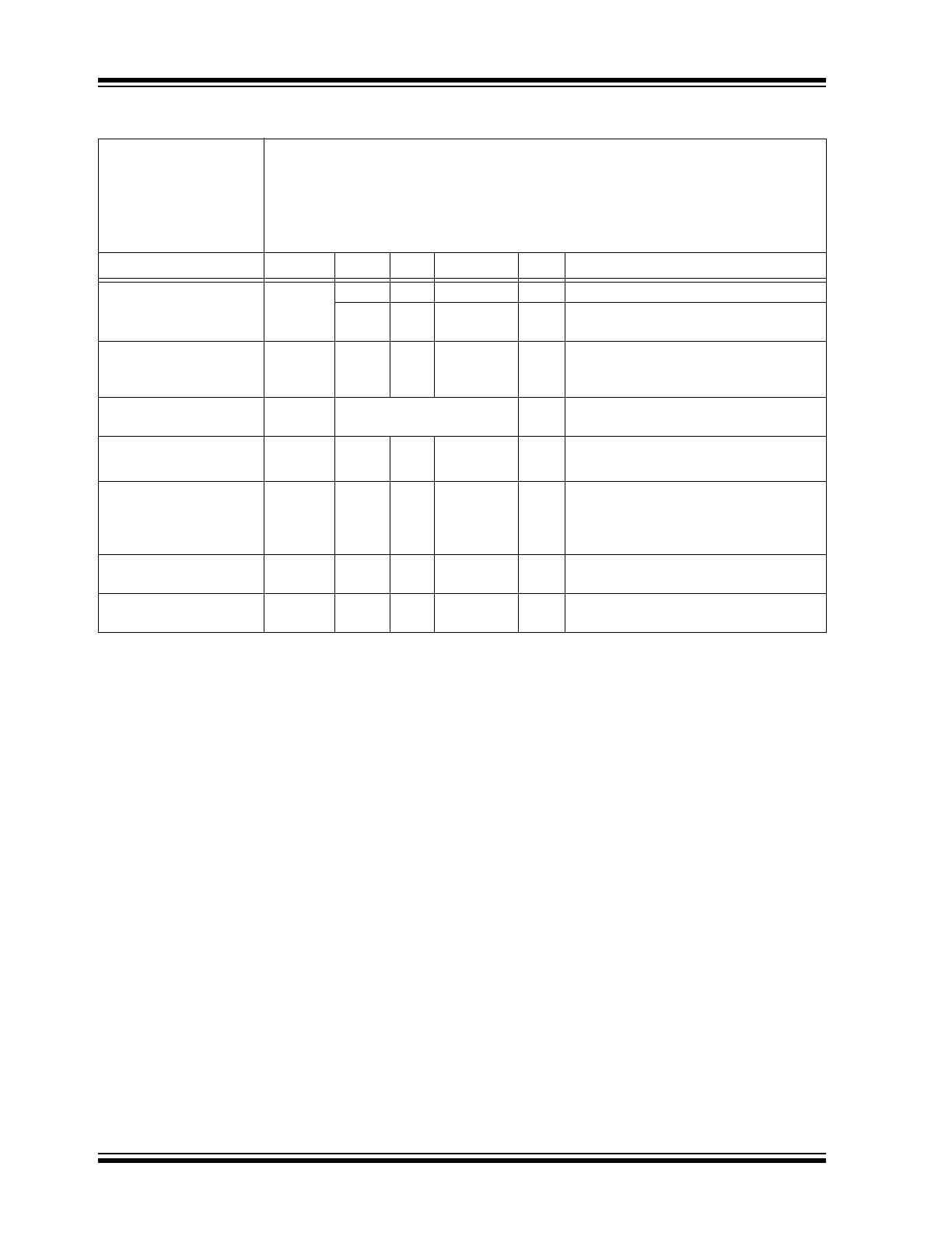
Package Types
General Description
The MCP48FVBXX are Single- and Dual-channel 8-bit,
10-bit, and 12-bit buffered voltage output
Digital-to-Analog Converters (DAC) with volatile
memory and an SPI serial interface.
The V
REF
pin, the device V
DD
or the internal band gap
voltage can be selected as the DAC’s reference
voltage. When V
DD
is selected, V
DD
is connected
internally to the DAC reference circuit. When the V
REF
pin is used, the user can select the output buffer’s gain
to be 1 or 2. When the gain is 2, the V
REF
pin voltage
should be limited to a maximum of V
DD
/2.
These devices have an SPI-compatible serial interface.
Write commands are supported up to 20 MHz while
read commands are supported up to 10 MHz.
Applications
• Set Point or Offset Trimming
• Sensor Calibration
• Low-Power Portable Instrumentation
• PC Peripherals
• Data Acquisition Systems
• Motor Control
Dual
Single
MCP48FVBX2
MSOP
MCP48FVBX1
1
2
3
4
7
8
9
10
V
SS
V
OUT0
V
REF0
CS
V
DD
SCK
SDI
SDO
5
6
LAT0/HVC
NC
MSOP
1
2
3
4
7
8
9
10
V
SS
V
OUT0
CS
V
DD
SCK
SDI
SDO
5
6
V
OUT1
Note 1:
Associated with both DAC0 and DAC1
V
REF
(
1
)
LAT/HVC
(
1
)
8-/10-/12-Bit Single/Dual Voltage Output Volatile
Digital-to-Analog Converters with SPI Interface
MCP48FVBXX
DS20005466A-page 2
2015 Microchip Technology Inc.
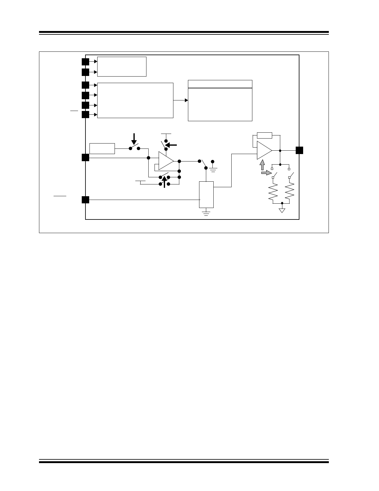
MCP48FVBX1 Device Block Diagram (Single-Channel Output)
Power-up/
Brown-out Control
V
DD
V
SS
SPI Serial Interface Module
Memory (32x16)
DAC0 (Vol)
V
REF0
Op
Amp
Gain
V
OUT0
LAT0/HVC
Re
si
st
o
r
La
dde
r
V
SS
PD1:PD0 and
VREF1:VREF0
VREF1:VREF0
+
-
V
DD
SDI
SDO
Band Gap
(1.22V)
PD1:PD0
VREF1:VREF0
V
DD
V
BG
PD1:PD0
1k
100
k
VREF (Vol)
Power-down (Vol)
Gain (Vol)
Status (Vol)
and PD1:PD0
Note 1:
If Internal Band Gap is selected, this buffer has a 2x gain. If the G bit = ‘1’, this is a total gain of 4.
SCK
CS
and
Control Logic
(
1
)
2015 Microchip Technology Inc.
DS20005466A-page 3
MCP48FVBXX
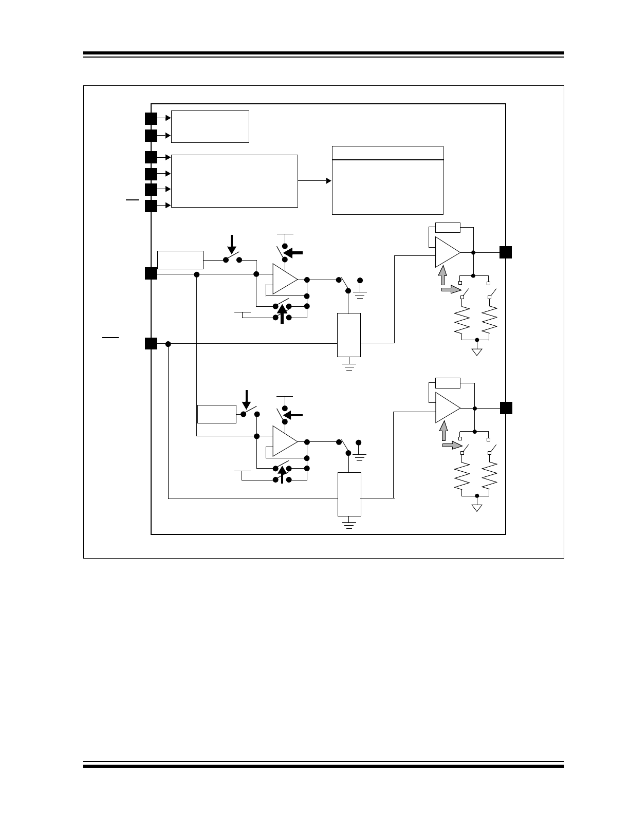
MCP48FVBX2 Device Block Diagram (Dual-Channel Output)
Power-up/
Brown-out Control
V
DD
V
SS
SPI Serial Interface Module
V
REF
LAT/HVC
R
e
si
st
or
Lad
der
Op
Amp
Gain
V
OUT1
Re
si
st
o
r
La
dd
er
intVR1
PD1:PD0 and
VREF1:VREF0
VREF1:VREF0
+
-
V
DD
PD1:PD0 and
VREF1:VREF0
VREF1:VREF0
+
-
V
DD
SDI
SDO
Band Gap
(1.22V)
Band Gap
(1.22V)
PD1:PD0
V
DD
V
BG
V
DD
V
SS
V
SS
PD1:PD0
Op
Amp
Gain
V
OUT0
1k
10
0
k
1k
10
0
k
Memory (32x16)
DAC0 and DAC1 (Vol)
VREF (Vol)
Power-down (Vol)
Gain (Vol)
Status (Vol)
VREF1:VREF0
and PD1:PD0
VREF1:VREF0
and PD1:PD0
PD1:PD0
PD1:PD0
Note 1:
If Internal Band Gap is selected, this buffer has a 2x gain, if the G bit = ‘1’, this is a total gain of 4.
SCK
CS
and
Control Logic
(
1
)
(
1
)
MCP48FVBXX
DS20005466A-page 4
2015 Microchip Technology Inc.
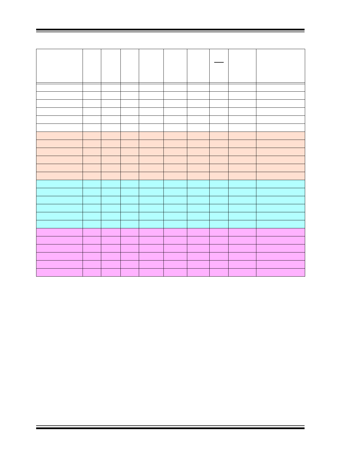
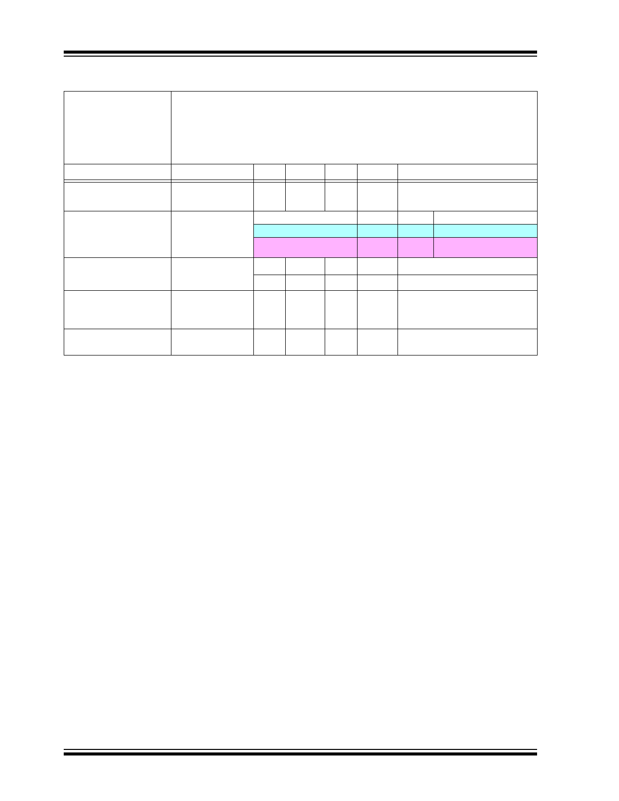
Device Features
Device
# o
f
Cha
n
ne
ls
Re
s
o
lutio
n
(bit
s
)
Con
trol
In
terfac
e
DAC Outp
ut
POR/BOR
Se
tting
(
1
)
# of
V
REF
Inputs
Internal
band
gap ?
# of
LAT
Inputs
Memory
Specified
Operating Range
(V
DD
)
(
2
)
MCP48FVB01
1
8
SPI
7Fh
1
Yes
1
RAM
1.8V to 5.5V
MCP48FVB11
1
10
SPI
1FFh
1
Yes
1
RAM
1.8V to 5.5V
MCP48FVB21
1
12
SPI
7FFh
1
Yes
1
RAM
1.8V to 5.5V
MCP48FVB02
2
8
SPI
7Fh
1
Yes
1
RAM
1.8V to 5.5V
MCP48FVB12
2
10
SPI
1FFh
1
Yes
1
RAM
1.8V to 5.5V
MCP48FVB22
2
12
SPI
7FFh
1
Yes
1
RAM
1.8V to 5.5V
MCP48FEB01
1
8
SPI
7Fh
1
Yes
1
EEPROM
1.8V to 5.5V
MCP48FEB11
1
10
SPI
1FFh
1
Yes
1
EEPROM
1.8V to 5.5V
MCP48FEB21
1
12
SPI
7FFh
1
Yes
1
EEPROM
1.8V to 5.5V
MCP48FEB02
2
8
SPI
7Fh
1
Yes
1
EEPROM
1.8V to 5.5V
MCP48FEB12
2
10
SPI
1FFh
1
Yes
1
EEPROM
1.8V to 5.5V
MCP48FEB22
2
12
SPI
7FFh
1
Yes
1
EEPROM
1.8V to 5.5V
MCP47FVB01
1
8
I
2
C
7Fh
1
Yes
1
RAM
1.8V to 5.5V
MCP47FVB11
1
10
I
2
C
1FFh
1
Yes
1
RAM
1.8V to 5.5V
MCP47FVB21
1
12
I
2
C
7FFh
1
Yes
1
RAM
1.8V to 5.5V
MCP47FVB02
2
8
I
2
C
7Fh
1
Yes
1
RAM
1.8V to 5.5V
MCP47FVB12
2
10
I
2
C
1FFh
1
Yes
1
RAM
1.8V to 5.5V
MCP47FVB22
2
12
I
2
C
7FFh
1
Yes
1
RAM
1.8V to 5.5V
MCP47FEB01
1
8
I
2
C
7Fh
1
Yes
1
EEPROM
1.8V to 5.5V
MCP47FEB11
1
10
I
2
C
1FFh
1
Yes
1
EEPROM
1.8V to 5.5V
MCP47FEB21
1
12
I
2
C
7FFh
1
Yes
1
EEPROM
1.8V to 5.5V
MCP47FEB02
2
8
I
2
C
7Fh
1
Yes
1
EEPROM
1.8V to 5.5V
MCP47FEB12
2
10
I
2
C
1FFh
1
Yes
1
EEPROM
1.8V to 5.5V
MCP47FEB22
2
12
I
2
C
7FFh
1
Yes
1
EEPROM
1.8V to 5.5V
Note 1:
Factory Default value. The DAC output POR/BOR value can be modified via the nonvolatile DAC output
register(s) (available only on nonvolatile devices (MCP4XFEBXX)).
2:
Analog output performance specified from 2.7V to 5.5V.

2015 Microchip Technology Inc.
DS20005466A-page 5
MCP48FVBXX
1.0
ELECTRICAL CHARACTERISTICS
Absolute Maximum Ratings
(†)
Voltage on V
DD
with respect to V
SS
......................................................................................................... -0.6V to +6.5V
Voltage on all pins with respect to V
SS
............................................................................................... -0.6V to V
DD
+0.3V
Input clamp current, I
IK
(V
I
< 0, V
I
> V
DD
, V
I
> V
PP
on HV pins) ..........................................................................±20 mA
Output clamp current, I
OK
(V
O
< 0 or V
O
> V
DD
)...................................................................................................±20 mA
Maximum current out of V
SS
pin
(Single) ..........................................................................................................50 mA
(Dual)...........................................................................................................100 mA
Maximum current into V
DD
pin
(Single) ..........................................................................................................50 mA
(Dual)...........................................................................................................100 mA
Maximum current sourced by the V
OUT
pin ............................................................................................................20 mA
Maximum current sunk by the V
OUT
pin..................................................................................................................20 mA
Maximum current sunk by the V
REF
pin .................................................................................................................125 µA
Maximum input current source/sunk by SDI, SCK, and CS pins .............................................................................2 mA
Maximum output current sunk by SDO Output pin .................................................................................................25 mA
Total power dissipation
(
1
)
....................................................................................................................................400 mW
Package power dissipation (T
A
= +50°C, T
J
= +150°C)
MSOP-10 ..................................................................................................................................................490 mW
ESD protection on all pins
±4 kV (HBM)
±400V (MM)
±1.5 kV (CDM)
Latch-Up (per JEDEC JESD78A) @ +125°C .....................................................................................................±100 mA
Storage temperature ...............................................................................................................................-65°C to +150°C
Ambient temperature with power applied ...............................................................................................-55°C to +125°C
Soldering temperature of leads (10 seconds) ....................................................................................................... +300°C
Maximum Junction Temperature (T
J
).................................................................................................................... +150°C
Note 1:
Power dissipation is calculated as follows:
P
DIS
= V
DD
x {I
DD
-
I
OH
} +
{(V
DD
– V
OH
) x I
OH
} +
(V
OL
x I
OL
)
† Notice:
Stresses above those listed under “Maximum Ratings” may cause permanent damage to the device. This is
a stress rating only and functional operation of the device at those or any other conditions above those indicated in the
operational listings of this specification is not implied. Exposure to maximum rating conditions for extended periods
may affect device reliability.
MCP48FVBXX
DS20005466A-page 6
2015 Microchip Technology Inc.
DC CHARACTERISTICS
DC Characteristics
Standard Operating Conditions (unless otherwise specified):
Operating Temperature: -40°C
T
A
+125°C (Extended)
Unless otherwise noted, all parameters apply across these specified operating ranges:
V
DD
= +2.7V to 5.5V, V
REF
= +2.048V to V
DD
, V
SS
= 0V
Gx = ‘0’, R
L
= 5 k
from V
OUT
to V
SS
, C
L
= 100 pF
Typical specifications represent values for V
DD
= 5.5V, T
A
= +25°C.
Parameters
Sym.
Min.
Typ.
Max.
Units
Conditions
Supply Voltage
V
DD
2.7
—
5.5
V
1.8
—
2.7
V
DAC operation (reduced analog
specifications) and Serial Interface
V
DD
Voltage
(rising) to ensure device
Power-on Reset
V
POR/BOR
—
—
1.7
V
RAM retention voltage (V
RAM
) < V
POR
V
DD
voltages greater than V
POR/BOR
limit Ensure that device is out of reset.
V
DD
Rise Rate to ensure
Power-on Reset
V
DDRR
(
Note 3
)
V/ms
High-Voltage Commands
Voltage Range (HVC pin)
V
HV
V
SS
—
12.5
V
The HVC pin will be at one of three input
levels (V
IL
, V
IH
or V
IHH
)
(
1
)
High-Voltage
Input Entry Voltage
V
IHHEN
9.0
—
—
V
Threshold for Entry into
WiperLock Technology -
for compatibility with
MCP48FEBxx devices
High-Voltage
Input Exit Voltage
V
IHHEX
—
—
V
DD
+ 0.8V
V
(
Note 2
)
Power-on Reset to
Output-Driven Delay
T
PORD
—
25
50
µs
V
DD
rising, V
DD
> V
POR
Note 1
This parameter is ensured by design.
Note 2
This parameter is ensured by characterization.
Note 3
POR/BOR voltage trip point is not slope dependent. Hysteresis implemented with time delay.
2015 Microchip Technology Inc.
DS20005466A-page 7
MCP48FVBXX
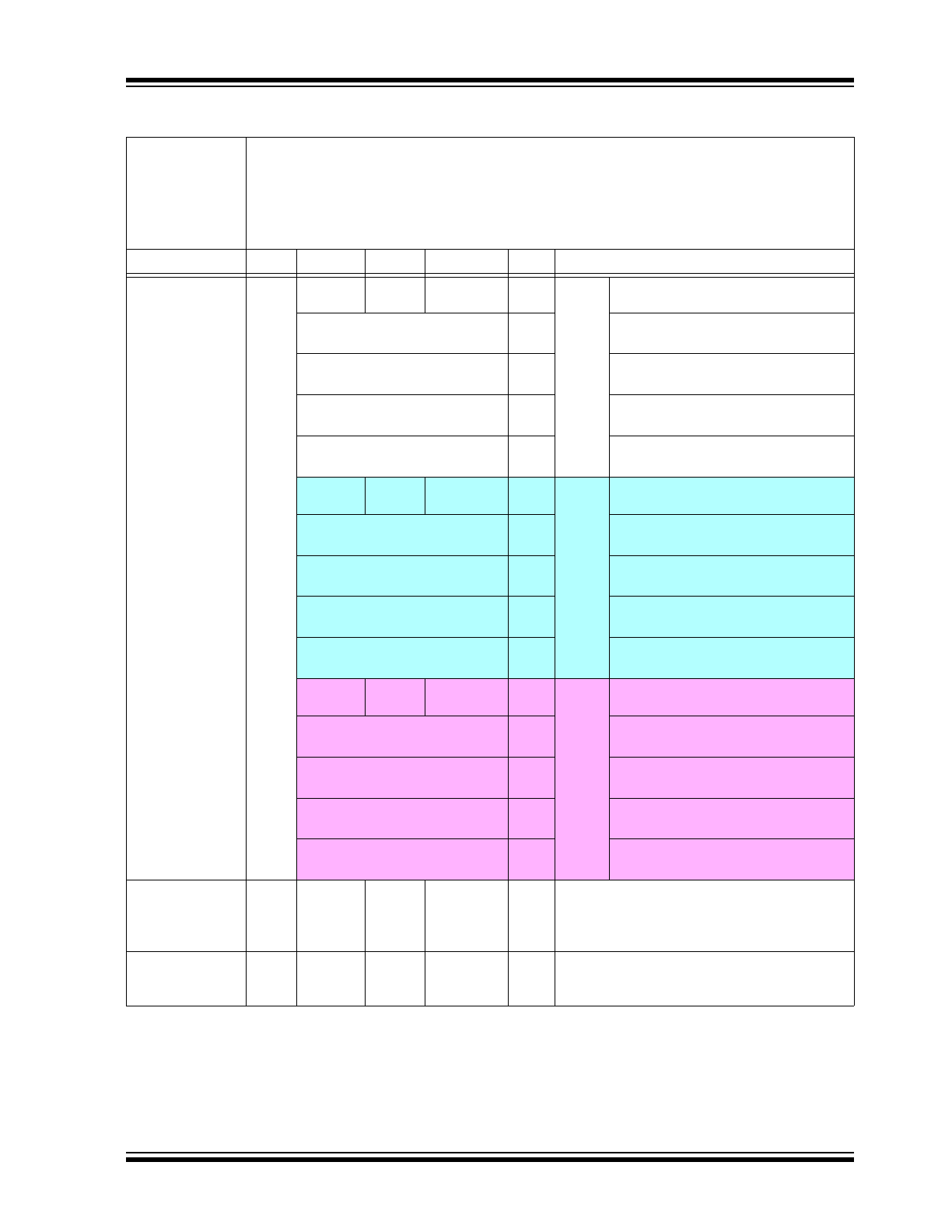
DC CHARACTERISTICS (CONTINUED)
DC
Characteristics
Standard Operating Conditions (unless otherwise specified):
Operating Temperature: -40°C
T
A
+125°C (Extended)
Unless otherwise noted, all parameters apply across these specified operating ranges:
V
DD
= +2.7V to 5.5V, V
REF
= +2.048V to V
DD
, V
SS
= 0V
Gx = ‘0’, R
L
= 5 k
from V
OUT
to V
SS
, C
L
= 100 pF
Typical specifications represent values for V
DD
= 5.5V, T
A
= +25°C.
Parameters
Sym.
Min.
Typ.
Max.
Units
Conditions
Supply Current
I
DD
—
—
320
µA
Single 1MHz
(
2
)
Serial Interface Active
(Not High-Voltage Command)
VRxB:VRxA = ‘01’
(
6
)
V
OUT
is unloaded, V
DD
= 5.5V
Volatile DAC Register = 000h
—
—
910
µA
10 MHz
(
2
)
—
—
1.7
mA
20 MHz
—
—
510
µA
Dual
1 MHz
(
2
)
—
—
1.1
mA
10 MHz
(
2
)
—
—
1.85
mA
20 MHz
—
—
250
µA
Single 1 MHz
(
2
)
Serial Interface Active
(Not High-Voltage Command)
VRxB:VRxA = ‘10’
(
4
)
V
OUT
is unloaded.
V
REF
= V
DD
= 5.5V
Volatile DAC Register = 000h
—
—
840
µA
10 MHz
(
2
)
—
—
1.65
mA
20 MHz
(
2
)
—
—
380
µA
Dual
1 MHz
(
2
)
—
—
970
µA
10 MHz
(
2
)
—
—
1.75
mA
20 MHz
(
2
)
—
—
180
µA
Single Serial Interface Inactive
(
2
)
(Not High-Voltage Command)
VRxB:VRxA = ‘00’
SCK = SDI = V
SS
V
OUT
is unloaded.
Volatile DAC Register = 000h
—
—
380
µA
Dual
—
—
180
µA
Single Serial Interface Inactive
(
2
)
(Not High-Voltage Command)
VRxB:VRxA = ‘11’, V
REF
= V
DD
SCK = SDI = V
SS
V
OUT
is unloaded.
Volatile DAC Register = 000h
—
—
380
µA
Dual
—
145
180
µA
Single HVC = 12.5V (High-Voltage Command)
Serial Interface Inactive
V
REF
= V
DD
= 5.5V, LAT/HVC = V
IHH
DAC registers = 000h
V
OUT
pins are unloaded
—
260
400
µA
Dual
Power-Down
Current
I
DDP
—
0.65
3.8
µA
PDxB:PDxA = ‘01’
(
5
)
V
OUT
not connected
Note 2
This parameter is ensured by characterization.
Note 4
Supply current is independent of current through the resistor ladder in mode VRxB:VRxA = ‘10’.
Note 5
The PDxB:PDxA = ‘01’, ‘10’, and ‘11’ configurations should have the same current.
Note 6
By design, this is the worst-case current mode.
MCP48FVBXX
DS20005466A-page 8
2015 Microchip Technology Inc.
DC CHARACTERISTICS (CONTINUED)
DC Characteristics
Standard Operating Conditions (unless otherwise specified):
Operating Temperature: -40°C
T
A
+125°C (Extended)
Unless otherwise noted, all parameters apply across these specified operating ranges:
V
DD
= +2.7V to 5.5V, V
REF
= +2.048V to V
DD
, V
SS
= 0V
Gx = ‘0’, R
L
= 5 k
from V
OUT
to V
SS
, C
L
= 100 pF
Typical specifications represent values for V
DD
= 5.5V, T
A
= +25°C.
Parameters
Sym.
Min.
Typ.
Max.
Units
Conditions
Resistor Ladder
Resistance
R
L
100
140
180
k
1.8V
V
DD
5.5V
V
REF
1.0V
(
7
)
Resolution
(# of Resistors and
# of Taps)
(see
B.1 “Resolution”
)
N
256
Taps
8-bit
No Missing Codes
1024
Taps
10-bit No Missing Codes
4096
Taps
12-bit No Missing Codes
Nominal V
OUT
Match
(
11
)
|V
OUT
- V
OUTMEAN
|
/V
OUTMEAN
—
0.5
1.0
%
2.7V
V
DD
5.5V
(
2
)
—
—
1.2
%
1.8V
(
2
)
V
OUT
Tempco
(See
B.19 “V
OUT
Tem-
perature Coefficient”
V
OUT
/
T
—
15
—
ppm/°C Code = Mid-scale
(7Fh, 1FFh or 7FFh)
V
REF
pin
Input Voltage Range
V
REF
V
SS
—
V
DD
V
1.8V
V
DD
5.5V
(
1
)
Note 1
This parameter is ensured by design.
Note 2
This parameter is ensured by characterization.
Note 7
Resistance is defined as the resistance between the VREF pin (mode VRxB:VRxA = ‘10’) to VSS pin.
For dual-channel devices (MCP48FVBX2), this is the effective resistance of the each resistor ladder.
The resistance measurement is that of the two resistor ladders measured in parallel.
Note 11
Variation of one output voltage to mean output voltage.
2015 Microchip Technology Inc.
DS20005466A-page 9
MCP48FVBXX
DC CHARACTERISTICS (CONTINUED)
DC
Characteristics
Standard Operating Conditions (unless otherwise specified):
Operating Temperature: -40°C
T
A
+125°C (Extended)
Unless otherwise noted, all parameters apply across these specified operating ranges:
V
DD
= +2.7V to 5.5V, V
REF
= +2.048V to V
DD
, V
SS
= 0V
Gx = ‘0’, R
L
= 5 k
from V
OUT
to V
SS
, C
L
= 100 pF
Typical specifications represent values for V
DD
= 5.5V, T
A
= +25°C.
Parameters
Sym.
Min.
Typ.
Max.
Units
Conditions
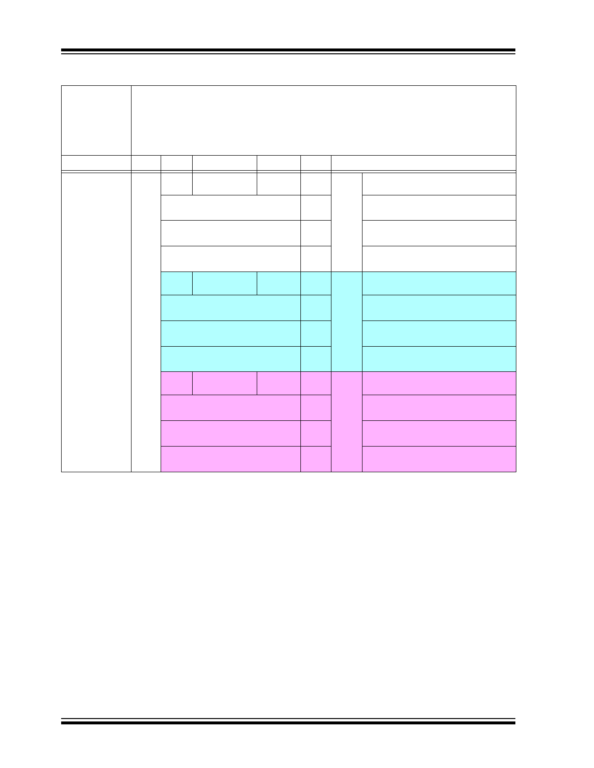
Zero-Scale Error
(see
B.5 “Zero-Scale
Error (E
ZS
)”
)
(Code = 000h)
E
ZS
—
—
0.75
LSb
8-bit
VRxB:VRxA = ‘11’, Gx = ‘0’
V
REF
= V
DD
, No Load
See
Section 2.0, “Typical
Performance Curves”
(
2
)
LSb
VRxB:VRxA = ‘00’, Gx = ‘0’
V
DD
= 5.5V, No Load
See
Section 2.0, “Typical
Performance Curves”
(
2
)
LSb
V
DD
= 1.8V, V
REF
= 1.0V
VRxB:VRxA = ‘10’, Gx = ‘0’, No Load
See
Section 2.0, “Typical
Performance Curves”
(
2
)
LSb
V
DD
= 1.8V, V
REF
= 1.0V
VRxB:VRxA = ‘11’, Gx = ‘0’, No Load
See
Section 2.0, “Typical
Performance Curves”
(
2
)
LSb
VRxB:VRxA = ‘01’, Gx = ‘0’, No Load
—
—
3
LSb
10-bit VRxB:VRxA = ‘11’, Gx = ‘0’
V
REF
= V
DD
, No Load
See
Section 2.0, “Typical
Performance Curves”
(
2
)
LSb
VRxB:VRxA = ‘00’, Gx = ‘0’
V
DD
= 5.5V, No Load
See
Section 2.0, “Typical
Performance Curves”
(
2
)
LSb
V
DD
= 1.8V, V
REF
= 1.0V
VRxB:VRxA = ‘10’, Gx = ‘0’, No Load
See
Section 2.0, “Typical
Performance Curves”
(
2
)
LSb
V
DD
= 1.8V, V
REF
= 1.0V
VRxB:VRxA = ‘11’, Gx = ‘0’, No Load
See
Section 2.0, “Typical
Performance Curves”
(
2
)
LSb
VRxB:VRxA = ‘01’, Gx = ‘0’
No Load
—
—
12
LSb
12-bit VRxB:VRxA = ‘11’, Gx = ‘0’
V
REF
= V
DD
, No Load
See
Section 2.0, “Typical
Performance Curves”
(
2
)
LSb
VRxB:VRxA = ‘00’, Gx = ‘0’
V
DD
= 5.5V, No Load
See
Section 2.0, “Typical
Performance Curves”
(
2
)
LSb
V
DD
= 1.8V, V
REF
= 1.0V
VRxB:VRxA = ‘10’, Gx = ‘0’, No Load
See
Section 2.0, “Typical
Performance Curves”
(
2
)
LSb
V
DD
= 1.8V, V
REF
= 1.0V
VRxB:VRxA = ‘11’, Gx = ‘0’, No Load
See
Section 2.0, “Typical
Performance Curves”
(
2
)
LSb
VRxB:VRxA = ‘01’, Gx = ‘0’
No Load
Offset Error
(see
B.8 “Offset
Error Drift
(E
OSD
)”
)
E
OSD
-15
±1.5
+15
mV
VRxB:VRxA
=
‘00’
Gx = ‘0’
No Load
Offset Voltage
Temperature
Coefficient
V
OSTC
—
±10
—
µV/°C
Note 2
This parameter is ensured by characterization.
MCP48FVBXX
DS20005466A-page 10
2015 Microchip Technology Inc.
DC CHARACTERISTICS (CONTINUED)
DC
Characteristics
Standard Operating Conditions (unless otherwise specified):
Operating Temperature: -40°C
T
A
+125°C (Extended)
Unless otherwise noted, all parameters apply across these specified operating ranges:
V
DD
= +2.7V to 5.5V, V
REF
= +2.048V to V
DD
, V
SS
= 0V
Gx = ‘0’, R
L
= 5 k
from V
OUT
to GND, C
L
= 100 pF
Typical specifications represent values for V
DD
= 5.5V, T
A
= +25°C.
Parameters
Sym.
Min.
Typ.
Max.
Units
Conditions
Full-Scale Error
(see
B.4 “Full-Scale
Error (E
FS
)”
)
E
FS
—
—
4.5
LSb
8-bit
Code = FFh, VRxB:VRxA = ‘11’
Gx = ‘0’, V
REF
= 2.048V, No Load
See
Section 2.0, “Typical
Performance Curves”
(
2
)
LSb
Code = FFh, VRxB:VRxA = ‘10’
Gx = ‘0’, V
REF
= 2.048V, No Load
See
Section 2.0, “Typical
Performance Curves”
(
2
)
LSb
Code = FFh, VRxB:VRxA = ‘01’
Gx = ‘0’, V
REF
= 2.048V, No Load
See
Section 2.0, “Typical
Performance Curves”
(
2
)
LSb
Code = FFh, VRxB:VRxA = ‘00’
No Load
—
—
18
LSb
10-bit Code = 3FFh, VRxB:VRxA = ‘11’
Gx = ‘0’, V
REF
= 2.048V, No Load
See
Section 2.0, “Typical
Performance Curves”
(
2
)
LSb
Code = 3FFh, VRxB:VRxA = ‘10’
Gx = ‘0’, V
REF
= 2.048V, No Load
See
Section 2.0, “Typical
Performance Curves”
(
2
)
LSb
Code = 3FFh, VRxB:VRxA = ‘01’
Gx = ‘0’, V
REF
= 2.048V, No Load
See
Section 2.0, “Typical
Performance Curves”
(
2
)
LSb
Code = 3FFh, VRxB:VRxA = ‘00’
No Load
—
—
70
LSb
12-bit Code = FFFh, VRxB:VRxA = ‘11’
Gx = ‘0’, V
REF
= 2.048V, No Load
See
Section 2.0, “Typical
Performance Curves”
(
2
)
LSb
Code = FFFh, VRxB:VRxA = ‘10’
Gx = ‘0’, V
REF
= 2.048V, No Load
See
Section 2.0, “Typical
Performance Curves”
(
2
)
LSb
Code = FFFh, VRxB:VRxA = ‘01’
Gx = ‘0’, V
REF
= 2.048V, No Load
See
Section 2.0, “Typical
Performance Curves”
(
2
)
LSb
Code = FFFh, VRxB:VRxA = ‘00’
No Load
Note 2
This parameter is ensured by characterization.