
2010-2015 Microchip Technology Inc.
DS20002249B-page 1
MCP4802/4812/4822
Features
• MCP4802: Dual 8-Bit Voltage Output DAC
• MCP4812: Dual 10-Bit Voltage Output DAC
• MCP4822: Dual 12-Bit Voltage Output DAC
• Rail-to-Rail Output
• SPI Interface with 20 MHz Clock Support
• Simultaneous Latching of the Dual DACs
with LDAC pin
• Fast Settling Time of 4.5 µs
• Selectable Unity or 2x Gain Output
• 2.048V Internal Voltage Reference
• 50 ppm/°C V
REF
Temperature Coefficient
• 2.7V to 5.5V Single-Supply Operation
• Extended Temperature Range: -40°C to +125°C
Applications
• Set Point or Offset Trimming
• Sensor Calibration
• Precision Selectable Voltage Reference
• Portable Instrumentation (Battery-Powered)
• Calibration of Optical Communication Devices
Description
The MCP4802/4812/4822 devices are dual 8-bit, 10-bit
and 12-bit buffered voltage output Digital-to-Analog
Converters (DACs), respectively. The devices operate
from a single 2.7V to 5.5V supply with SPI compatible
Serial Peripheral Interface.
The devices have a high precision internal voltage
reference (V
REF
= 2.048V). The user can configure the
full-scale range of the device to be 2.048V or 4.096V by
setting the Gain Selection Option bit (gain of 1 of 2).
Each DAC channel can be operated in Active or
Shutdown mode individually by setting the Configuration
register bits. In Shutdown mode, most of the internal
circuits in the shutdown channel are turned off for power
savings and the output amplifier is configured to present
a known high resistance output load (500 k
typical.
The devices include double-buffered registers,
allowing synchronous updates of two DAC outputs
using the LDAC pin. These devices also incorporate a
Power-on Reset (POR) circuit to ensure reliable power-
up.
The devices utilize a resistive string architecture, with
its inherent advantages of low DNL error, low ratio
metric temperature coefficient and fast settling time.
These devices are specified over the extended
temperature range (+125°C).
The devices provide high accuracy and low noise
performance for consumer and industrial applications
where calibration or compensation of signals (such as
temperature, pressure and humidity) are required.
The MCP4802/4812/4822 devices are available in the
PDIP, SOIC and MSOP packages.
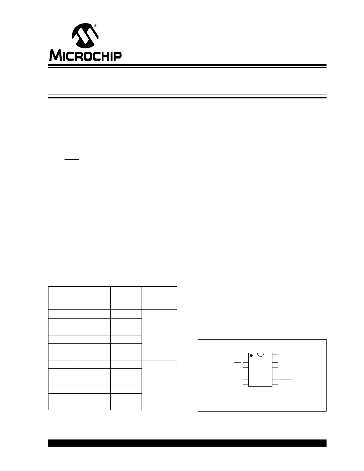
Package Types
Related Products
(1)
P/N
DAC
Resolution
No. of
Channels
Voltage
Reference
(V
REF
)
MCP4801
8
1
Internal
(2.048V)
MCP4811
10
1
MCP4821
12
1
MCP4802
8
2
MCP4812
10
2
MCP4822
12
2
MCP4901
8
1
External
MCP4911
10
1
MCP4921
12
1
MCP4902
8
2
MCP4912
10
2
MCP4922
12
2
Note 1: The products listed here have similar
AC/DC performances.
M
C
P48X2
8-Pin PDIP, SOIC, MSOP
1
2
3
4
8
7
6
5
CS
SCK
SDI
V
DD
V
SS
V
OUTA
V
OUTB
LDAC
MCP4802: 8-bit dual DAC
MCP4812: 10-bit dual DAC
MCP4822: 12-bit dual DAC
8/10/12-Bit Dual Voltage Output Digital-to-Analog Converter
with Internal V
REF
and SPI Interface
MCP4802/4812/4822
DS20002249B-page 2
2010-2015 Microchip Technology Inc.
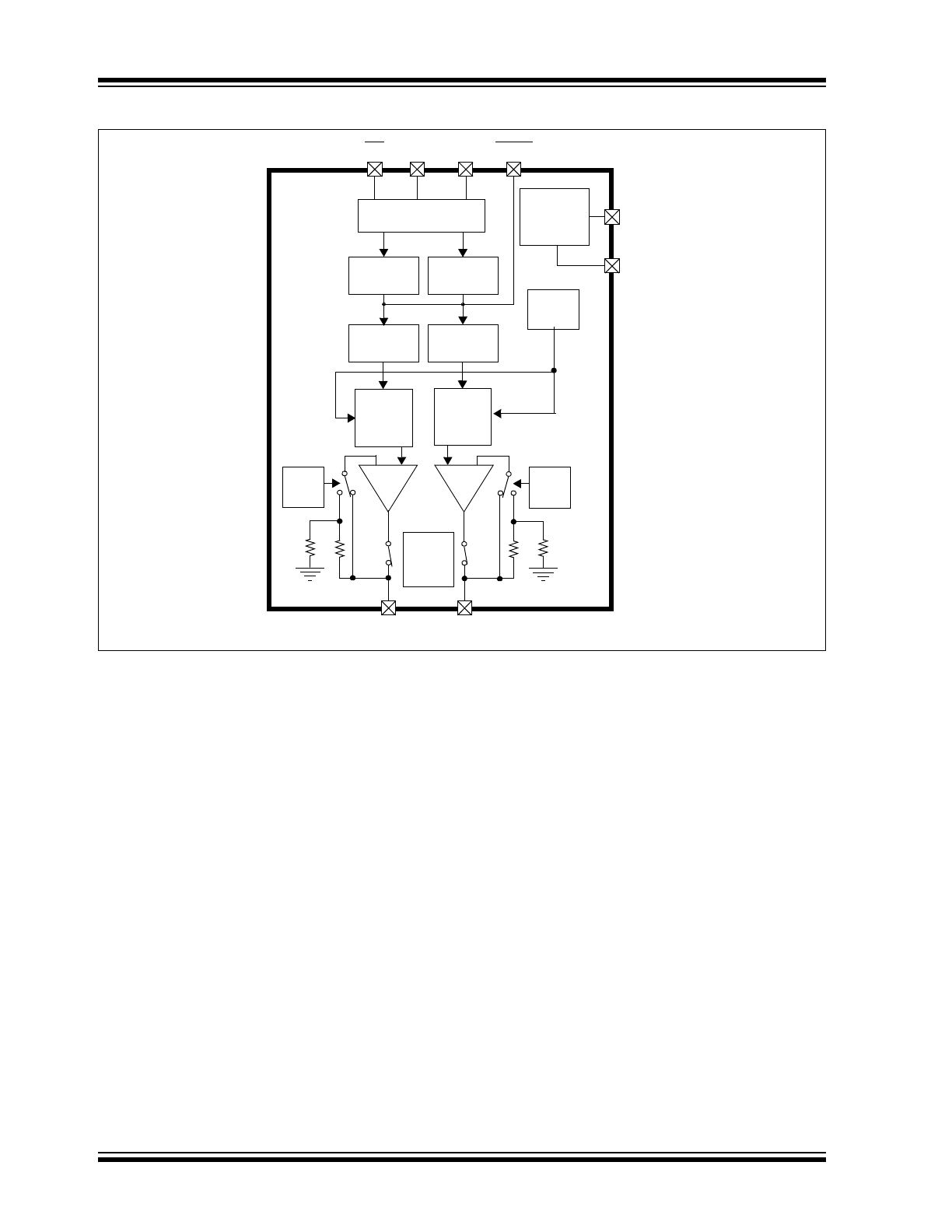
Block Diagram
Op Amps
V
DD
V
SS
CS
SDI
SCK
Interface Logic
Input
Register A Register B
Input
DAC
A
Register
Register
DAC
B
String
DAC
B
String
DAC
A
Output
Power-on
Reset
V
OUTA
V
OUTB
LDAC
Output
Gain
Logic
Gain
Logic
2.048V
V
REF
Logic
2010-2015 Microchip Technology Inc.
DS20002249B-page 3
MCP4802/4812/4822
1.0
ELECTRICAL
CHARACTERISTICS
Absolute Maximum Ratings †
V
DD
....................................................................... 6.5V
All inputs and outputs .......... V
SS
– 0.3V to V
DD
+ 0.3V
Current at Input Pins ......................................... ±2 mA
Current at Supply Pins .................................... ±50 mA
Current at Output Pins .................................... ±25 mA
Storage temperature .......................... -65°C to +150°C
Ambient temp. with power applied ..... -55°C to +125°C
ESD protection on all pins
4 kV (HBM), 400V (MM)
Maximum Junction Temperature (T
J
)................+150°C
† Notice: Stresses above those listed under “Maximum
Ratings” may cause permanent damage to the device.
This is a stress rating only and functional operation of
the device at those or any other conditions above those
indicated in the operational listings of this specification
is not implied. Exposure to maximum rating conditions
for extended periods may affect device reliability.
ELECTRICAL CHARACTERISTICS
Electrical Specifications: Unless otherwise indicated, V
DD
= 5V, V
SS
= 0V, V
REF
= 2.048V,
Output Buffer Gain (G) = 2x, R
L
= 5 k
to GND, C
L
= 100 pF, T
A
= -40 to +85°C. Typical values are at +25°C.
Parameters
Sym
Min
Typ
Max
Units
Conditions
Power Requirements
Input Voltage
V
DD
2.7
—
5.5
V
Input Current
I
DD
—
415
750
µA
All digital inputs are grounded,
all analog outputs (V
OUT
) are
unloaded. Code = 0x000h
Software Shutdown Current
I
SHDN_SW
—
3.3
6
µA
Power-on Reset Threshold
V
POR
—
2.0
—
V
DC Accuracy
MCP4802
Resolution
n
8
—
—
Bits
INL Error
INL
-1
±0.125
1
LSb
DNL
DNL
-0.5
±0.1
+0.5
LSb
Note 1
MCP4812
Resolution
n
10
—
—
Bits
INL Error
INL
-3.5
±0.5
3.5
LSb
DNL DNL
-0.5
±0.1
+0.5
LSb
Note 1
MCP4822
Resolution
n
12
—
—
Bits
INL Error
INL
-12
±2
12
LSb
DNL
DNL
-0.75
±0.2
+0.75
LSb
Note 1
Offset Error
V
OS
-1
±0.02
1
% of FSR Code = 0x000h
Offset Error Temperature
Coefficient
V
OS
/°C
—
0.16
—
ppm/°C
-45°C to +25°C
—
-0.44
—
ppm/°C
+25°C to +85°C
Gain Error
g
E
-2
-0.10
2
% of FSR Code = 0xFFFh,
not including offset error
Gain Error Temperature
Coefficient
G/°C
—
-3
—
ppm/°C
Note 1:
Guaranteed monotonic by design over all codes.
2:
This parameter is ensured by design, and not 100% tested.
MCP4802/4812/4822
DS20002249B-page 4
2010-2015 Microchip Technology Inc.
Internal Voltage Reference (V
REF
)
Internal Reference Voltage
V
REF
2.008
2.048
2.088
V
V
OUTA
when G = 1x and
Code = 0xFFFh
Temperature Coefficient
(
Note 2
)
V
REF
/°C
—
125
325
ppm/°C
-40°C to 0°C
—
0.25
0.65
LSb/°C
-40°C to 0°C
—
45
160
ppm/°C
0°C to +85°C
—
0.09
0.32
LSb/°C
0°C to +85°C
Output Noise (V
REF
Noise)
E
NREF
(0.1-
10 Hz)
—
290
—
µV
p-p
Code = 0xFFFh, G = 1x
Output Noise Density
e
NREF
(1 kHz)
—
1.2
—
µV/
Hz Code = 0xFFFh, G = 1x
e
NREF
(10 kHz)
—
1.0
—
µV/
Hz Code = 0xFFFh, G = 1x
1/f Corner Frequency
f
CORNER
—
400
—
Hz
Output Amplifier
Output Swing
V
OUT
—
0.01 to
V
DD
– 0.04
—
V
Accuracy is better than 1 LSb for
V
OUT
= 10 mV to (V
DD
–40 mV)
Phase Margin
PM
—
66
—
Degree
(°)
C
L
= 400 pF, R
L
=
Slew Rate
SR
—
0.55
—
V/µs
Short Circuit Current
I
SC
—
15
24
mA
Settling Time
t
SETTLING
—
4.5
—
µs
Within 1/2 LSb of final value from
1/4 to 3/4 full-scale range
Dynamic Performance (
Note 2
)
DAC-to-DAC Crosstalk
—
<10
—
nV-s
Major Code Transition Glitch
—
45
—
nV-s
1 LSb change around major carry
(0111...1111 to
1000...0000
)
Digital Feedthrough
—
<10
—
nV-s
Analog Crosstalk
—
<10
—
nV-s
ELECTRICAL CHARACTERISTICS (CONTINUED)
Electrical Specifications: Unless otherwise indicated, V
DD
= 5V, V
SS
= 0V, V
REF
= 2.048V,
Output Buffer Gain (G) = 2x, R
L
= 5 k
to GND, C
L
= 100 pF, T
A
= -40 to +85°C. Typical values are at +25°C.
Parameters
Sym
Min
Typ
Max
Units
Conditions
Note 1:
Guaranteed monotonic by design over all codes.
2:
This parameter is ensured by design, and not 100% tested.
2010-2015 Microchip Technology Inc.
DS20002249B-page 5
MCP4802/4812/4822
ELECTRICAL CHARACTERISTIC WITH EXTENDED TEMPERATURE
Electrical Specifications: Unless otherwise indicated, V
DD
= 5V, V
SS
= 0V, V
REF
= 2.048V, Output Buffer Gain (G) = 2x,
R
L
= 5 k
to GND, C
L
= 100 pF. Typical values are at +125°C by characterization or simulation.
Parameters
Sym
Min
Typ
Max
Units
Conditions
Power Requirements
Input Voltage
V
DD
2.7
—
5.5
V
Input Current
Input Curren
I
DD
—
440
—
µA
All digital inputs are grounded,
all analog outputs (V
OUT
) are
unloaded. Code = 0x000h.
Software Shutdown Current
I
SHDN_SW
—
5
—
µA
Power-On Reset threshold
V
POR
—
1.85
—
V
DC Accuracy
MCP4802
Resolution
n
8
—
—
Bits
INL Error
INL
—
±0.25
—
LSb
DNL
DNL
—
±0.2
—
LSb
Note 1
MCP4812
Resolution
n
10
—
—
Bits
INL Error
INL
—
±1
—
LSb
DNL DNL
—
±0.2
—
LSb
Note 1
MCP4822
Resolution
n
12
—
—
Bits
INL Error
INL
—
±4
—
LSb
DNL
DNL
—
±0.25
—
LSb
Note 1
Offset Error
V
OS
—
±0.02
—
% of FSR
Code = 0x000h
Offset Error Temperature
Coefficient
V
OS
/°C
—
-5
—
ppm/°C
+25°C to +125°C
Gain Error
g
E
—
-0.10
—
% of FSR
Code = 0xFFFh,
not including offset error
Gain Error Temperature
Coefficient
G/°C
—
-3
—
ppm/°C
Internal Voltage Reference (V
REF
)
Internal Reference Voltage
V
REF
—
2.048
—
V
V
OUTA
when G = 1x and
Code = 0xFFFh
Temperature Coefficient
(
Note 2
)
V
REF
/°C
—
125
—
ppm/°C
-40°C to 0°C
—
0.25
—
LSb/°C
-40°C to 0°C
—
45
—
ppm/°C
0°C to +85°C
—
0.09
—
LSb/°C
0°C to +85°C
Output Noise (V
REF
Noise)
E
NREF
(0.1 – 10 Hz)
—
290
—
µV
p-p
Code = 0xFFFh, G = 1x
Output Noise Density
e
NREF
(1 kHz)
—
1.2
—
µV/
Hz
Code = 0xFFFh, G = 1x
e
NREF
(10 kHz)
—
1.0
—
µV/
Hz
Code = 0xFFFh, G = 1x
1/f Corner Frequency
f
CORNER
—
400
—
Hz
Note 1:
Guaranteed monotonic by design over all codes.
2:
This parameter is ensured by design, and not 100% tested.
MCP4802/4812/4822
DS20002249B-page 6
2010-2015 Microchip Technology Inc.
Output Amplifier
Output Swing
V
OUT
—
0.01 to
V
DD
– 0.04
—
V
Accuracy is better than 1 LSb
for
V
OUT
= 10 mV to (V
DD
–
40 mV)
Phase Margin
PM
—
66
—
Degree (°)
C
L
= 400 pF, R
L
=
Slew Rate
SR
—
0.55
—
V/µs
Short Circuit Current
I
SC
—
17
—
mA
Settling Time
t
SETTLING
—
4.5
—
µs
Within 1/2 LSb of final value
from 1/4 to 3/4 full-scale range
Dynamic Performance (
Note 2
)
DAC-to-DAC Crosstalk
—
<10
—
nV-s
Major Code Transition
Glitch
—
45
—
nV-s
1 LSb change around major
carry (0111...1111 to
1000...0000
)
Digital Feedthrough
—
<10
—
nV-s
Analog Crosstalk
—
<10
—
nV-s
AC CHARACTERISTICS (SPI TIMING SPECIFICATIONS)
Electrical Specifications: Unless otherwise indicated, V
DD
= 2.7V – 5.5V, T
A
= -40 to +125°C.
Typical values are at +25°C.
Parameters
Sym
Min
Typ
Max
Units
Conditions
Schmitt Trigger High-Level
Input Voltage
(All digital input pins)
V
IH
0.7 V
DD
—
—
V
Schmitt Trigger Low-Level
Input Voltage
(All digital input pins)
V
IL
—
—
0.2 V
DD
V
Hysteresis of Schmitt Trigger
Inputs
V
HYS
—
0.05 V
DD
—
V
Input Leakage Current
I
LEAKAGE
-1
—
1
A
LDAC = CS = SDI = SCK =
V
DD
or V
SS
Digital Pin Capacitance
(All inputs/outputs)
C
IN
,
C
OUT
—
10
—
pF
V
DD
= 5.0V, T
A
= +25°C,
f
CLK
= 1 MHz (
Note 1
)
Clock Frequency
F
CLK
—
—
20
MHz
T
A
= +25°C (
Note 1
)
Clock High Time
t
HI
15
—
—
ns
Note 1
Clock Low Time
t
LO
15
—
—
ns
Note 1
CS Fall to First Rising CLK
Edge
t
CSSR
40
—
—
ns
Applies only when CS falls with
CLK high. (
Note 1
)
Data Input Setup Time
t
SU
15
—
—
ns
Note 1
Data Input Hold Time
t
HD
10
—
—
ns
Note 1
SCK Rise to CS Rise Hold
Time
t
CHS
15
—
—
ns
Note 1
Note 1:
This parameter is ensured by design and not 100% tested.
ELECTRICAL CHARACTERISTIC WITH EXTENDED TEMPERATURE (CONTINUED)
Electrical Specifications: Unless otherwise indicated, V
DD
= 5V, V
SS
= 0V, V
REF
= 2.048V, Output Buffer Gain (G) = 2x,
R
L
= 5 k
to GND, C
L
= 100 pF. Typical values are at +125°C by characterization or simulation.
Parameters
Sym
Min
Typ
Max
Units
Conditions
Note 1:
Guaranteed monotonic by design over all codes.
2:
This parameter is ensured by design, and not 100% tested.
2010-2015 Microchip Technology Inc.
DS20002249B-page 7
MCP4802/4812/4822
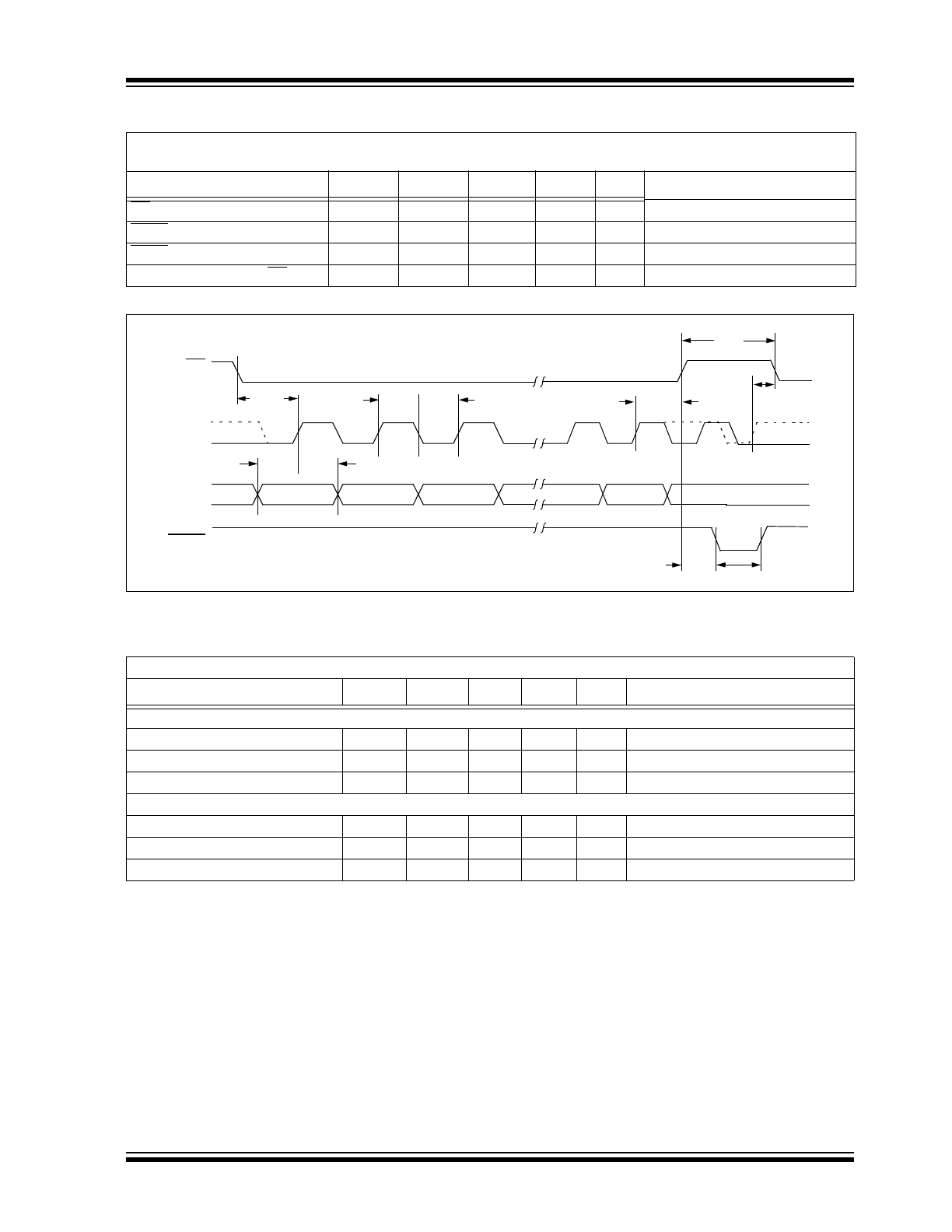
FIGURE 1-1:
SPI Input Timing Data.
TEMPERATURE CHARACTERISTICS
CS High Time
t
CSH
15
—
—
ns
Note 1
LDAC Pulse Width
t
LD
100
—
—
ns
Note 1
LDAC Setup Time
t
LS
40
—
—
ns
Note 1
SCK Idle Time before CS Fall
t
IDLE
40
—
—
ns
Note 1
Electrical Specifications: Unless otherwise indicated, V
DD
= +2.7V to +5.5V, V
SS
= GND.
Parameters
Sym
Min
Typ
Max
Units
Conditions
Temperature Ranges
Specified Temperature Range
T
A
-40
—
+125
°C
Operating Temperature Range
T
A
-40
—
+125
°C
Note 1
Storage Temperature Range
T
A
-65
—
+150
°C
Thermal Package Resistances
Thermal Resistance, 8L-MSOP
JA
—
211
—
°C/W
Thermal Resistance, 8L-PDIP
JA
—
90
—
°C/W
Thermal Resistance, 8L-SOIC
JA
—
150
—
°C/W
Note 1:
The MCP4802/4812/4822 devices operate over this extended temperature range, but with reduced
performance. Operation in this range must not cause T
J
to exceed the maximum junction temperature
of +150°C.
AC CHARACTERISTICS (SPI TIMING SPECIFICATIONS)
Electrical Specifications: Unless otherwise indicated, V
DD
= 2.7V – 5.5V, T
A
= -40 to +125°C.
Typical values are at +25°C.
Parameters
Sym
Min
Typ
Max
Units
Conditions
Note 1:
This parameter is ensured by design and not 100% tested.
CS
SCK
SDI
LDAC
t
CSSR
t
HD
t
SU
t
LO
t
CSH
t
CHS
LSb in
MSb in
t
IDLE
Mode 1,1
Mode 0,0
t
HI
t
LD
t
LS

MCP4802/4812/4822
DS20002249B-page 8
2010-2015 Microchip Technology Inc.
NOTES:
2010-2015 Microchip Technology Inc.
DS20002249B-page 9
MCP4802/4812/4822
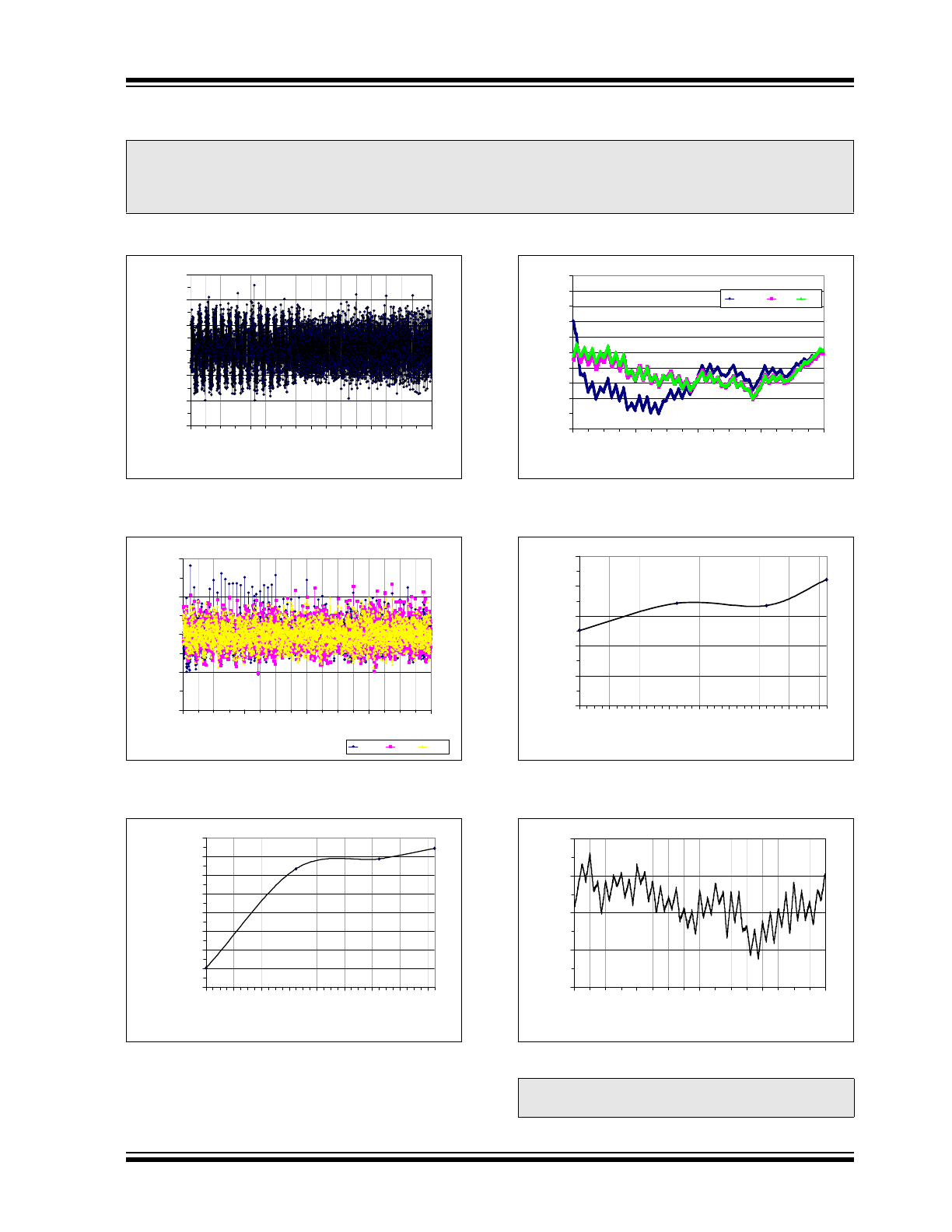
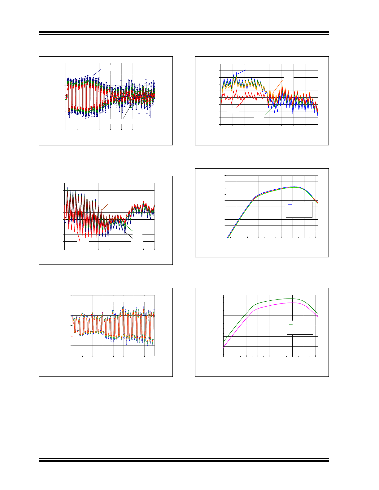
2.0
TYPICAL PERFORMANCE CURVES
Note: Unless otherwise indicated, T
A
= +25°C, V
DD
= 5V, V
SS
= 0V, V
REF
= 2.048V, Gain = 2x, R
L
= 5 k
, C
L
= 100 pF.
FIGURE 2-1:
DNL vs. Code (MCP4822).
FIGURE 2-2:
DNL vs. Code and
Temperature (MCP4822).
FIGURE 2-3:
Absolute DNL vs.
Temperature (MCP4822).
FIGURE 2-4:
INL vs. Code and
Temperature (MCP4822).
FIGURE 2-5:
Absolute INL vs.
Temperature (MCP4822).
FIGURE 2-6:
INL vs. Code (MCP4822).
Note:
The graphs and tables provided following this note are a statistical summary based on a limited number of
samples and are provided for informational purposes only. The performance characteristics listed herein
are not tested or guaranteed. In some graphs or tables, the data presented may be outside the specified
operating range (e.g., outside specified power supply range) and therefore outside the warranted range.
-0.3
-0.2
-0.1
0
0.1
0.2
0.3
0
1024
2048
3072
4096
Code (Decimal)
DN
L
(
L
S
B
)
-0.2
-0.1
0
0.1
0.2
0
1024
2048
3072
4096
Code (Decimal)
DN
L
(
L
S
B
)
125C
85C
25C
0.075
0.0752
0.0754
0.0756
0.0758
0.076
0.0762
0.0764
0.0766
-40
-20
0
20
40
60
80
100 120
Ambient Temperature (ºC)
Ab
s
o
lu
te
DNL
(
L
S
B
)
Note:
Single device graph for illustration of 64
code effect.
-5
-4
-3
-2
-1
0
1
2
3
4
5
0
1024
2048
3072
4096
Code (Decimal)
IN
L (
L
S
B
)
125C
85
25
Ambient Temperature
0
0.5
1
1.5
2
2.5
-40
-20
0
20
40
60
80
100
120
Ambient Temperature (ºC)
Ab
s
o
lu
te
I
N
L
(L
S
B
)
-6
-4
-2
0
2
0
1024
2048
3072
4096
Code (Decimal)
IN
L (
L
SB
)
MCP4802/4812/4822
DS20002249B-page 10
2010-2015 Microchip Technology Inc.
Note: Unless otherwise indicated, T
A
= +25°C, V
DD
= 5V, V
SS
= 0V, V
REF
= 2.048V, Gain = 2x, R
L
= 5 k
, C
L
= 100 pF.
FIGURE 2-7:
DNL vs. Code and
Temperature (MCP4812).
FIGURE 2-8:
INL vs. Code and
Temperature (MCP4812).
FIGURE 2-9:
DNL vs. Code and
Temperature (MCP4802).
FIGURE 2-10:
INL vs. Code and
Temperature (MCP4802).
FIGURE 2-11:
Full-Scale V
OUTA
vs.
Ambient Temperature and V
DD
. Gain = 1x.
FIGURE 2-12:
Full-Scale V
OUTA
vs.
Ambient Temperature and V
DD
. Gain = 2x.
-0.3
-0.2
-0.1
0
0.1
0.2
0.3
0
128
256
384
512
640
768
896 1024
Code
DNL
(
L
S
B
)
- 40
o
C
+25
o
C to +125
o
C
-3
-2.5
-2
-1.5
-1
-0.5
0
0.5
1
1.5
0
128
256
384
512
640
768
896 1024
Code
IN
L
(
L
S
B
)
25
o
C
85
o
C
125
o
C
- 40
o
C
-0.15
-0.1
-0.05
0
0.05
0.1
0.15
0
32
64
96
128 160 192 224 256
Code
DNL
(
L
S
B
)
34
Temperature: - 40
o
C to +125
o
C
-0.3
-0.2
-0.1
0
0.1
0.2
0.3
0.4
0.5
0.6
0
32
64
96
128
160
192
224
256
Code
IN
L
(
L
SB
)
- 40
o
C
25
o
C
85
o
C
125
o
C
2.040
2.041
2.042
2.043
2.044
2.045
2.046
2.047
2.048
2.049
2.050
-40
-20
0
20
40
60
80
100 120
Ambient Temperature (°C)
F
u
ll
S
c
a
le
V
OU
T
(V
)
VDD: 4V
VDD: 3V
VDD: 2.7V
4.076
4.080
4.084
4.088
4.092
4.096
4.100
-40
-20
0
20
40
60
80
100
120
Ambient Temperature (°C)
Fu
ll
S
c
a
le
V
OU
T
(V
)
VDD: 5.5V
VDD: 5V