
2012 Microchip Technology Inc.
DS25154A-page 1
MCP47A1
Features:
• 6-Bit DAC
- 65 Taps: 64 Resistors with Taps to Full-Scale
and Zero-Scale (Wiper Code 00h to 40h)
• V
REF
Pull-down Resistance: 20 k
(typical)
• V
OUT
Voltage Range
- V
SS
to V
REF
• I
2
C
™
Protocol
- Supports SMBus 2.0 Write Byte/Word
Protocol Formats
- Supports SMBus 2.0 Read Byte/Word
Protocol Formats
- Slave Addresses: 5Ch and 7Ch
• Brown-out Reset Protection (1.5V typical)
• Power-on Default Wiper Setting (Mid-scale)
• Low-Power Operation: 90 µA Static Current (typical)
• Wide Operating Voltage Range:
- 1.8V to 5.5V
• Low Tempco: 15 ppm (typical)
• 100 kHz (typical) Bandwidth (-3 dB) Operation
• Extended Temperature Range (-40°C to +125°C)
• Small Packages, SC70-6
• Lead Free (Pb-free) Package
Applications
• Set point or offset trimming
• Cost-sensitive mechanical trim pot replacement
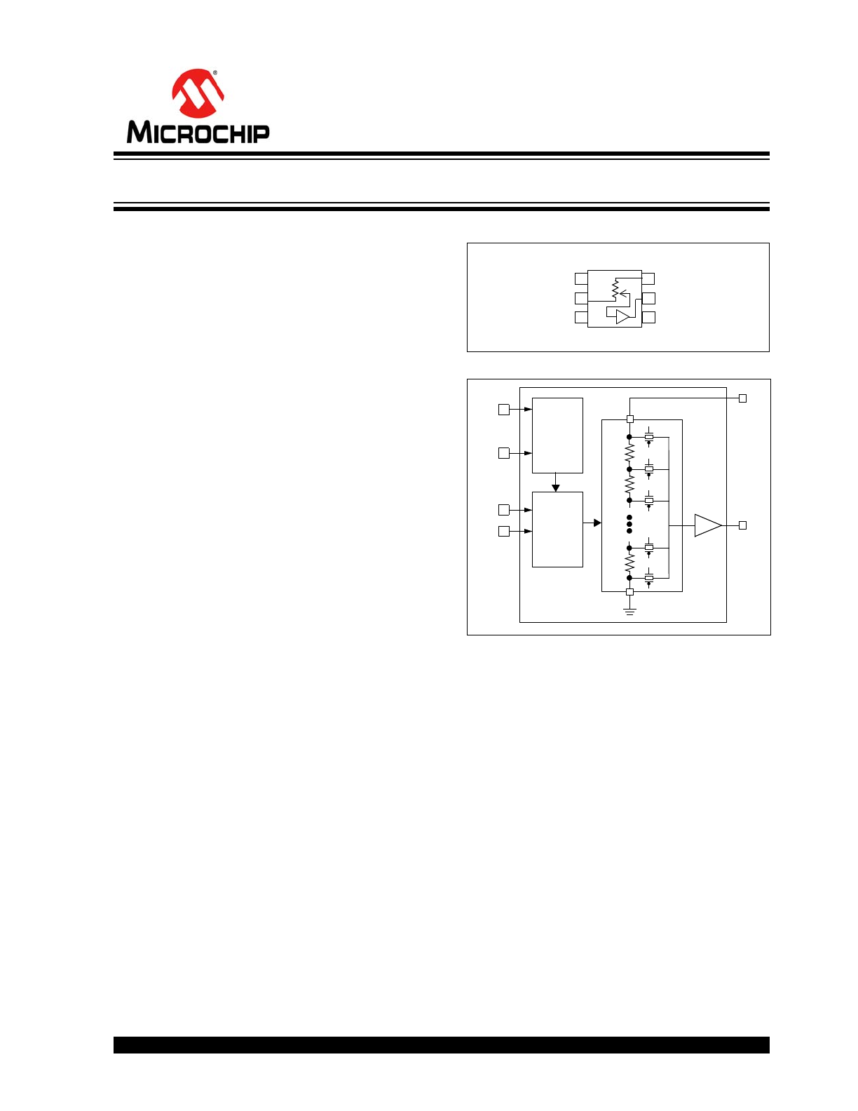
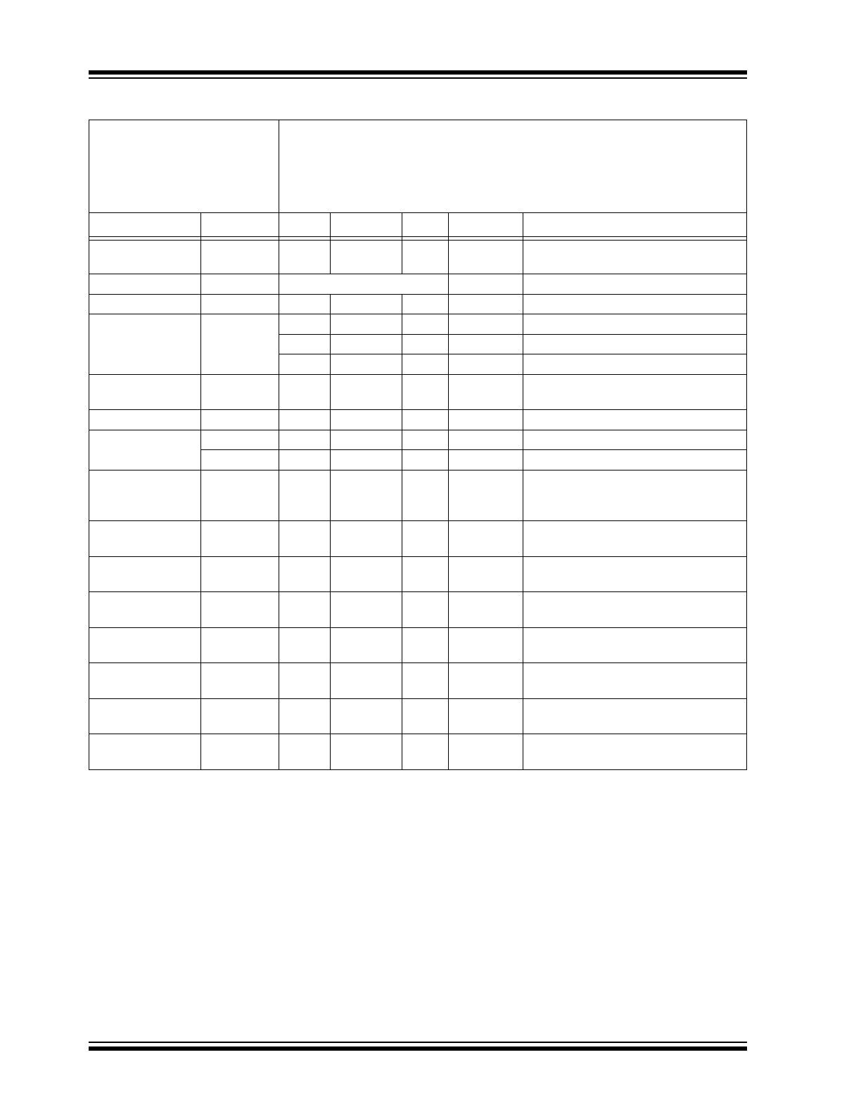
Package Types
Device Block Diagram
Description
The MCP47A1 devices are volatile, 6-Bit digital
potentiometers with a buffered output. The wiper
setting is controlled through an I
2
C serial interface. The
I
2
C slave addresses of “010 1110” and “011 1110”
are supported.
MCP47A1
SC70-6
4
1
2
3
6 V
REF
SDA
V
DD
V
SS
SCL
5 V
OUT
A
W
B
V
DD
V
SS
SCL
V
OUT
B
W
iper
R
e
g
ister
(R
AB
=
2
0
K
)
SDA
V
REF
2-Wire
Interface
and
Control
Logic
Power-up
and
Brown-out
Control
A
6-Bit Volatile DAC with Command Code
MCP47A1
DS25154A-page 2
2012 Microchip Technology Inc.
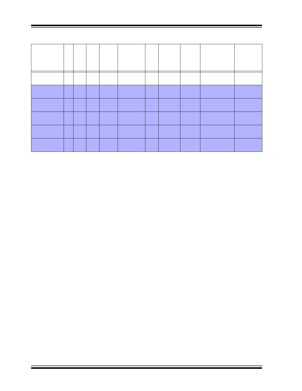
Device Features
Device
In
terfac
e
# o
f T
a
p
s
# o
f
Re
s
is
to
rs
V
RE
F
R
esist
anc
e
(k
)
Da
ta
Va
lu
e
Ra
nge
POR/BOR
Va
lu
e
I
2
C
S
lav
e
Add
re
s
s
V
DD
Op
er
at
in
g
Ra
nge
V
OU
T
Ra
nge
Package(s)
MCP47A1 I
2
C
65
64
20
00h - 40h
20h
5Ch, 7Ch 1.8V
(
1
)
to 5.5V
V
SS
to V
REF
SC70-6
MCP47DA1
(
2
)
I
2
C
65
64
30
00h - 7Fh
40h
5Ch, 7Ch 1.8V
(
1
)
to 5.5V
1/3 V
REF
to
2/3 V
REF
SC70-6,
SOT-23-6
MCP4706
I
2
C
256
256
210
00h - FFh
7Fh
Cxh
(
3
)
2.7V to
5.5V
V
SS
to V
DD
or
V
SS
to V
REF
(
5
)
SOT-23-6,
DFN-6 (2x2)
MCP4716
I
2
C 1024 1024
210
000h - 3FFh 1FFh
Cxh
(
3
)
2.7V to
5.5V
V
SS
to V
DD
or
V
SS
to V
REF
(
5
)
SOT-23-6,
DFN-6 (2x2)
MCP4726
I
2
C 4096 4096
210
000h - FFFh 3FFh
Cxh
(
3
)
2.7V to
5.5V
V
SS
to V
DD
or
V
SS
to V
REF
(
5
)
SOT-23-6,
DFN-6 (2x2)
MCP4725
I
2
C 4096 4096
N.A.
000h - FFFh 3FFh
Cxh
(
4
)
2.7V to
5.5V
V
SS
to V
DD
SOT-23-6
Note 1: Analog characteristics only tested from 2.7V to 5.5V.
2: Refer to MCP47DA1 Data Sheet (DS25118).
3: The A2:A0 bits are determined by device ordered.
4: The A2 and A1 bits are determined by device ordered and A0 is determined by the state of the A0 pin.
5: User programmable.

2012 Microchip Technology Inc.
DS25154A-page 3
MCP47A1
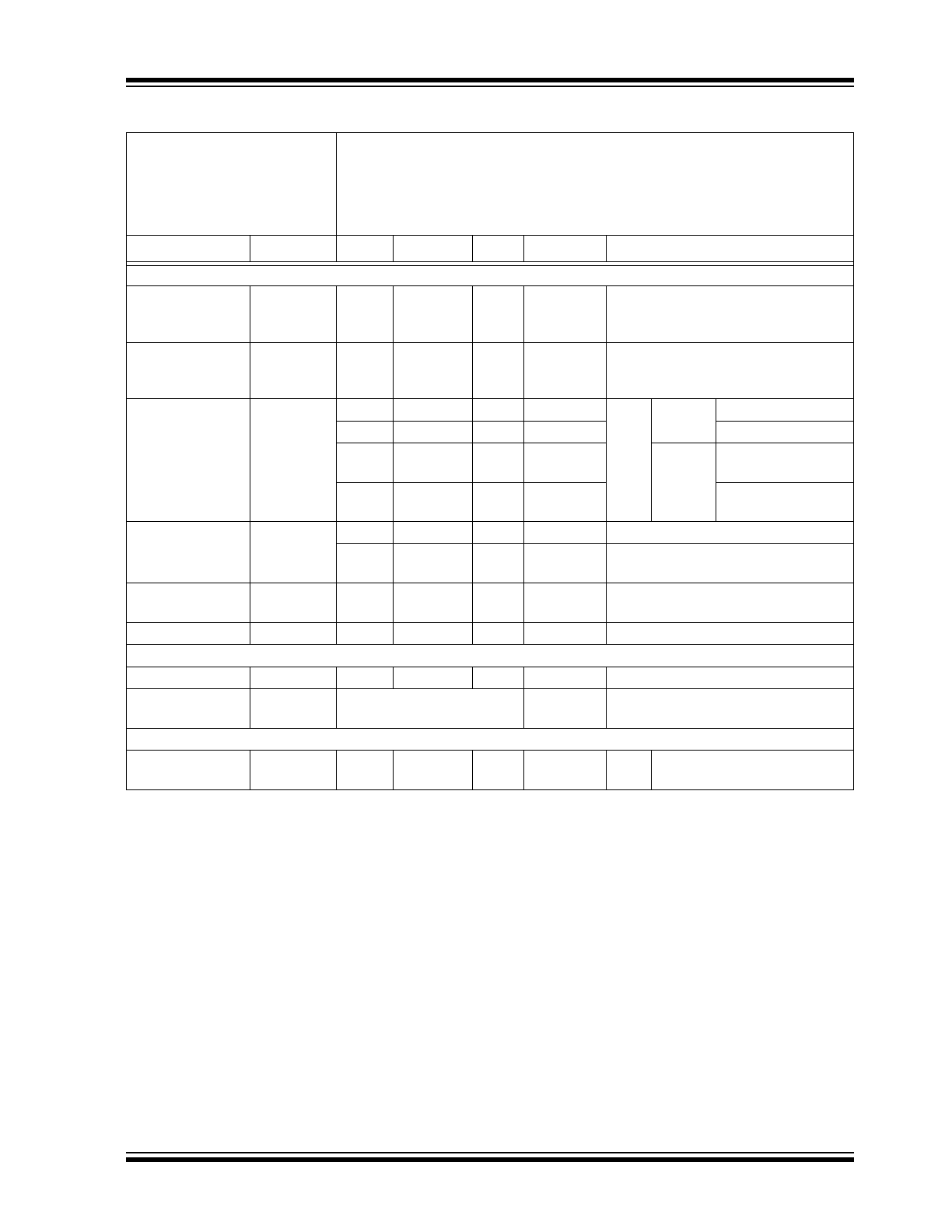
1.0
ELECTRICAL CHARACTERISTICS
Absolute Maximum Ratings †
Voltage on V
DD
with respect to V
SS
.......................................................................................................... 0.6V to +7.0V
Voltage on SCL, and SDA with respect to V
SS
.....................................................................................................
-0.6V to V
DD
+ 0.3V
Voltage on all other pins (V
OUT
and V
REF
) with respect to V
SS
.....................................................................
-0.3V to V
DD
+ 0.3V
Input clamp current, I
IK
(V
I
< 0, V
I
> V
DD
) ............................................................................................................ ±20 mA
Output clamp current, I
OK
(V
O
< 0 or V
O
> V
DD
).................................................................................................. ±20 mA
Maximum output current sunk by any Output pin .................................................................................................. 25 mA
Maximum output current sourced by any Output pin ............................................................................................ 25 mA
Maximum current out of V
SS
pin .......................................................................................................................... 100 mA
Maximum current into V
DD
pin ............................................................................................................................. 100 mA
Maximum current into V
REF
pin............................................................................................................................. 250 uA
Maximum current sourced by V
OUT
pin ................................................................................................................. 40 mA
Maximum current sunk by V
REF
pin ....................................................................................................................... 40 mA
Package power dissipation (T
A
= +50°C, T
J
= +150°C)
SC70-6 ..................................................................................................................................................... 480 mW
Storage temperature .............................................................................................................................. -65°C to +150°C
Ambient temperature with power applied .............................................................................................. -40°C to +125°C
ESD protection on all pins ..........................................................................................................................
6 kV (HBM)
.....................................................................................................................................................................
400V (MM)
1.5 kV (CDM)
Latchup (JEDEC JESD78A) at +125°C ............................................................................................................. ±100 mA
Soldering temperature of leads (10 seconds) ...................................................................................................... +300°C
Maximum Junction Temperature (T
J
) .................................................................................................................. +150°C
† Notice: Stresses above those listed under “Maximum Ratings” may cause permanent damage to the device. This is
a stress rating only and functional operation of the device at those or any other conditions above those indicated in the
operational listings of this specification is not implied. Exposure to maximum rating conditions for extended periods may
affect device reliability.
MCP47A1
DS25154A-page 4
2012 Microchip Technology Inc.
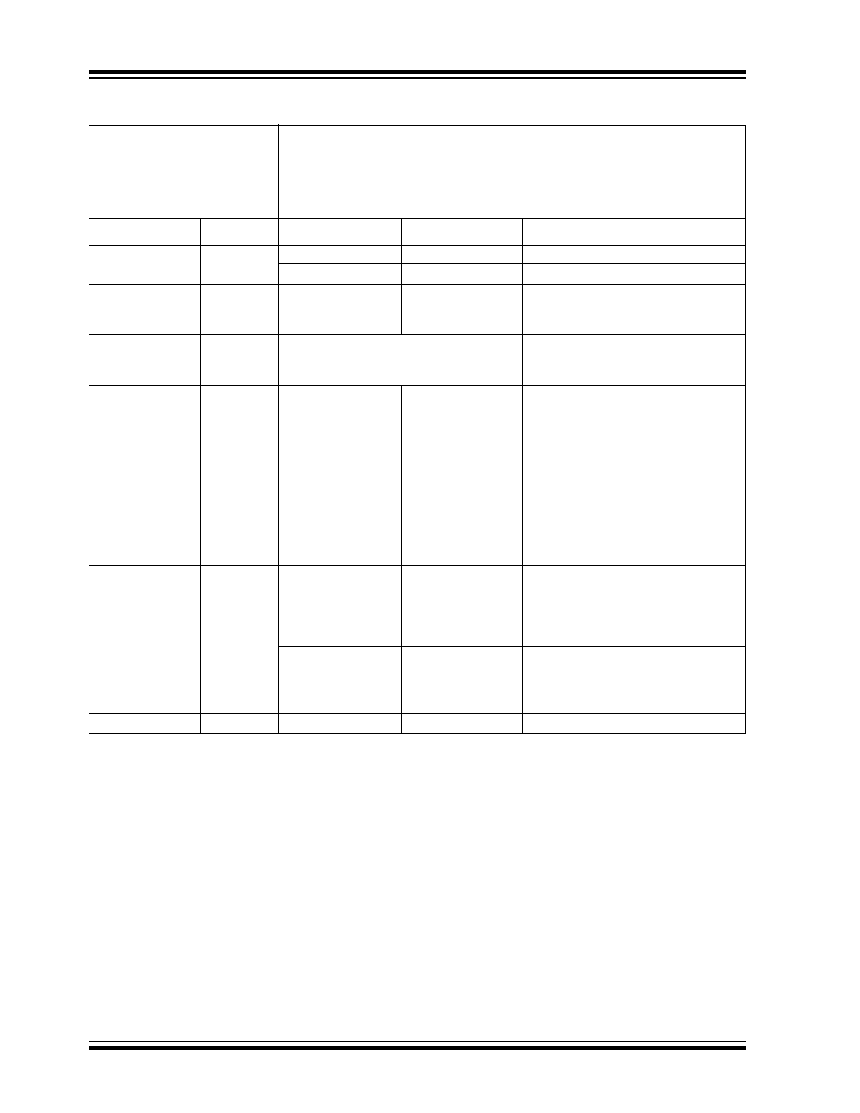
AC/DC CHARACTERISTICS
DC Characteristics
Standard Operating Conditions (unless otherwise specified)
Operating Temperature
–40°C
T
A
+125°C (extended)
All parameters apply across the specified operating ranges unless noted.
V
DD
= +2.7V to +5.5V. C
L
= 1 nF, R
L
= 5 k
.
Typical specifications represent values for V
DD
= 5.5V, T
A
= +25°C.
Parameters
Sym
Min
Typ
Max
Units
Conditions
Supply Voltage
V
DD
2.7
—
5.5
V
Analog Characteristics specified
1.8
—
5.5
V
Digital Characteristics specified
V
DD
Start Voltage
to ensure Wiper to
default reset state
V
BOR
—
—
1.65
V
RAM retention voltage (V
RAM
) < V
BOR
V
DD
Rise Rate to
ensure Power-on
Reset
V
DDRR
Note 5
V/ms
Delay after device
exits the reset
state
(V
DD
> V
BOR
) to
Digital Interface
Active
T
BORD
—
—
1
µS
Delay after device
exits the reset
state
(V
DD
> V
BOR
) to
V
OUT
valid
T
OUTV
20
µS
Within ± 0.5 LSb of V
REF
/ 2
(for default POR/BOR wiper value).
Supply Current
(
Note 6
)
I
DD
—
130
220
µA
Serial Interface Active,
Write all 0’s to Volatile Wiper,
No Load on V
OUT
V
DD
= 5.5V, V
REF
= V
DD
,
F
SCL
= 400 kHz
—
90
130
µA
Serial Interface Inactive (Static),
(Stop condition, SCL = SDA = V
IH
),
No Load on V
OUT
Wiper = 0, V
DD
= 5.5V, V
REF
= V
DD
V
REF
Input Range
V
REF
1
—
V
DD
V
Note 7
Note 1:
Resistance is defined as the resistance between the V
REF
pin and the V
SS
pin.
2:
INL and DNL are measured at V
OUT
from Code = 00h (Zero-Scale) through Code = 3Fh (Full-Scale - 1).
3:
This specification by design.
4:
Nonlinearity is affected by wiper resistance (R
W
), which changes significantly over voltage and
temperature.
5:
POR/BOR is not rate dependent.
6:
Supply current is independent of V
REF
current.
7:
See
Section 7.1.3
.
2012 Microchip Technology Inc.
DS25154A-page 5
MCP47A1
Output Amplifier
Minimum Output
Voltage
V
OUT(MIN)
—
V
SS
—
V
Device Output minimum drive
Maximum Output
Voltage
V
OUT(MAX)
—
V
REF
—
V
Device Output maximum drive
Phase Margin
PM
—
66
—
Degree (°)
C
L
= 400 pF, R
L
=
Slew Rate
SR
—
0.55
—
V/µs
Short Circuit
Current
I
SC
5
15
24
mA
Settling Time
t
SETTLING
—
15
—
µs
External Reference (V
REF
) (
Note 3
)
Input Capacitance
C
VREF
—
7
—
pF
Total Harmonic
Distortion
THD
—
-73
—
dB
V
REF
= 1.65V ± 0.1V,
Frequency = 1 kHz
Dynamic Performance (
Note 3
)
Major Code
Transition Glitch
—
45
—
nV-s
1 LSb change around major carry
(20h to 1Fh)
Digital
Feedthrough
—
<10
—
nV-s
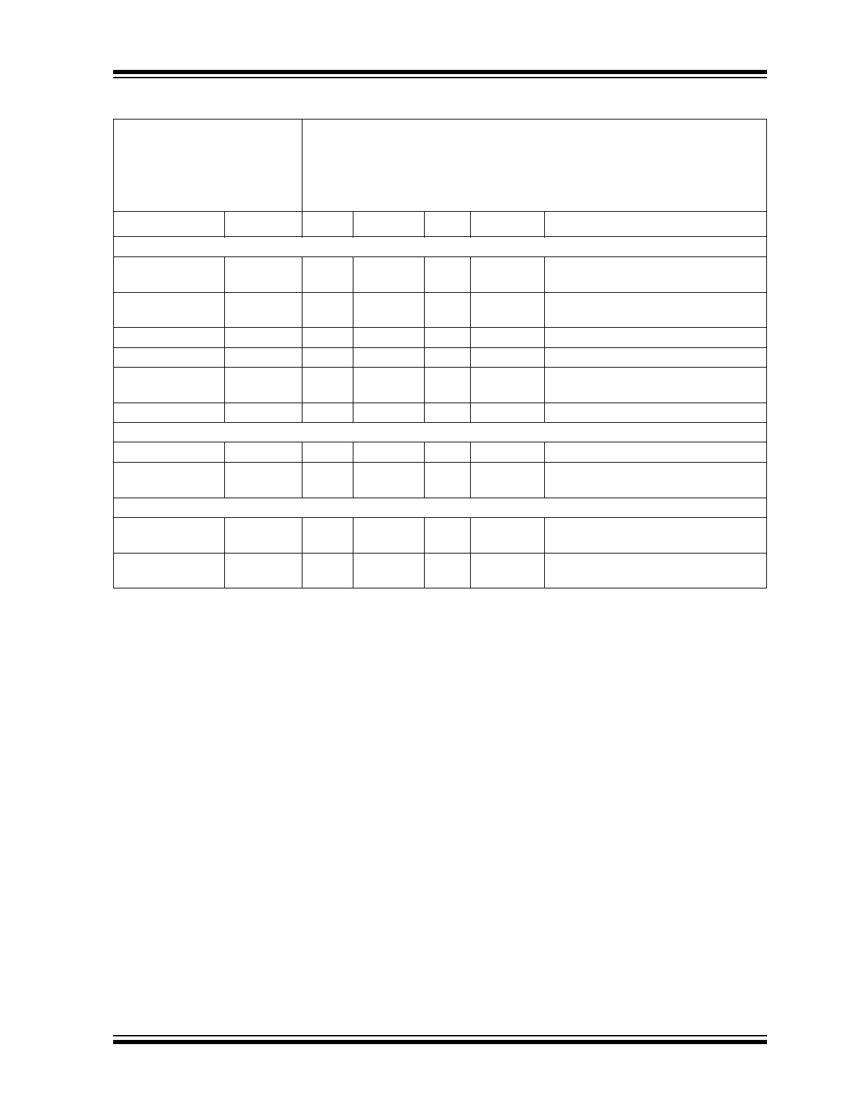
AC/DC CHARACTERISTICS (CONTINUED)
DC Characteristics
Standard Operating Conditions (unless otherwise specified)
Operating Temperature
–40°C
T
A
+125°C (extended)
All parameters apply across the specified operating ranges unless noted.
V
DD
= +2.7V to +5.5V. C
L
= 1 nF, R
L
= 5 k
.
Typical specifications represent values for V
DD
= 5.5V, T
A
= +25°C.
Parameters
Sym
Min
Typ
Max
Units
Conditions
Note 1:
Resistance is defined as the resistance between the V
REF
pin and the V
SS
pin.
2:
INL and DNL are measured at V
OUT
from Code = 00h (Zero-Scale) through Code = 3Fh (Full-Scale - 1).
3:
This specification by design.
4:
Nonlinearity is affected by wiper resistance (R
W
), which changes significantly over voltage and
temperature.
5:
POR/BOR is not rate dependent.
6:
Supply current is independent of V
REF
current.
7:
See
Section 7.1.3
.
MCP47A1
DS25154A-page 6
2012 Microchip Technology Inc.
Resistance
(± 20%)
R
VREF
16.0
20
24.0
k
Note 1
,
Resolution
N
65
Taps
No Missing Codes
Step Resistance
R
S
—
R
VREF
/ 64
—
Note 3
Nominal
Resistance
Tempco
R
VREF
/
T
—
50
—
ppm/°C
T
A
= -20°C to +70°C
—
100
—
ppm/°C
T
A
= -40°C to +85°C
—
150
—
ppm/°C
T
A
= -40°C to +125°C
Ratiometeric
Tempco
V
OUT
/
T
—
15
—
ppm/°C
Code = Midscale (20h)
V
OUT
Accuracy
0.72
0.75
0.78
V
V
REF
= 1.5V, code = 20h
V
OUT
Load
L
VOUTR
5
—
—
k
Resistive
Load
L
VOUTC
—
—
1
nF
Capacitive
Load
Maximum current
through Terminal
(V
REF
)
Note 3
I
VREF
—
—
345
µA
V
REF
= 5.5V
Leakage current
into V
REF
I
L
—
100
—
nA
V
REF
= V
SS
Full-Scale Error
(code = 40h)
V
FSE
-1
±0.35
+1
LSb
V
REF
= V
DD
Zero-Scale Error
(code = 00h)
V
ZSE
-0.75
±0.35
+0.75
LSb
V
REF
= V
DD
V
OUT
Integral
Nonlinearity
INL
-1
±0.25
+1
LSb
Note 2
, V
REF
= V
DD
V
OUT
Differential
Nonlinearity
DNL
-0.5
±0.25
+0.5
LSb
Note 2
, V
REF
= V
DD
Bandwidth -3 dB
BW
—
100
—
kHz
V
DD
= 5.0V, V
REF
= 3.0V ± 2.0V,
Code = 20h
Capacitance
(V
REF
)
C
REF
—
75
—
pF
f =1 MHz, Code = Full-Scale
AC/DC CHARACTERISTICS (CONTINUED)
DC Characteristics
Standard Operating Conditions (unless otherwise specified)
Operating Temperature
–40°C
T
A
+125°C (extended)
All parameters apply across the specified operating ranges unless noted.
V
DD
= +2.7V to +5.5V. C
L
= 1 nF, R
L
= 5 k
.
Typical specifications represent values for V
DD
= 5.5V, T
A
= +25°C.
Parameters
Sym
Min
Typ
Max
Units
Conditions
Note 1:
Resistance is defined as the resistance between the V
REF
pin and the V
SS
pin.
2:
INL and DNL are measured at V
OUT
from Code = 00h (Zero-Scale) through Code = 3Fh (Full-Scale - 1).
3:
This specification by design.
4:
Nonlinearity is affected by wiper resistance (R
W
), which changes significantly over voltage and
temperature.
5:
POR/BOR is not rate dependent.
6:
Supply current is independent of V
REF
current.
7:
See
Section 7.1.3
.
2012 Microchip Technology Inc.
DS25154A-page 7
MCP47A1
Digital Inputs/Outputs (SDA, SCK)
Schmitt Trigger
High Input
Threshold
V
IH
0.7 V
D
D
—
—
V
1.8V
V
DD
5.5V
Schmitt Trigger
Low Input
Threshold
V
IL
-0.5
—
0.3V
D
D
V
1.8V
V
DD
5.5V
Hysteresis of
Schmitt Trigger
Inputs
(
Note 3
)
V
HYS
N.A.
—
—
V
SDA
and
SCL
100 kHz
V
DD
< 2.0V
N.A.
—
—
V
V
DD
2.0V
0.1 V
D
D
—
—
V
400 kHz
V
DD
< 2.0V
0.05 V
DD
—
—
V
V
DD
2.0V
Output Low
Voltage (SDA)
V
OL
V
SS
—
0.4
V
V
DD
2.0V, I
OL
= 3 mA
V
SS
—
0.2V
D
D
V
V
DD
< 2.0V, I
OL
= 1 mA
Input Leakage
Current
I
IL
-1
—
1
µA
V
REF
= V
DD
and V
REF
= V
SS
Pin Capacitance
C
IN
, C
OUT
—
10
—
pF
f
C
= 400 kHz
RAM (Wiper) Value
Value Range
N
0h
—
40h
hex
Wiper POR/BOR
Value
N
POR/BOR
20h
hex
Power Requirements
Power Supply
Sensitivity
PSS
—
0.0015
0.003
5
%/%
V
REF
= V
DD
, Code = 20h
AC/DC CHARACTERISTICS (CONTINUED)
DC Characteristics
Standard Operating Conditions (unless otherwise specified)
Operating Temperature
–40°C
T
A
+125°C (extended)
All parameters apply across the specified operating ranges unless noted.
V
DD
= +2.7V to +5.5V. C
L
= 1 nF, R
L
= 5 k
.
Typical specifications represent values for V
DD
= 5.5V, T
A
= +25°C.
Parameters
Sym
Min
Typ
Max
Units
Conditions
Note 1:
Resistance is defined as the resistance between the V
REF
pin and the V
SS
pin.
2:
INL and DNL are measured at V
OUT
from Code = 00h (Zero-Scale) through Code = 3Fh (Full-Scale - 1).
3:
This specification by design.
4:
Nonlinearity is affected by wiper resistance (R
W
), which changes significantly over voltage and
temperature.
5:
POR/BOR is not rate dependent.
6:
Supply current is independent of V
REF
current.
7:
See
Section 7.1.3
.
MCP47A1
DS25154A-page 8
2012 Microchip Technology Inc.
1.1
I
2
C Mode Timing Waveforms and Requirements
FIGURE 1-1:
I
2
C Bus Start/Stop Bits Timing Waveforms.
FIGURE 1-2:
I
2
C Bus Data Timing.
TABLE 1-1:
I
2
C BUS START/STOP BITS REQUIREMENTS
91
93
SCL
SDA
START
Condition
STOP
Condition
90
92
I
2
C AC Characteristics
Standard Operating Conditions (unless otherwise specified)
Operating Temperature
–40
C T
A
+125C (Extended)
Operating Voltage V
DD
range is described in
Section 2.0 “Typical
Performance Curves”
Param.
No.
Symbol
Characteristic
Min
Max
Units
Conditions
F
SCL
Standard
Mode
0
100
kHz
C
b
= 400 pF, 1.8V - 5.5V
Fast Mode
0
400
kHz
C
b
= 400 pF, 2.7V - 5.5V
D102
Cb
Bus capacitive
loading
100 kHz mode
—
400
pF
400 kHz mode
—
400
pF
90
T
SU
:
STA
START condition
100 kHz mode
4700
—
ns
Only relevant for repeated
START condition
Setup time
400 kHz mode
600
—
ns
91
T
HD
:
STA
START condition
100 kHz mode
4000
—
ns
After this period, the first
clock pulse is generated
Hold time
400 kHz mode
600
—
ns
92
T
SU
:
STO
STOP condition
100 kHz mode
4000
—
ns
Setup time
400 kHz mode
600
—
ns
93
T
HD
:
STO
STOP condition
100 kHz mode
4000
—
ns
Hold time
400 kHz mode
600
—
ns
Note:
Refer to specification D102 (Cb) for load conditions.
90
91
92
100
101
103
106
107
109
109
110
102
SCL
SDA
In
SDA
Out
2012 Microchip Technology Inc.
DS25154A-page 9
MCP47A1
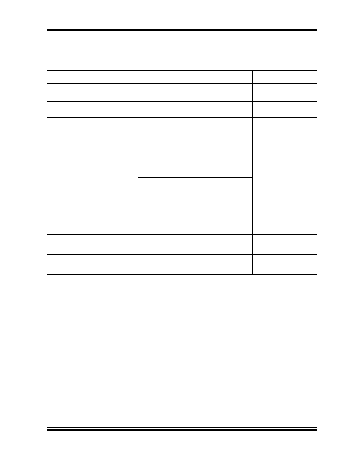
TABLE 1-2:
I
2
C BUS DATA REQUIREMENTS (SLAVE MODE)
I
2
C AC Characteristics
Standard Operating Conditions (unless otherwise specified)
Operating Temperature
–40
C T
A
+125C (Extended)
Operating Voltage V
DD
range is described in
AC/DC characteristics
Parame-
ter No.
Sym
Characteristic
Min
Max
Units
Conditions
100
T
HIGH
Clock high time
100 kHz mode
4000
—
ns
1.8V-5.5V
400 kHz mode
600
—
ns
2.7V-5.5V
101
T
LOW
Clock low time
100 kHz mode
4700
—
ns
1.8V-5.5V
400 kHz mode
1300
—
ns
2.7V-5.5V
102A
(
5
)
T
RSCL
SCL rise time
100 kHz mode
—
1000
ns
C
b
is specified to be from
10 to 400 pF
400 kHz mode
20 + 0.1Cb
300
ns
102B
(
5
)
T
RSDA
SDA rise time
100 kHz mode
—
1000
ns
C
b
is specified to be from
10 to 400 pF
400 kHz mode
20 + 0.1Cb
300
ns
103A
(
5
)
T
FSCL
SCL fall time
100 kHz mode
—
300
ns
C
b
is specified to be from
10 to 400 pF
400 kHz mode
20 + 0.1Cb
40
ns
103B
(
5
)
T
FSDA
SDA fall time
100 kHz mode
—
300
ns
C
b
is specified to be from
10 to 400 pF
400 kHz mode
20 + 0.1Cb
(
5
)
300
ns
106
T
HD
:
DAT
Data input hold
time
100 kHz mode
0
—
ns
1.8V-5.5V
(
Note 6
)
400 kHz mode
0
—
ns
2.7V-5.5V
(
Note 6
)
107
T
SU
:
DAT
Data input
setup time
100 kHz mode
250
—
ns
Note 5
400 kHz mode
100
—
ns
109
T
AA
Output valid
from clock
100 kHz mode
—
3450
ns
Note 5
400 kHz mode
—
900
ns
110
T
BUF
Bus free time
100 kHz mode
4700
—
ns
Time the bus must be free
before a new transmission
can start
400 kHz mode
1300
—
ns
T
SP
Input filter spike
suppression
(SDA and SCL)
100 kHz mode
—
50
ns
Philips Spec states N.A.
400 kHz mode
—
50
ns
Note 1:
As a transmitter, the device must provide this internal minimum delay time to bridge the undefined region
(min. 300 ns) of the falling edge of SCL to avoid unintended generation of START or STOP conditions.
2:
A fast-mode (400 kHz) I
2
C-bus device can be used in a standard-mode (100 kHz) I
2
C-bus system, but the
requirement tsu; DAT
250 ns must then be met. This will automatically be the case if the device does not
stretch the LOW period of the SCL signal. If such a device does stretch the LOW period of the SCL signal,
it must output the next data bit to the SDA line
T
R
max.+tsu;DAT = 1000 + 250 = 1250 ns (according to the standard-mode I
2
C bus specification) before
the SCL line is released.
3:
The MCP47A1 device must provide a data hold time to bridge the undefined part between V
IH
and V
IL
of
the falling edge of the SCL signal. This specification is not a part of the I
2
C specification, but must be
tested in order to guarantee that the output data will meet the setup and hold specifications for the
receiving device.
4:
Use C
b
in pF for the calculations.
5:
Not tested.
6:
A Master Transmitter must provide a delay to ensure that difference between SDA and SCL fall times do
not unintentionally create a Start or Stop condition.
MCP47A1
DS25154A-page 10
2012 Microchip Technology Inc.
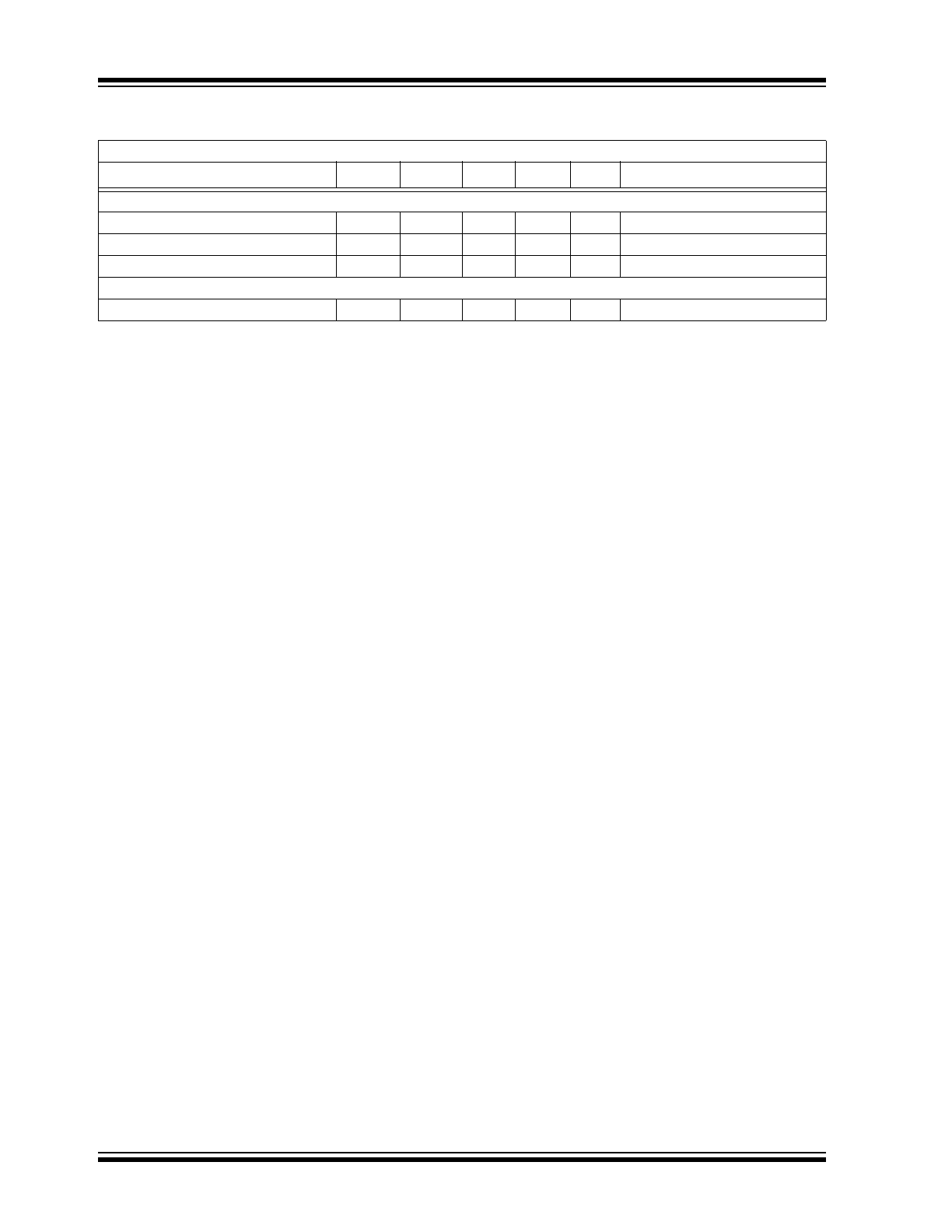
TEMPERATURE CHARACTERISTICS
Electrical Specifications: Unless otherwise indicated, V
DD
= +2.7V to +5.5V, V
SS
= GND.
Parameters
Sym
Min
Typ
Max
Units
Conditions
Temperature Ranges
Specified Temperature Range
T
A
-40
—
+125
°C
Operating Temperature Range
T
A
-40
—
+125
°C
Storage Temperature Range
T
A
-65
—
+150
°C
Thermal Package Resistances
Thermal Resistance, 6L-SC70
JA
—
207
—
°C/W
Note 1
Note 1:
Package Power Dissipation (P
DIS
) is calculated as follows:
P
DIS
= (T
J
- T
A
) /
JA
,
where: T
J
= Junction Temperature, T
A
= Ambient Temperature.