
2015 Microchip Technology Inc.
DS20005393B-page 1
MCP39F511
Features
• Power Monitoring Accuracy Capable of 0.1%
Error Across 4000:1 Dynamic Range
• Built-In Calculations on Fast 16-Bit Processing
Core
- Active, Reactive, Apparent Power
- True RMS Current, RMS Voltage
- Line Frequency, Power Factor
• 64-bit Wide Import and Export Active Energy
Accumulation Registers
• 64-bit Four Quadrant Reactive Energy
Accumulation Registers
• Signed Active and Reactive Power Outputs
• Dedicated Zero Crossing Detection (ZCD) Pin
Output with Less than 200 µs Latency
• Dedicated PWM Output Pin with Programmable
Frequency and Duty Cycle
• Automatic Event Pin Control through Fast Voltage
Surge Detection Less than 5 ms Delay
• Two Wire Serial Protocol with Selectable Baud
Rate Up to 115.2 kbps using Universal
Asynchronous Receiver/Transmitter (UART)
• Four Independent Registers for Minimum and
Maximum Output Quantity Tracking
• Fast Calibration Routines and Simplified
Command Protocol
• 512 Bytes User-Accessible EEPROM through
Page Read/Write Commands
• Low-Drift Internal Voltage Reference, 10 ppm/°C
Typical
• 28-lead 5x5 QFN Package
• Extended Temperature Range -40°C to +125°C
Applications
• Power Monitoring for Home Automation
• Industrial Lighting Power Monitoring
• Real-Time Measurement of Input Power for
AC/DC Supplies
• Intelligent Power Distribution Units
Description
The MCP39F511 is a highly integrated, complete
single-phase power-monitoring IC designed for
real-time measurement of input power for
AC/DC power supplies, power distribution units,
consumer and industrial applications. It includes
dual-channel Delta-Sigma ADCs, a 16-bit calculation
engine, EEPROM and a flexible 2-wire interface. An
integrated low-drift voltage reference with 10 ppm/°C in
addition to 94.5 dB of SINAD performance on each
measurement channel allows for better than 0.1%
accurate designs across a 4000:1 dynamic range.
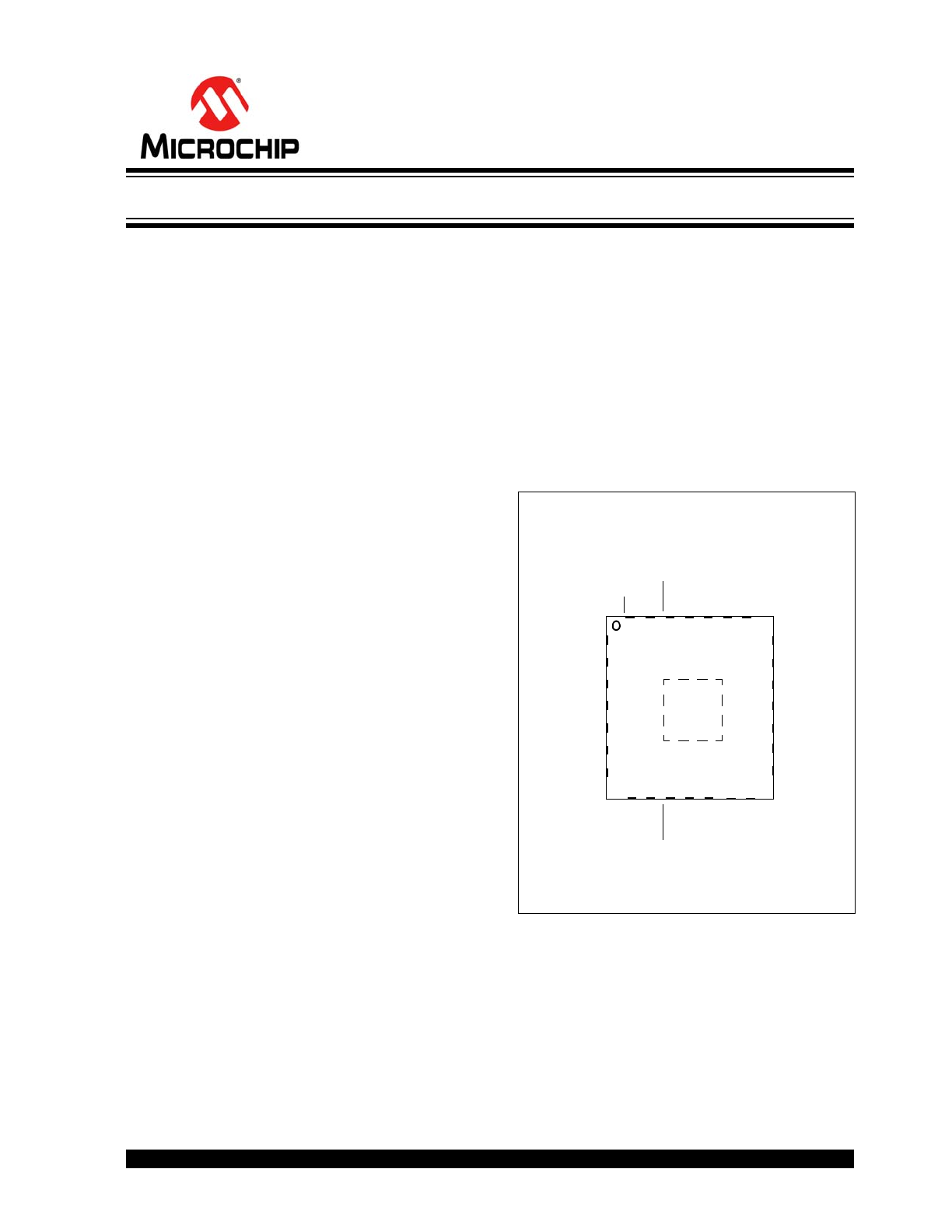
Package Types
1
25
2
3
4
5
8
9 10 11 12
21
20
19
18
17
28 27 26
24
EVENT1
NC
UART_RX
COMMON
A
NC
NC
NC
AV
DD
UAR
T
_
T
X
RESET
DV
DD
D
GN
D
MC
L
R
EP
29
6
7
OSCI
OSCO
13 14
CO
M
M
ON
B
PWM
16
15
23 22
REF
IN+/O
UT
ZC
D
I1+
I1-
V1-
V1+
AN_IN
A
GND
D
GN
D
EVENT2
DR
MCP39F511
5x5 QFN*
*Includes Exposed Thermal Pad (EP);
see
Table 3-1
.
Power-Monitoring IC with Calculation and Energy Accumulation
MCP39F511
DS20005393B-page 2
2015 Microchip Technology Inc.
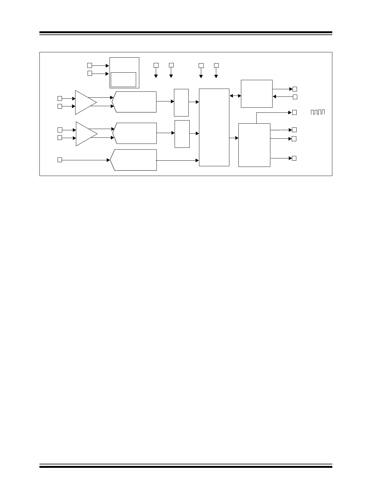
Functional Block Diagram
24-bit Delta-Sigma
Multi-level
+
-
SI
NC
3
Di
gi
ta
l Fi
lter
Modulator ADC
PGA
I1+
I1-
24-bit Delta-Sigma
Multi-level
+
-
SI
NC
3
D
ig
ita
l F
ilte
r
Modulator ADC
PGA
V1+
V1-
16-BIT
CORE
Calculation
Engine
(CE)
Digital Outputs
UART
Serial
Interface
UART_TX
UART_RX
EVENT1
FLASH
10-bit SAR
ADC
OSCI
OSCO
Timing
Generation
Internal
Oscillator
Generation
AV
DD
A
GND
DV
DD
D
GND
EVENT2
PWM
ZCD
AN_IN
2015 Microchip Technology Inc.
DS20005393B-page 3
MCP39F511
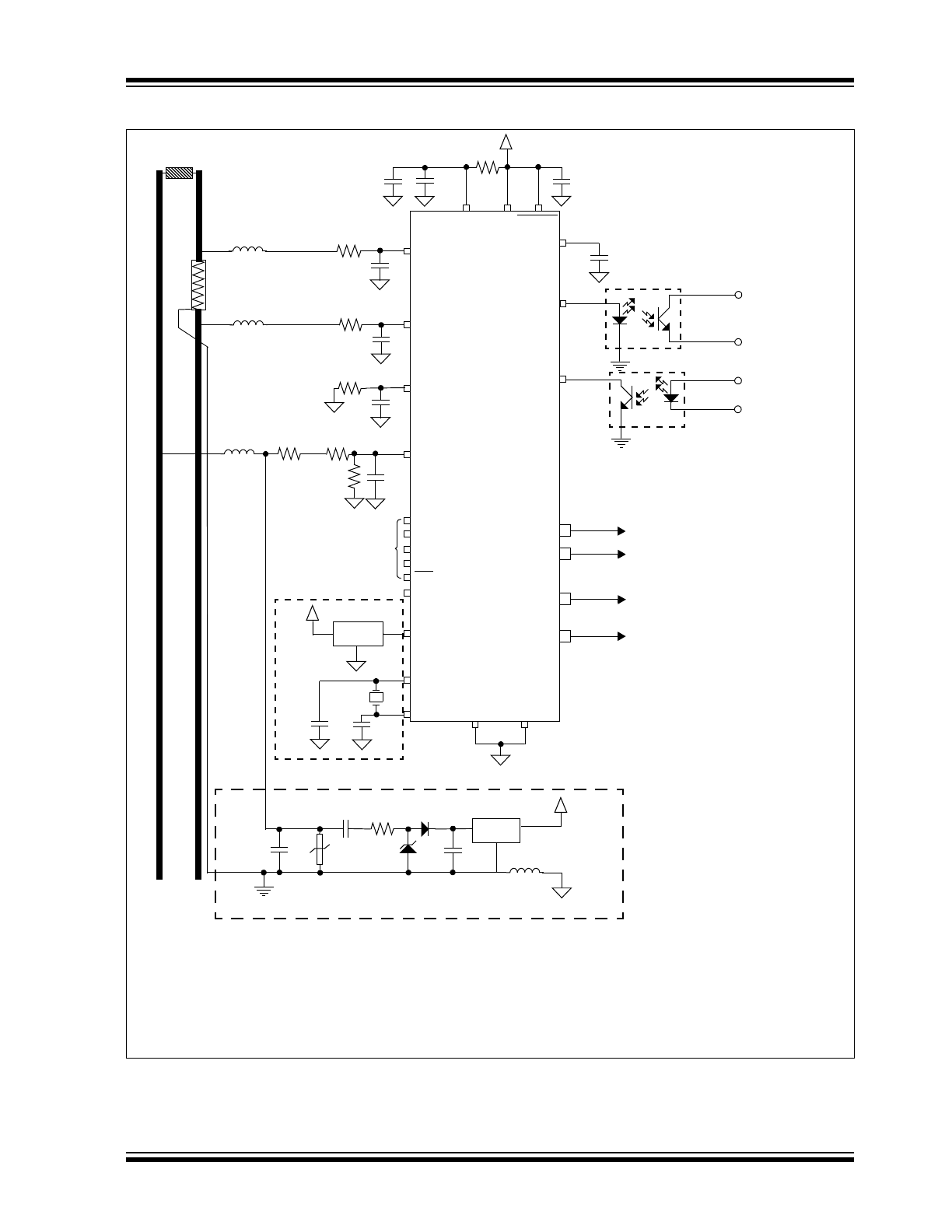
MCP39F511 Typical Application – Single Phase, Two-Wire Application Schematic
D
GND
OSCO
OSCI
DV
DD
RESET
AV
DD
I1+
I1-
V1-
V1+
NC
NC
NC
REFIN/OUT+
A
GND
COMMON
A,B
NC
LOAD
+3.3V
N
L
MCP1754
+3.3V
A
GND
D
GND
+
-
33 nF
33 nF
33 nF
1 k
1 k
1 k
499 k
1 k
4 MHz
22 pF
22 pF
33 nF
0.01 µF
0.47µ F 470
470 µF
10
1 µF
0.1 µF
0.1 µF
0.1 µF
AN_IN
2 m
Leave Floating
N.C.
MCP9700A
(OPTIONAL)
+3.3V
to MCU UART
to MCU UART
UART_RX
UART_TX
DR
(OPTIONAL)
Connect on PCB
EVENT1
ZCD
EVENT2
PWM
MCP39F511
499 k
Note 1:
The MCP39F511 demonstration board uses a switching power supply, however a low-cost
capacitive-based supply, as shown here, is sufficient for many applications.
2:
The external sensing components shown here, a 2 mΩ shunt, two 499 kΩ and 1 kΩ resistors for the
1000:1 voltage divider, are specifically chosen to match the default values for the calibration registers
defined in
Section 6.0 “Register Descriptions”
. By choosing low-tolerance components of these
values (e.g. 1% tolerance), measurement accuracy in the 2-3% range can be achieved with zero
calibration. See
Section 9.0 “MCP39F511 Calibration”
for more information.
MCP39F511
DS20005393B-page 4
2015 Microchip Technology Inc.
1.0
ELECTRICAL
CHARACTERISTICS
Absolute Maximum Ratings †
DV
DD
.................................................................. -0.3 to +4.5V
AV
DD
.................................................................. -0.3 to +4.0V
Digital inputs and outputs w.r.t. A
GND
............... -0.3V to +4.0V
Analog Inputs (I+,I-,V+,V-) w.r.t. A
GND
...................-2V to +2V
V
REF
input w.r.t. A
GND
........................ ....-0.6V to AV
DD
+0.6V
Maximum Current out of D
GND
pin..............................300 mA
Maximum Current into DV
DD
pin.................................250 mA
Maximum Output Current Sunk by Digital IO ................25 mA
Maximum Current Sourced by Digital IO.......................25 mA
Storage temperature .....................................-65°C to +150°C
Ambient temperature with power applied......-40°C to +125°C
Soldering temperature of leads (10 seconds) ............. +300°C
ESD on the analog inputs (HBM,MM) .................4.0 kV, 200V
ESD on all other pins (HBM,MM) ........................4.0 kV, 200V
† Notice:
Stresses above those listed under “Maximum
Ratings” may cause permanent damage to the device.
This is a stress rating only and functional operation of
the device at those or any other conditions above those
indicated in the operation listings of this specification is
not implied. Exposure to maximum rating conditions for
extended periods may affect device reliability.
1.1
Specifications
TABLE 1-1:
ELECTRICAL CHARACTERISTICS
Electrical Specifications:
Unless otherwise indicated, all parameters apply at AV
DD,
DV
DD
= +2.7 to +3.6V, T
A
= -40°C to +125°C,
MCLK = 4 MHz, PGA GAIN = 1.
Characteristic
Sym.
Min.
Typ.
Max.
Units
Test Conditions
Power Measurement
Active Power (
Note 1
)
P
—
±0.1
—
%
4000:1 Dynamic Range
on Current Channel
(
Note 2
)
Reactive Power (
Note 1
)
Q
—
±0.1
—
%
4000:1 Dynamic Range
on Current Channel
(
Note 2
)
Apparent Power (
Note 1
)
S
—
±0.1
—
%
4000:1 Dynamic Range
on Current Channel
(
Note 2
)
Current RMS (
Note 1
)
I
RMS
—
±0.1
—
%
4000:1 Dynamic Range
on Current Channel
(
Note 2
)
Voltage RMS (
Note 1
)
V
RMS
—
±0.1
—
%
4000:1 Dynamic Range
on Voltage Channel
(
Note 2
)
Power Factor (
Note 1
)
—
±0.1
—
%
Line Frequency (
Note 1
)
LF
—
±0.1
—
%
Note 1:
Calculated from reading the register values with no averaging, single computation cycle with accumulation interval of 4
line cycles.
2:
Specification by design and characterization; not production tested.
3:
N = Value in the Accumulation Interval Parameter register. The default value of this register is 2 or T
CAL
= 80 ms for
50 Hz line.
4:
Applies to Voltage Sag and Voltage Surge events only.
5:
Applies to all gains. Offset and gain errors depend on the PGA gain setting. See
Section 2.0 “Typical Performance
Curves”
for typical performance.
6:
V
IN
= 1V
PP
= 353 mV
RMS
@ 50/60 Hz.
7:
Variation applies to internal clock and UART only. All calculated output quantities are temperature compensated to the
performance listed in the respective specification.
8:
Lower baud rates selectable only on system versions 0xFA14 and later.
2015 Microchip Technology Inc.
DS20005393B-page 5
MCP39F511
Calibration, Calculation and Event Detection Times
Auto-Calibration Time
t
CAL
—
2
N
x (1/f
LINE
)
—
ms
Note 3
Minimum Time
for Voltage Surge/Sag
Detection
t
AC_SASU
—
see
Section 7.0
—
ms
Note 4
24-Bit Delta-Sigma ADC Performance
Analog Input
Absolute Voltage
V
IN
-1
—
+1
V
Analog Input
Leakage Current
A
IN
—
1
—
nA
Differential Input
Voltage Range
(I1+ – I1-),
(V1+ – V1-)
-600/GAIN
—
+600/GAIN
mV
V
REF
= 1.2V,
proportional to V
REF
Offset Error
V
OS
-1
—
+1
mV
Offset Error Drift
—
0.5
—
µV/°C
Gain Error
GE
-4
—
+4
%
Note 5
Gain Error Drift
—
1
—
ppm/°C
Differential Input
Impedance
Z
IN
232
—
—
k
G = 1
142
—
—
k
G = 2
72
—
—
k
G = 4
38
—
—
k
G = 8
36
—
—
k
G = 16
33
—
—
k
G = 32
Signal-to-Noise
and Distortion Ratio
SINAD
92
94.5
—
dB
Note 6
Total Harmonic Distortion
THD
—
-106.5
-103
dBc
Note 6
Signal-to-Noise Ratio
SNR
92
95
—
dB
Note 6
Spurious Free
Dynamic Range
SFDR
—
111
—
dB
Note 6
Crosstalk
CTALK
—
-122
—
dB
AC Power
Supply Rejection Ratio
AC PSRR
—
-73
—
dB
AV
DD
and
DV
DD
= 3.3V + 0.6V
PP
,
100 Hz, 120 Hz, 1 kHz
DC Power
Supply Rejection Ratio
DC PSRR
—
-73
—
dB
AV
DD
and DV
DD
= 3.0 to
3.6V
TABLE 1-1:
ELECTRICAL CHARACTERISTICS (CONTINUED)
Electrical Specifications:
Unless otherwise indicated, all parameters apply at AV
DD,
DV
DD
= +2.7 to +3.6V, T
A
= -40°C to +125°C,
MCLK = 4 MHz, PGA GAIN = 1.
Characteristic
Sym.
Min.
Typ.
Max.
Units
Test Conditions
Note 1:
Calculated from reading the register values with no averaging, single computation cycle with accumulation interval of 4
line cycles.
2:
Specification by design and characterization; not production tested.
3:
N = Value in the Accumulation Interval Parameter register. The default value of this register is 2 or T
CAL
= 80 ms for
50 Hz line.
4:
Applies to Voltage Sag and Voltage Surge events only.
5:
Applies to all gains. Offset and gain errors depend on the PGA gain setting. See
Section 2.0 “Typical Performance
Curves”
for typical performance.
6:
V
IN
= 1V
PP
= 353 mV
RMS
@ 50/60 Hz.
7:
Variation applies to internal clock and UART only. All calculated output quantities are temperature compensated to the
performance listed in the respective specification.
8:
Lower baud rates selectable only on system versions 0xFA14 and later.
MCP39F511
DS20005393B-page 6
2015 Microchip Technology Inc.
DC Common
Mode Rejection Ratio
DC CMRR
—
-105
—
dB
V
CM
varies
from -1V to +1V
10-Bit SAR ADC Performance for Temperature Measurement
Resolution
N
R
—
10
—
bits
Absolute Input Voltage
V
IN
D
GND
- 0.3
—
D
VDD
+ 0.3
V
Recommended
Impedance of
Analog Voltage Source
R
IN
—
—
2.5
k
Integral Nonlinearity
I
NL
—
±1
±2
LSb
Differential Nonlinearity
D
NL
—
±1
±1.5
LSb
Gain Error
G
ERR
—
±1
±3
LSb
Offset Error
E
OFF
—
±1
±2
LSb
Temperature
Measurement Rate
—
f
LINE
/2
N
—
sps
Note 7
Clock and Timings
UART Baud Rate
UDB
1.2
(
8
)
—
115.2
kbps
See
Section 3.2
for
protocol details
Master Clock
and Crystal Frequency
f
MCLK
-2%
4
+2%
MHz
Capacitive Loading
on OSCO pin
COSC2
—
—
15
pF
When an external clock is
used to drive the device
Internal Oscillator
Tolerance
f
INT_OSC
—
2
—
%
-40 to +85°C only
(
Note 7
)
Internal Voltage Reference
Internal Voltage
Reference Tolerance
V
REF
-2%
1.2
+2%
V
Temperature Coefficient
TCV
REF
—
10
—
ppm/°C T
A
= -40°C to +85°C,
V
REFEXT
= 0
Output Impedance
ZOUTV
REF
—
2
—
k
Current, V
REF
AI
DD
V
REF
—
40
—
µA
Voltage Reference Input
Input Capacitance
—
—
10
pF
Absolute Voltage on
V
REF+
Pin
V
REF+
A
GND
+ 1.1V
—
A
GND
+ 1.3V
V
TABLE 1-1:
ELECTRICAL CHARACTERISTICS (CONTINUED)
Electrical Specifications:
Unless otherwise indicated, all parameters apply at AV
DD,
DV
DD
= +2.7 to +3.6V, T
A
= -40°C to +125°C,
MCLK = 4 MHz, PGA GAIN = 1.
Characteristic
Sym.
Min.
Typ.
Max.
Units
Test Conditions
Note 1:
Calculated from reading the register values with no averaging, single computation cycle with accumulation interval of 4
line cycles.
2:
Specification by design and characterization; not production tested.
3:
N = Value in the Accumulation Interval Parameter register. The default value of this register is 2 or T
CAL
= 80 ms for
50 Hz line.
4:
Applies to Voltage Sag and Voltage Surge events only.
5:
Applies to all gains. Offset and gain errors depend on the PGA gain setting. See
Section 2.0 “Typical Performance
Curves”
for typical performance.
6:
V
IN
= 1V
PP
= 353 mV
RMS
@ 50/60 Hz.
7:
Variation applies to internal clock and UART only. All calculated output quantities are temperature compensated to the
performance listed in the respective specification.
8:
Lower baud rates selectable only on system versions 0xFA14 and later.
2015 Microchip Technology Inc.
DS20005393B-page 7
MCP39F511
Power Specifications
Operating Voltage
AV
DD
, DV
DD
2.7
—
3.6
V
DV
DD
Start Voltage
to Ensure Internal
Power-On Reset Signal
V
POR
D
GND
—
0.7
V
DV
DD
Rise Rate to
Ensure Internal
Power-On Reset Signal
SDV
DD
0.05
—
—
V/ms
0 – 3.3V in 0.1s, 0 – 2.5V
in 60 ms
AV
DD
Start Voltage to
Ensure Internal
Power-On Reset Signal
V
POR
A
GND
—
2.1
V
AV
DD
Rise Rate to
Ensure Internal Power On
Reset Signal
SAV
DD
0.042
—
—
V/ms
0 – 2.4V in 50 ms
Operating Current
I
DD
—
13
—
mA
Data EEPROM Memory
Cell Endurance
EPS
100,000
—
—
E/W
Self-Timed
Write Cycle Time
T
IWD
—
4
—
ms
Number of Total
Write/Erase Cycles
Before Refresh
R
REF
—
10,000,000
—
E/W
Characteristic Retention
T
RETDD
40
—
—
years
Provided no other
specifications are violated
Supply Current during
Programming
I
DDPD
—
7
—
mA
TABLE 1-1:
ELECTRICAL CHARACTERISTICS (CONTINUED)
Electrical Specifications:
Unless otherwise indicated, all parameters apply at AV
DD,
DV
DD
= +2.7 to +3.6V, T
A
= -40°C to +125°C,
MCLK = 4 MHz, PGA GAIN = 1.
Characteristic
Sym.
Min.
Typ.
Max.
Units
Test Conditions
Note 1:
Calculated from reading the register values with no averaging, single computation cycle with accumulation interval of 4
line cycles.
2:
Specification by design and characterization; not production tested.
3:
N = Value in the Accumulation Interval Parameter register. The default value of this register is 2 or T
CAL
= 80 ms for
50 Hz line.
4:
Applies to Voltage Sag and Voltage Surge events only.
5:
Applies to all gains. Offset and gain errors depend on the PGA gain setting. See
Section 2.0 “Typical Performance
Curves”
for typical performance.
6:
V
IN
= 1V
PP
= 353 mV
RMS
@ 50/60 Hz.
7:
Variation applies to internal clock and UART only. All calculated output quantities are temperature compensated to the
performance listed in the respective specification.
8:
Lower baud rates selectable only on system versions 0xFA14 and later.
MCP39F511
DS20005393B-page 8
2015 Microchip Technology Inc.
TABLE 1-2:
SERIAL DC CHARACTERISTICS
Electrical Specifications:
Unless otherwise indicated, all parameters apply at AV
DD,
DV
DD
= +2.7 to+ 3.6V,
T
A
= -40°C to +125°C, MCLK = 4 MHz
Characteristic
Sym.
Min.
Typ.
Max.
Units
Test Conditions
High-Level Input Voltage
V
IH
0.8 DV
DD
—
DV
DD
V
Low-Level Input Voltage
V
IL
0
—
0.2 DV
DD
V
High-Level Output Voltage
V
OH
3
—
—
V
I
OH
= -3.0 mA, V
DD
= 3.6V
Low-Level Output Voltage
V
OL
—
—
0.4
V
I
OL
= 4.0 mA, V
DD
= 3.6V
Input Leakage Current
I
LI
—
—
1
µA
0.050
0.100
Digital Output pins only
(ZCD, PWM, EVENT1,
EVENT2)
TABLE 1-3:
TEMPERATURE SPECIFICATIONS
Electrical Specifications:
Unless otherwise indicated, all parameters apply at AV
DD,
DV
DD
= +2.7 to +3.6V.
Parameters
Sym.
Min.
Typ.
Max.
Units
Conditions
Temperature Ranges
Operating Temperature Range
T
A
-40
—
+125
°C
Storage Temperature Range
T
A
-65
—
+150
°C
Thermal Package Resistances
Thermal Resistance, 28LD 5x5 QFN
JA
—
36.9
—
°C/W
2015 Microchip Technology Inc.
DS20005393B-page 9
MCP39F511
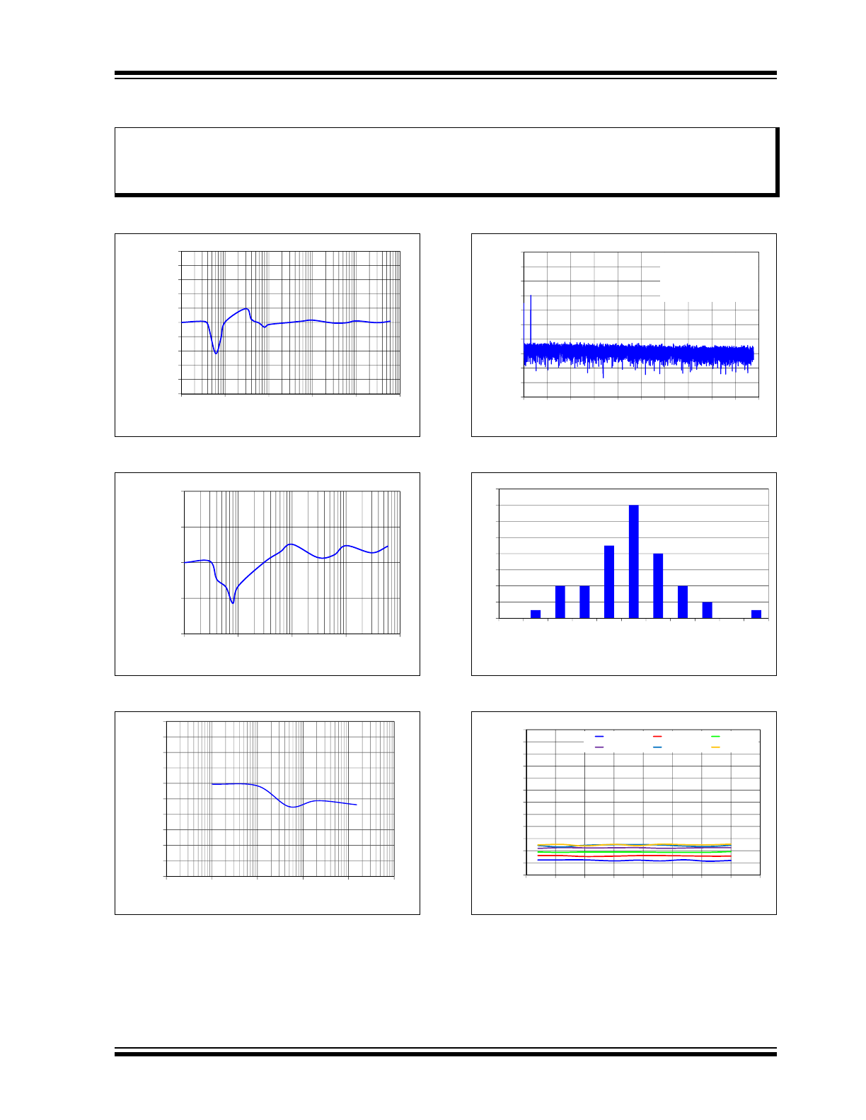
2.0
TYPICAL PERFORMANCE CURVES
Note:
Unless otherwise indicated, AV
DD
= +3.3V, DV
DD
= +3.3V, T
A
= +25°C, GAIN = 1, V
IN
= -0.5 dBFS at 60 Hz
.
FIGURE 2-1:
Active Power, Gain = 1.
FIGURE 2-2:
RMS Current, Gain = 1.
FIGURE 2-3:
Energy, Gain = 8.
FIGURE 2-4:
Spectral Response.
FIGURE 2-5:
THD Histogram.
FIGURE 2-6:
THD vs. Temperature.
Note:
The graphs and tables provided following this note are a statistical summary based on a limited number of
samples and are provided for informational purposes only. The performance characteristics listed herein
are not tested or guaranteed. In some graphs or tables, the data presented may be outside the specified
operating range (e.g., outside specified power supply range) and therefore outside the warranted range.
-0.50%
-0.40%
-0.30%
-0.20%
-0.10%
0.00%
0.10%
0.20%
0.30%
0.40%
0.50%
0.01
0.1
1
10
100
1000
Measurement Error
(%)
Current Channel Input Amplitude (mV
PEAK
)
-0.100%
-0.050%
0.000%
0.050%
0.100%
0.1
1
10
100
1000
RMS Current Error
(%)
Input Voltage RMS (mV
PP
)
-1
-0.8
-0.6
-0.4
-0.2
0
0.2
0.4
0.6
0.8
1
1
10
100
1000
10000
100000
Energy
Accumulation Error (%
)
Energy Accumulation (Watt-Hours)
-200
-180
-160
-140
-120
-100
-80
-60
-40
-20
0
0
200
400
600
800 1000 1200 1400 1600 1800 2000
Am
plitude (dB)
Frequency (Hz)
f
IN
= -60 dBFS @ 60 Hz
f
D
= 3.9 ksps
16384 pt FFT
OSR = 256
-1
07.3
-1
07.1
-1
07.0
-1
06.8
-1
06.7
-1
06.5
-1
06.4
-1
06.2
-1
06.1
-1
05.9
-1
05.8
Frequency
of
Occurr
ence
Total Harmonic Distortion (-dBc)
-120
-110
-100
-90
-80
-70
-60
-50
-40
-30
-20
-10
0
-50
-25
0
25
50
75
100
125
150
Total H
D
rmonic Distortion
(dBc)
Temperature (°C)
G = 1
G = 2
G = 4
G = 8
G = 16
G = 32
MCP39F511
DS20005393B-page 10
2015 Microchip Technology Inc.
Note:
Unless otherwise indicated, AV
DD
= 3.3V, DV
DD
= 3.3V, T
A
= +25°C, GAIN = 1, V
IN
= -0.5 dBFS at 60 Hz
.
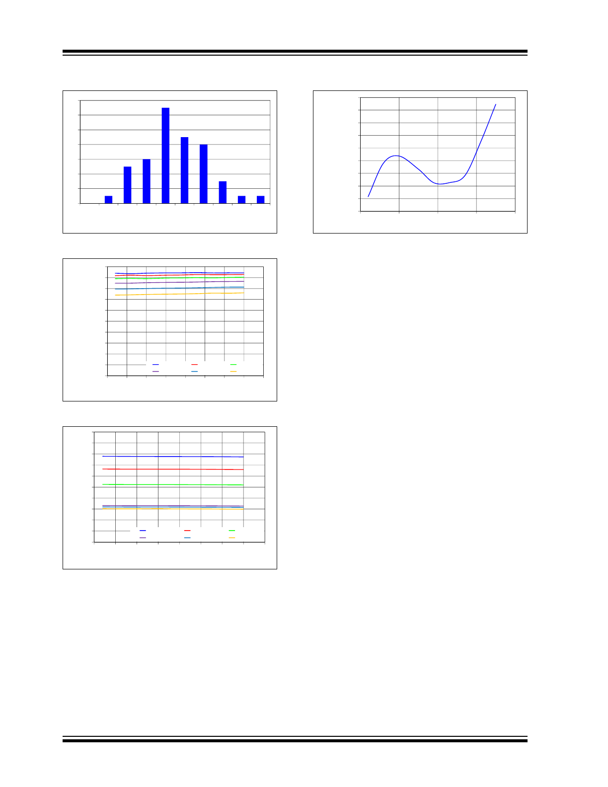
FIGURE 2-7:
SNR Histogram.
FIGURE 2-8:
SINAD vs. Temperature.
FIGURE 2-9:
Gain Error vs. Temperature.
FIGURE 2-10:
Internal Voltage Reference
vs. Temperature.
94.2 94.3 94.5 94.6 94.8 94.9 95.1 95.2 95.4 95.5
Frequency of
Occurrence
Signal-to-Noise and Distortion Ratio (dB)
0
10
20
30
40
50
60
70
80
90
100
-50
-25
0
25
50
75
100
125
150
Signal
-to-Noise and
Distortion
R
a
tio (d
B)
Temperature (°C)
G = 1
G = 2
G = 4
G = 8
G = 16
G = 32
-5
-4
-3
-2
-1
0
1
2
3
4
5
-50
-25
0
25
50
75
100
125
150
Gain Error
(%
)
Temperature (°C)
G = 1
G = 2
G = 4
G = 8
G = 16
G = 32
1.1999
1.2000
1.2001
1.2002
1.2003
1.2004
1.2005
1.2006
1.2007
1.2008
-50
0
50
100
150
Internal V
o
ltage Reference
(V)
Temperature (C)