
2013 Microchip Technology Inc.
DS20005256A-page 1
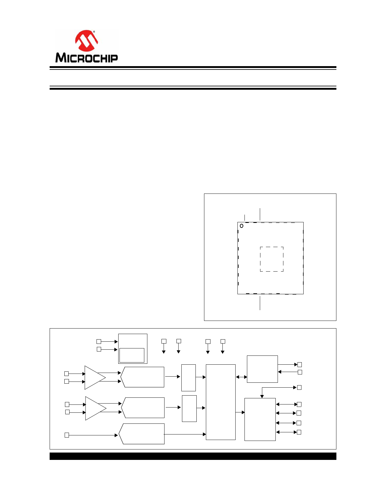
MCP39F501
Features:
• Power Monitoring Accuracy capable of 0.1% error
across 4000:1 dynamic range
• Fast Calibration Routines
• Programmable Event Notifications such as over-
current and voltage sag, surge protection
• 512 bytes User-accessible EEPROM through
page read/write commands
• Non-volatile On-chip Memory, no external
memory required
• Built-in calculations on fast 16-bit processing core
- Active, Reactive and Apparent Power
- True RMS Current, RMS Voltage
- Line Frequency, Power Factor
• Two-Wire Serial Protocol using a 2-wire Universal
Asynchronous Receiver/Transmitter (UART) inter-
face supporting multiple devices on a single bus
• Low-Drift Internal Voltage Reference, 10 ppm/°C
typical
• 28-lead 5x5 QFN package
• Extended Temperature Range -40°C to +125°C
Applications:
• Real-time Measurement of Input Power for
AC/DC supplies
• Intelligent Power Distribution Units
Description:
The MCP39F501 is a highly integrated, single-phase
power-monitoring IC designed for real-time
measurement of input power for AC/DC power
supplies, power distribution units and industrial
applications. It includes dual-channel delta sigma
ADCs, a 16-bit calculation engine, EEPROM and a
flexible 2-wire interface. An integrated low-drift voltage
reference with 10 ppm/°C in addition to 94.5 dB of
SINAD performance on each measurement channel
allows for better than 0.1% accurate designs across a
4000:1 dynamic range.
Package Type
Functional Block Diagram
1
25
2
3
4
5
8
9
10 11 12
21
20
19
18
17
28 27 26
24
MODE/DIR
NC
UART_RX
COMMON
A
NC
NC
NC
AV
DD
UAR
T
_
T
X
RESET
DV
DD
D
GN
D
MC
L
R
EP
29
6
7
OSCI
OSCO
13 14
CO
M
M
ON
B
A
0
/D
IO0
16
15
23 22
REF
IN+/O
UT
DIO3
I1+
I1-
V1-
V1+
AN_IN/DIO2
A
GND
D
GN
D
A1/DIO1
DR
MCP39F501
5x5 QFN*
* Includes Exposed
Thermal Pad (EP); see
Table 3-1
.
24-bit Delta Sigma
Multi-level
+
-
SI
N
C
3
Di
gi
ta
l Fi
lt
e
r
Modulator ADC
PGA
I1+
I1-
24-bit Delta Sigma
Multi-level
+
-
SI
NC
3
D
igi
ta
l F
ilt
er
Modulator ADC
PGA
V1+
V1-
16-BIT
CORE
Calculation
Engine
(CE)
Configurable
Digital Outputs
UART
Serial
Interface
UART_TX
UART_RX
A0/DIO0
FLASH
10-bit SAR
ADC
AN_IN/DIO2
OSCI
OSCO
Timing
Generation
Internal
Oscillator
Generation
AV
DD
A
GND
DV
DD
D
GND
A1/DIO1
MODE/DIR
DIO3
AN_IN/DIO2
Single-Phase, Power-Monitoring IC with Calculation and Event Detection
MCP39F501
DS20005256A-page 2
2013 Microchip Technology Inc.
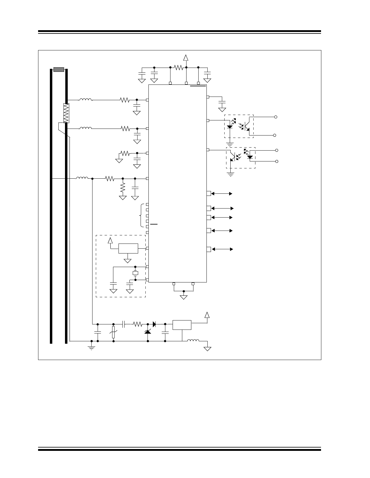
MCP39F501 Typical Application – Single Phase, Two-Wire Application Schematic
D
GND
OSCO
OSCI
DV
DD
RESET
AV
DD
I1+
I1-
V1-
V1+
NC
NC
NC
REFIN/OUT+
A
GND
COMMON
A,B
NC
LOAD
+3.3V
N
L
MCP1754
+3.3V
A
GND
D
GND
+
-
33 nF
33 nF
33 nF
1 k
1 k
1 k
720 k
1 k
4 MHz
22 pF
22 pF
33 nF
0.01 µF
0.47 µ F 470
470 µF
10
1 µF
0.1 µF
0.1 µF
0.1 µF
0.5 m
1 m
TEMPIN/DIO2
2 m
Leave Floating
N.C.
MCP9700A
(OPTIONAL)
+3.3V
to MCU UART
to MCU UART
UART_RX
UART_TX
DR
(OPTIONAL)
Connect on PCB
A0/DIO0
DIO3
A1/DIO1
MODE/DIR
DIO2
Address setting for multiple devices
or
Alarm with Event Functions
MCP39F501
4 m
2013 Microchip Technology Inc.
DS20005256A-page 3
MCP39F501
1.0
ELECTRICAL
CHARACTERISTICS
Absolute Maximum Ratings †
DV
DD
.....................................................................-0.3 to 4.5V
AV
DD
.....................................................................-0.3 to 4.0V
Digital inputs and outputs w.r.t. A
GND
................. -0.3V to 4.0V
Analog Inputs (I+,I-,V+,V-) w.r.t. A
GND
............... ....-2V to +2V
V
REF
input w.r.t. A
GND
.............................-0.6V to AV
DD
+0.6V
Maximum Current out of D
GND
pin..............................300 mA
Maximum Current into DV
DD
pin.................................250 mA
Maximum Output Current Sunk by Digital IO ................25 mA
Maximum Current Sourced by Digital IO.......................25 mA
Storage temperature .....................................-65°C to +150°C
Ambient temperature with power applied......-40°C to +125°C
Soldering temperature of leads (10 seconds) ............. +300°C
ESD on the analog inputs (HBM,MM) ................. 4.0 kV, 200V
ESD on all other pins (HBM,MM) ........................ 4.0 kV, 200V
† Notice: Stresses above those listed under “Maximum
Ratings” may cause permanent damage to the device.
This is a stress rating only and functional operation of
the device at those or any other conditions above those
indicated in the operation listings of this specification is
not implied. Exposure to maximum rating conditions for
extended periods may affect device reliability.
1.1
Specifications
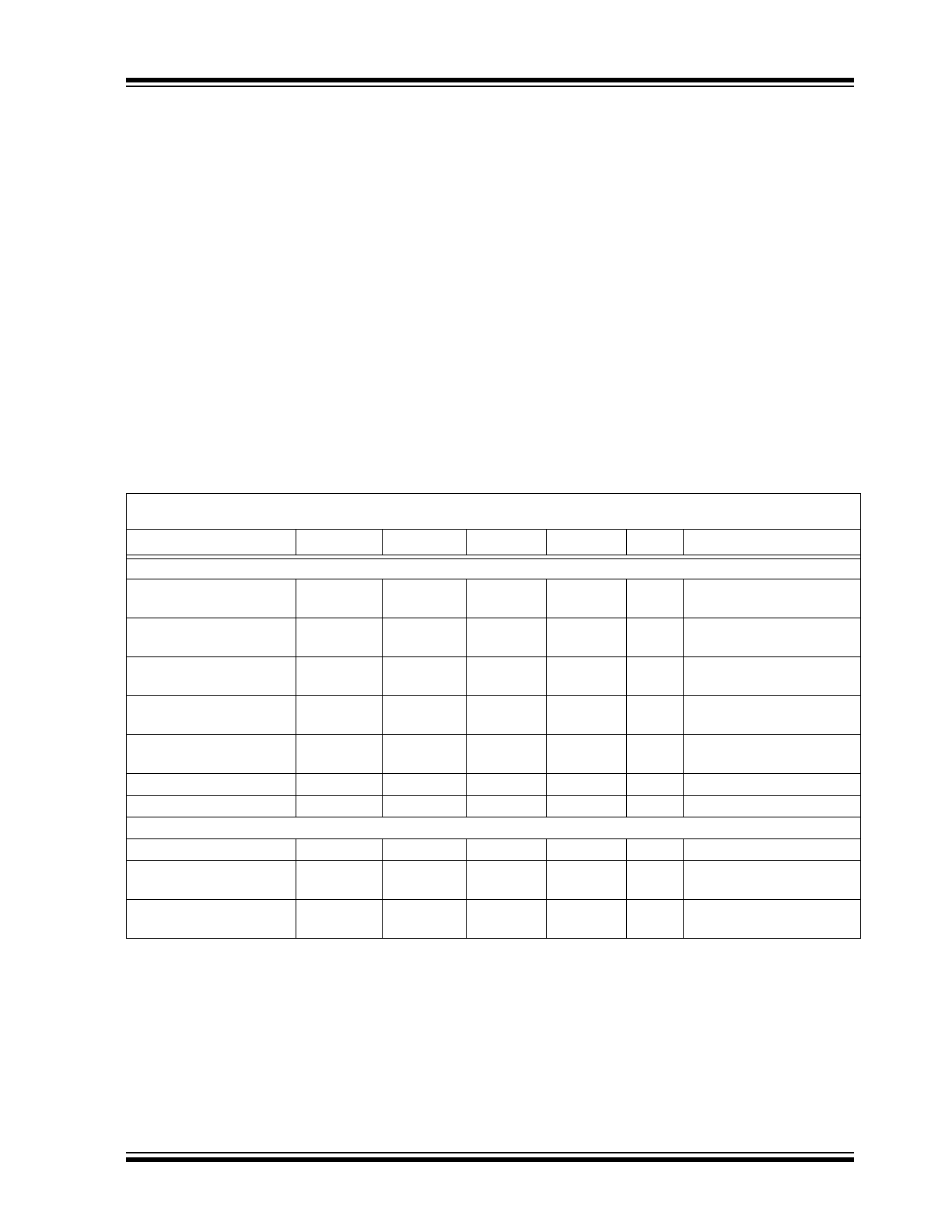
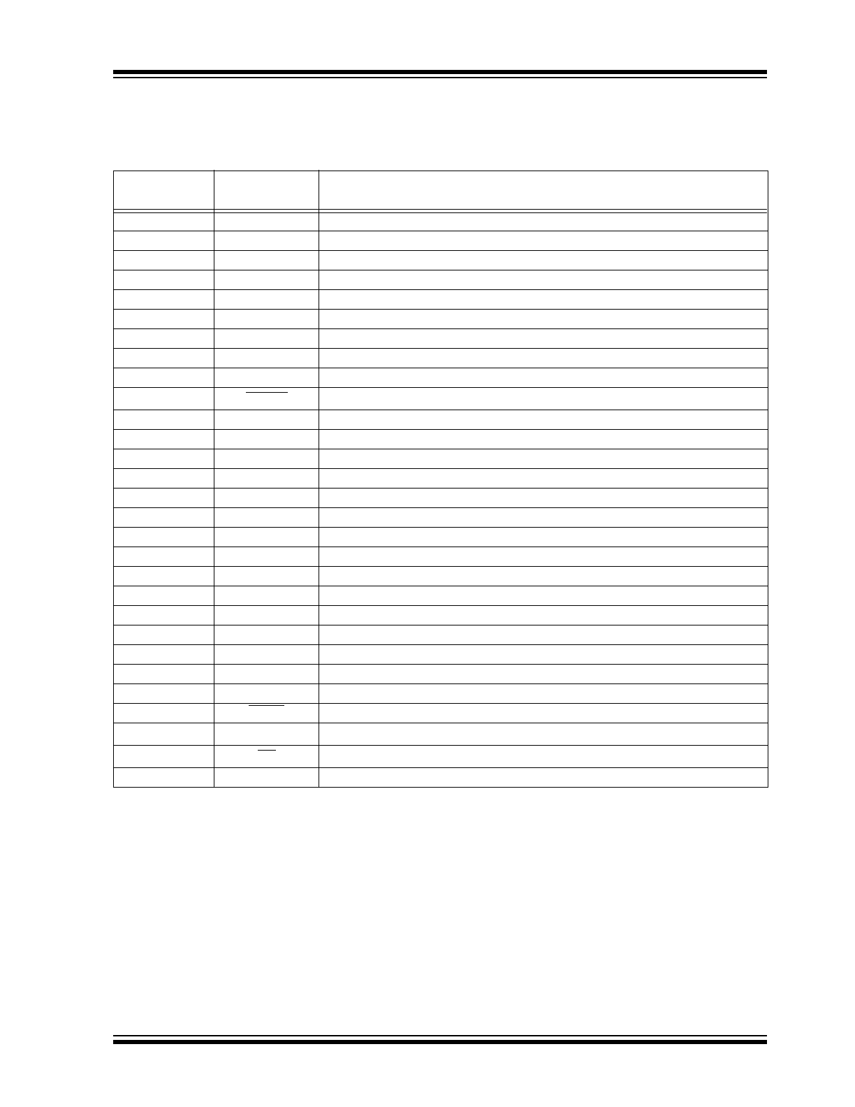
TABLE 1-1:
ELECTRICAL CHARACTERISTICS
Electrical Specifications: Unless otherwise indicated, all parameters apply at AV
DD,
DV
DD
= 2.7 to 3.6 V, T
A
= -40°C to +125°C,
MCLK = 4 MHz, PGA GAIN = 1.
Characteristic
Sym.
Min.
Typ.
Max.
Units
Test Conditions
Power Measurement
Active Power (
Note 2
)
P
—
±0.1
—
%
4000:1 Dynamic Range on
Current Channel (
Note 1
)
Reactive Power (
Note 2
)
Q
—
±0.1
—
%
4000:1 Dynamic Range on
Current Channel (
Note 1
)
Apparent Power (
Note 2
)
S
—
±0.1
—
%
4000:1 Dynamic Range on
Current Channel (
Note 1
)
Current RMS (
Note 2
)
I
RMS
—
±0.1
—
%
4000:1 Dynamic Range on
Current Channel (
Note 1
)
Voltage RMS (
Note 2
)
V
RMS
—
±0.1
—
%
4000:1 Dynamic Range on
Voltage Channel (
Note 1
)
Power Factor (
Note 2
)
—
±0.1
—
%
Line Frequency (
Note 2
)
V
RMS
—
±0.1
—
%
Calibration, Calculation and Event Detection Times
Auto-Calibration Time
t
CAL
—
2
N
x (1/f
LINE
)
—
ms
Note 7
Minimum Calculation
and Event Detection Time
t
CALC_EVENT
2
N
x (1/f
LINE
)
—
—
ms
Minimum Time
for Voltage Sag Detection
t
AC_DROP
—
see
Section 7.7
—
ms
Note 4
Note 1:
Specification by design and characterization; not production tested.
2:
Calculated from reading the register values.
3:
V
IN
= 1V
PP
= 353 mV
RMS
@ 50/60 Hz.
4:
Applies to Voltage Sag and Voltage Surge Events Only.
5:
Variation applies to internal clock and UART only. All calculated output quantities are temperature compensated to the
performance listed in the respective specification.
6:
Applies to all gains. Offset and gain errors depend on the PGA gain setting. See
Section 2.0 “Typical Performance
Curves”
for typical performance.
7:
N = Value in the AccumulationInternalParameter register (0x005A). The default value of this register is 2 or T
CAL
= 80 ms
for 50 Hz line.
MCP39F501
DS20005256A-page 4
2013 Microchip Technology Inc.
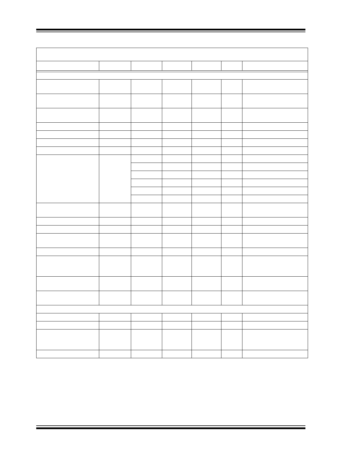
24-Bit Delta Sigma ADC Performance
Analog Input
Absolute Voltage
V
IN
-1
—
+1
V
Analog Input
Leakage Current
A
IN
—
1
—
nA
Differential Input
Voltage Range
(I1+ – I1-),
(V1+ – V1-)
-600/GAIN
—
+600/GAIN
mV
V
REF
= 1.2V,
proportional to V
REF
Offset Error
V
OS
-1
—
+1
mV
Offset Error Drift
—
0.5
—
µV/°C
Gain Error
GE
-4
—
+4
%
Note 6
Gain Error Drift
—
1
—
ppm/°C
Differential Input
Impedance
Z
IN
232
—
—
k
G = 1
142
—
—
k
G = 2
72
—
—
k
G = 4
38
—
—
k
G = 8
36
—
—
k
G = 16
33
—
—
k
G = 32
Signal-to-Noise
and Distortion Ratio
SINAD
92
94.5
—
dB
Note 3
Total Harmonic Distortion
THD
—
-106.5
-103
dBc
Note 3
Signal-to-Noise Ratio
SNR
92
95
—
dB
Note 3
Spurious Free
Dynamic Range
SFDR
—
111
—
dB
Note 3
Crosstalk
CTALK
—
-122
—
dB
AC Power
Supply Rejection Ratio
AC PSRR
—
-73
—
dB
AV
DD
and
DV
DD
= 3.3V + 0.6V
PP
,
100 Hz, 120 Hz, 1 kHz
DC Power
Supply Rejection Ratio
DC PSRR
—
-73
—
dB
AV
DD
and DV
DD
= 3.0 to
3.6V
DC Common
Mode Rejection Ratio
DC CMRR
—
-105
—
dB
V
CM
varies
from -1V to +1V
10-Bit SAR ADC Performance for Temperature Measurement
Resolution
N
R
—
10
—
bits
Absolute Input Voltage
V
IN
D
GND
- 0.3
—
D
GND
+ 0.3
V
Recommended
Impedance of
Analog Voltage Source
R
IN
—
—
2.5
k
Integral Non-Linearity
I
NL
—
±1
±2
LSb
TABLE 1-1:
ELECTRICAL CHARACTERISTICS (CONTINUED)
Electrical Specifications: Unless otherwise indicated, all parameters apply at AV
DD,
DV
DD
= 2.7 to 3.6 V, T
A
= -40°C to +125°C,
MCLK = 4 MHz, PGA GAIN = 1.
Characteristic
Sym.
Min.
Typ.
Max.
Units
Test Conditions
Note 1:
Specification by design and characterization; not production tested.
2:
Calculated from reading the register values.
3:
V
IN
= 1V
PP
= 353 mV
RMS
@ 50/60 Hz.
4:
Applies to Voltage Sag and Voltage Surge Events Only.
5:
Variation applies to internal clock and UART only. All calculated output quantities are temperature compensated to the
performance listed in the respective specification.
6:
Applies to all gains. Offset and gain errors depend on the PGA gain setting. See
Section 2.0 “Typical Performance
Curves”
for typical performance.
7:
N = Value in the AccumulationInternalParameter register (0x005A). The default value of this register is 2 or T
CAL
= 80 ms
for 50 Hz line.
2013 Microchip Technology Inc.
DS20005256A-page 5
MCP39F501
Differential Non-Linearity
D
NL
—
±1
±1.5
LSb
Gain Error
G
ERR
—
±1
±3
LSb
Offset Error
E
OFF
—
±1
±2
LSb
Temperature
Measurement Rate
—
f
LINE
/2
N
—
sps
Note 7
Clock and Timings
UART Baud Rate
UDB
—
4.8
—
kbps
See
Section 3.2
for
protocol details
Master Clock
and Crystal Frequency
f
MCLK
-2%
4
+2%
MHz
Capacitive Loading
on OSCO pin
COSC2
—
—
15
pF
When an external clock is
used to drive the device
Internal Oscillator
Tolerance
f
INT_OSC
—
2
—
%
-40 to +85°C only (
Note 5
)
Internal Voltage Reference
Internal Voltage
Reference Tolerance
V
REF
-2%
1.2
+2%
V
Temperature Coefficient
TCV
REF
—
10
—
ppm/°C T
A
= -40°C to +85°C,
VREFEXT = 0
Output Impedance
ZOUTV
REF
—
2
—
k
Current, V
REF
AI
DD
V
REF
—
40
—
µA
Voltage Reference Input
Input Capacitance
—
—
10
pF
Absolute Voltage on
V
REF+
Pin
V
REF+
A
GND
+ 1.1V
—
A
GND
+ 1.1V
V
Power Specifications
Operating Voltage
AV
DD
, DV
DD
2.7
—
3.6
V
DV
DD
Start Voltage
to Ensure Internal
Power-On Reset Signal
V
POR
D
GND
—
0.7
V
DV
DD
Rise Rate to
Ensure Internal
Power-On Reset Signal
SDV
DD
0.05
—
—
V/ms
0 – 3.3V in 0.1s, 0 – 2.5V
in 60 ms
AV
DD
Start Voltage to
Ensure Internal
Power-On Reset Signal
V
POR
A
GND
—
2.1
V
AV
DD
Rise Rate to
Ensure Internal Power On
Reset Signal
SAV
DD
0.042
—
—
V/ms
0 – 2.4V in 50 ms
TABLE 1-1:
ELECTRICAL CHARACTERISTICS (CONTINUED)
Electrical Specifications: Unless otherwise indicated, all parameters apply at AV
DD,
DV
DD
= 2.7 to 3.6 V, T
A
= -40°C to +125°C,
MCLK = 4 MHz, PGA GAIN = 1.
Characteristic
Sym.
Min.
Typ.
Max.
Units
Test Conditions
Note 1:
Specification by design and characterization; not production tested.
2:
Calculated from reading the register values.
3:
V
IN
= 1V
PP
= 353 mV
RMS
@ 50/60 Hz.
4:
Applies to Voltage Sag and Voltage Surge Events Only.
5:
Variation applies to internal clock and UART only. All calculated output quantities are temperature compensated to the
performance listed in the respective specification.
6:
Applies to all gains. Offset and gain errors depend on the PGA gain setting. See
Section 2.0 “Typical Performance
Curves”
for typical performance.
7:
N = Value in the AccumulationInternalParameter register (0x005A). The default value of this register is 2 or T
CAL
= 80 ms
for 50 Hz line.
MCP39F501
DS20005256A-page 6
2013 Microchip Technology Inc.
Operating Current
I
DD
—
13
—
mA
Data EEPROM Memory
Cell Endurance
EPS
100,000
—
—
E/W
Self-Timed
Write Cycle Time
T
IWD
—
4
—
ms
Number of Total
Write/Erase Cycles
Before Refresh
R
REF
—
10,000,000
—
E/W
Characteristic Retention
T
RETDD
40
—
—
Years
Provided no other
specifications are violated
Supply Current during
Programming
I
DDPD
—
7
—
mA
TABLE 1-2:
SERIAL DC CHARACTERISTICS
Electrical Specifications: Unless otherwise indicated, all parameters apply at AV
DD,
DV
DD
= 2.7 to 3.6 V,
T
A
= -40°C to +125°C, MCLK = 4 MHz
Characteristic
Sym.
Min.
Typ.
Max.
Units
Test Conditions
High-Level Input Voltage
V
IH
0.8 DV
DD
—
DV
DD
V
Low-Level Input Voltage
V
IL
V
SS
—
0.2 V
SSD
V
High-Level Output Voltage
V
OH
3
—
—
V
I
OH
= -3.0 mA, V
DD
= 3.6V
Low-Level Output Voltage
V
OL
—
—
0.4
V
I
OL
= 4.0 mA, V
DD
= 3.6V
Input Leakage Current
I
LI
—
—
1
µA
—
0.050
0.100
µA
DIO pins only
TABLE 1-3:
TEMPERATURE SPECIFICATIONS
Electrical Specifications: Unless otherwise indicated, all parameters apply at AV
DD,
DV
DD
= 2.7 to 3.6V.
Parameters
Sym.
Min.
Typ.
Max.
Units
Conditions
Temperature Ranges
Operating Temperature Range
T
A
-40
—
+125
°C
Storage Temperature Range
T
A
-65
—
+150
°C
Thermal Package Resistances
Thermal Resistance, 28LD 5x5 QFN
JA
—
35.3
—
°C/W
TABLE 1-1:
ELECTRICAL CHARACTERISTICS (CONTINUED)
Electrical Specifications: Unless otherwise indicated, all parameters apply at AV
DD,
DV
DD
= 2.7 to 3.6 V, T
A
= -40°C to +125°C,
MCLK = 4 MHz, PGA GAIN = 1.
Characteristic
Sym.
Min.
Typ.
Max.
Units
Test Conditions
Note 1:
Specification by design and characterization; not production tested.
2:
Calculated from reading the register values.
3:
V
IN
= 1V
PP
= 353 mV
RMS
@ 50/60 Hz.
4:
Applies to Voltage Sag and Voltage Surge Events Only.
5:
Variation applies to internal clock and UART only. All calculated output quantities are temperature compensated to the
performance listed in the respective specification.
6:
Applies to all gains. Offset and gain errors depend on the PGA gain setting. See
Section 2.0 “Typical Performance
Curves”
for typical performance.
7:
N = Value in the AccumulationInternalParameter register (0x005A). The default value of this register is 2 or T
CAL
= 80 ms
for 50 Hz line.
2013 Microchip Technology Inc.
DS20005256A-page 7
MCP39F501
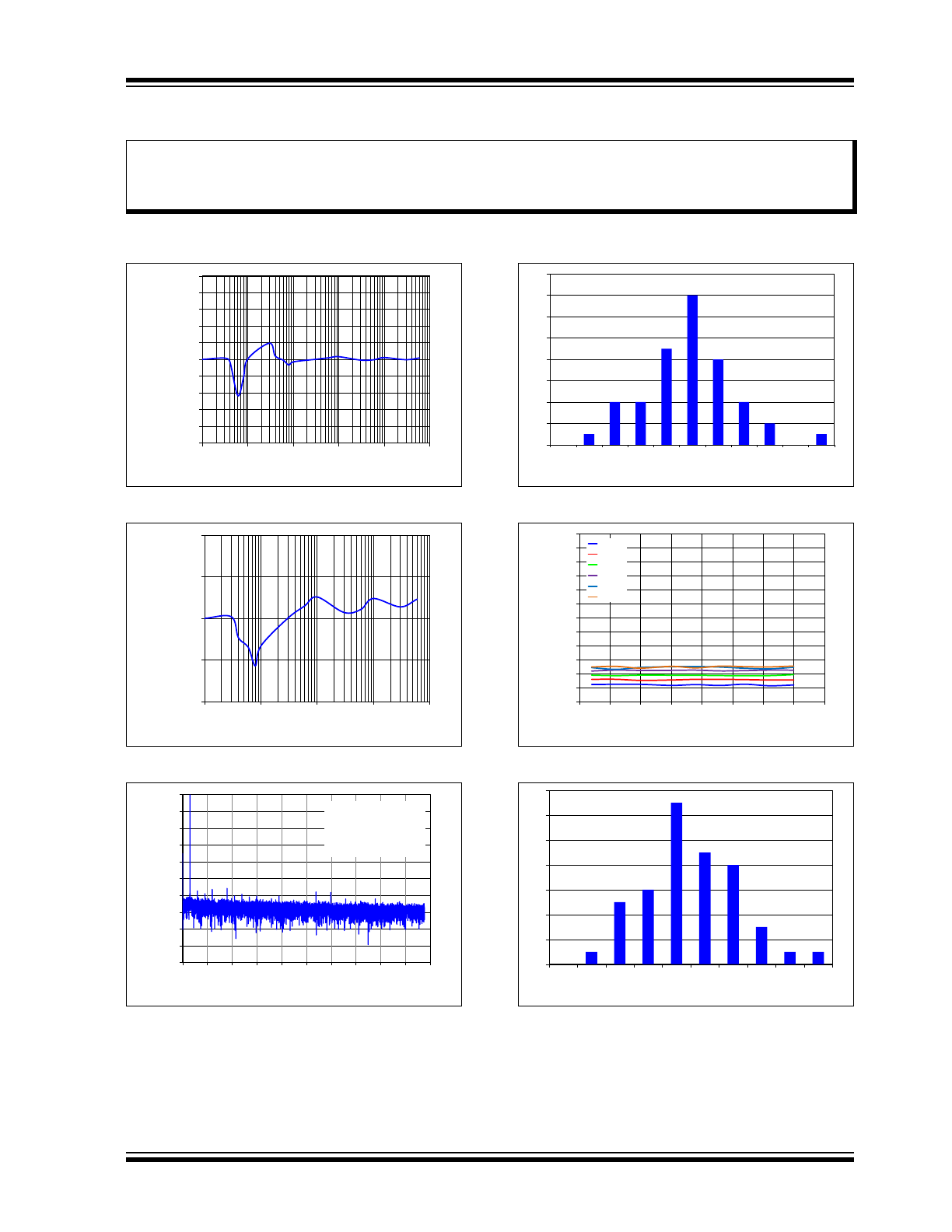
2.0
TYPICAL PERFORMANCE CURVES
Note: Unless otherwise indicated, AV
DD
= 3.3V, DV
DD
= 3.3V, T
A
= +25°C, GAIN = 1, V
IN
= -0.5 dBFS at 60 Hz
.
FIGURE 2-1:
Active Power, Gain = 1.
FIGURE 2-2:
RMS Current, Gain = 1.
FIGURE 2-3:
Spectral Response.
FIGURE 2-4:
THD Histogram.
FIGURE 2-5:
THD vs. Temperature.
FIGURE 2-6:
SNR Histogram.
Note:
The graphs and tables provided following this note are a statistical summary based on a limited number of
samples and are provided for informational purposes only. The performance characteristics listed herein
are not tested or guaranteed. In some graphs or tables, the data presented may be outside the specified
operating range (e.g., outside specified power supply range) and therefore outside the warranted range.
-0.50%
-0.40%
-0.30%
-0.20%
-0.10%
0.00%
0.10%
0.20%
0.30%
0.40%
0.50%
0.01
0.1
1
10
100
1000
Measurement Error (%
)
Current Channel Input Amplitude (mV
PEAK
)
-0.100%
-0.050%
0.000%
0.050%
0.100%
0.1
1
10
100
1000
RMS Current Error (%
)
Input Voltage RMS (mV
PP
)
-200
-180
-160
-140
-120
-100
-80
-60
-40
-20
0
0
200 400 600 800 1000 1200 1400 1600 1800 2000
Amplitude (dB)
Frequency (Hz)
f
IN
= -0.5 dBFS @ 60 Hz
f
D
= 3.9 ksps
16384 pt FFT
OSR = 256
Dithering = Maximum
-107.3 -107.1 -107.0 -106.8 -106.7 -106.5 -106.4 -106.2 -106.1 -105.9 -105.8
Frequency
of
Occurrence
Total Harmonic Distortion (-dBc)
-120
-110
-100
-90
-80
-70
-60
-50
-40
-30
-20
-10
0
-50
-25
0
25
50
75
100
125
150
T
o
tal Harominc
Distortion (dBc)
Temperature (°C)
G = 1
G = 2
G = 4
G = 8
G = 16
G = 32
94.2 94.3 94.5 94.6 94.8 94.9 95.1 95.2 95.4 95.5
Frequency
of
Occurrence
Signal-to-Noise and Distortion Ratio (dB)
MCP39F501
DS20005256A-page 8
2013 Microchip Technology Inc.
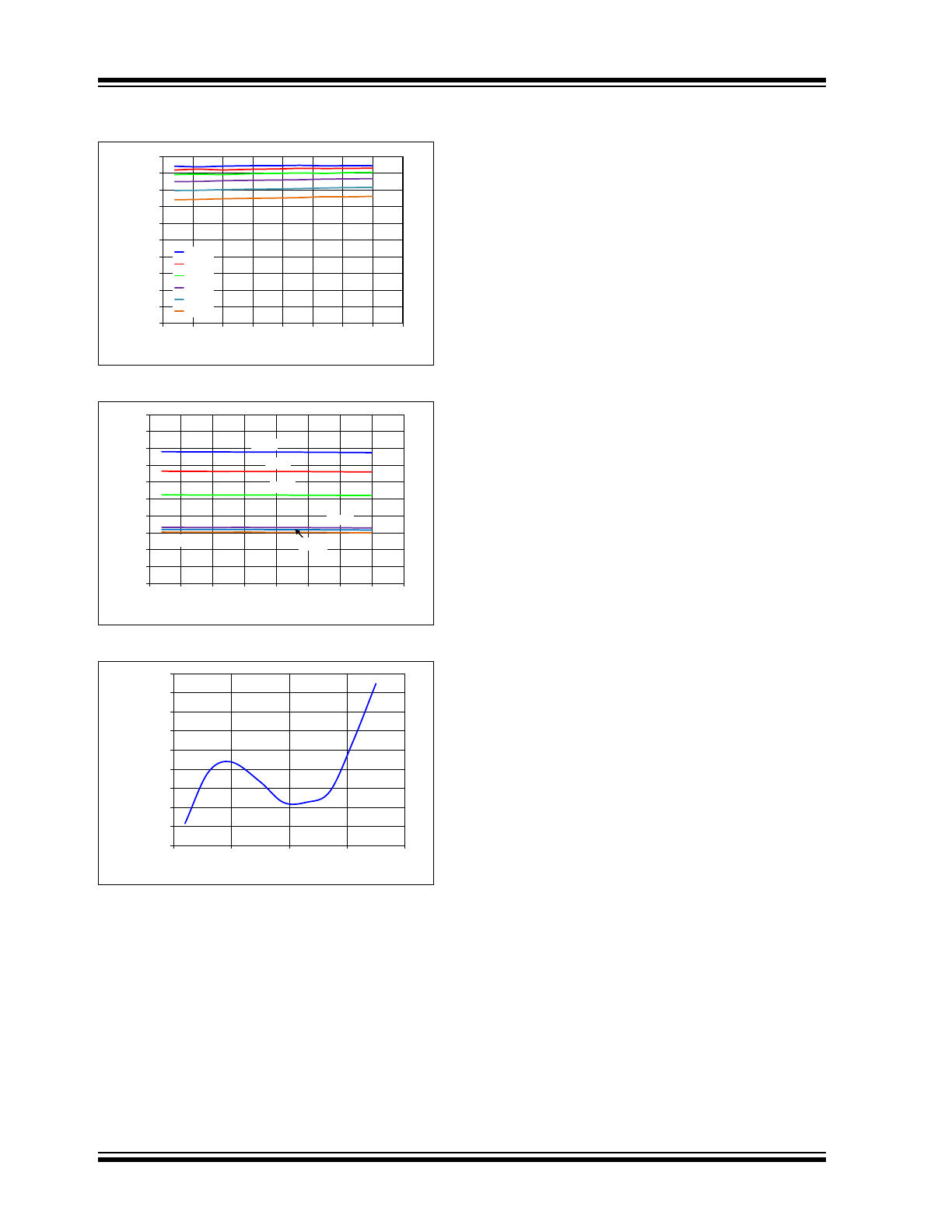
Note: Unless otherwise indicated, AV
DD
= 3.3V, DV
DD
= 3.3V, T
A
= +25°C, GAIN = 1, V
IN
= -0.5 dBFS at 60 Hz
.
FIGURE 2-7:
SINAD vs. Temperature.
FIGURE 2-8:
Gain Error vs. Temperature.
FIGURE 2-9:
Internal Voltage Reference
vs. Temperature.
0
10
20
30
40
50
60
70
80
90
100
-50
-25
0
25
50
75
100
125
150
Signal-to-Noise and
Distortion
Ration (dB)
Temperature (°C)
G = 1
G = 2
G = 4
G = 8
G = 16
G = 32
-5
-4
-3
-2
-1
0
1
2
3
4
5
-50
-25
0
25
50
75
100
125
150
Gain Error
(%
)
Temperature (°C)
G = 32
G = 16
G = 8
G = 4
G = 2
G = 1
1.1999
1.2000
1.2001
1.2002
1.2003
1.2004
1.2005
1.2006
1.2007
1.2008
-50
0
50
100
150
Internal V
o
ltage
Reference
(V)
Temperature (°C)
2013 Microchip Technology Inc.
DS20005256A-page 9
MCP39F501
3.0
PIN DESCRIPTION
The description of the pins are listed in
Table 3-1
.
TABLE 3-1:
PIN FUNCTION TABLE
MCP39F501
5x5 QFN
Symbol
Function
1
MODE/DIR
Single or Multiple Device mode with direction control for RS-485 drivers
2
NC
No Connect (must be left floating)
3
NC
No Connect (must be left floating)
4
UART_RX
UART Communication RX Pin
5
COMMON
A
Common pin A, to be connected to COMMON
B
6
OSCI
Oscillator Crystal Connection Pin or External Clock Input Pin
7
OSCO
Oscillator Crystal Connection Pin
8
NC
No Connect (must be left floating)
9
NC
No Connect (must be left floating)
10
RESET
Reset Pin for Delta Sigma ADCs
11
AV
DD
Analog Power Supply Pin
12
UART_TX
UART Communication TX Pin
13
COMMON
B
Common pin B, to be connected to COMMON
A
14
A0/DIO0
Address Select Pin 0 / Configurable digital I/O 0
15
A1/DIO1
Address Select Pin 1 / Configurable digital I/O 1
16
I1+
Non-Inverting Current Channel Input for 24-bit
ADC
17
I1-
Inverting Current Channel Input for 24-bit
ADC
18
V1-
Inverting Voltage Channel Input for 24-bit
ADC
19
V1+
Non-Inverting Voltage Channel Input for 24-bit
ADC
20
AN_IN/DIO2
Analog Input for SAR ADC / Configurable Digital Input/Output 2 Pin
21
A
GND
Analog Ground Pin, Return Path for internal analog circuitry
22
DIO3
Configurable Digital Input/Output 3
23
REFIN+/OUT
Non-Inverting Voltage Reference Input and Internal Reference Output Pin
24
D
GND
Digital Ground Pin, Return Path for internal digital circuitry
25
DV
DD
Power Supply Pin
26
MCLR
Master Clear for Device
27
D
GND
Digital Ground Pin, Return Path for internal digital circuitry
28
DR
Data Ready (must be left floating)
29
EP
Exposed Thermal Pad (to be connected to D
GND
)

MCP39F501
DS20005256A-page 10
2013 Microchip Technology Inc.
3.1
Single/Multiple Device Mode and
Direction Pin (MODE/DIR)
When using multiple devices on a single bus, this pin
should be tied to the DIR pin of the transceiver for
direction control. This will cause the A0/DIO0 and
A1/DIO1 pins to act as address pins A0,A1. If additional
devices are required, the Device Address register can
be programmed to allow for more than four devices.
For this operation, a 4.7 k
pull-down resistor should
be connected to this pin.
If only a single device is being used, the MODE pin
should be driven high at power-on reset (POR), making
the A0/DIO0 and A1/DIO1 pins additional configurable
digital I/O (DIO).
3.2
UART Communication Pins
(UART_TX, UART_RX)
The MCP39F501 device contains an asynchronous
full-duplex UART. The UART communication is 8 bits
with Start and Stop bit. See
Section 4.2 “UART
Settings”
for more information.
3.3
Common Pins (COMMON A and B)
The COMMON
A
and COMMON
B
pins are internal
connections for the MCP39F501. These two pins
should be connected together in the application.
3.4
Data Ready Pin (DR)
The data ready pin indicates if a new delta-sigma A/D
conversion result is ready to be processed. This pin is
for indication only and should be left floating. After each
conversion is finished, a low pulse will take place on the
Data Ready pin to indicate the conversion result is
ready and an interrupt is generated in the calculation
engine (CE). This pulse is synchronous with line
frequency and has a predefined and constant width.
3.5
Oscillator Pins (OSCO/OSCI)
OSCO and OSCI provide the master clock for the
device. Appropriate load capacitance should be
connected to these pins for proper operation. An
optional 4 MHz crystal can be connected to these pins.
If a crystal of external clock source is not detected, the
device will clock from the internal 4 MHz oscillator.
3.6
Reset Pin (RESET)
This pin is active-low and places the delta-sigma
ADCs, PGA, internal V
REF
and other blocks associated
with the analog front-end in a reset state when pulled
low. This input is Schmitt-triggered.
3.7
Analog Power Supply Pin (AV
DD
)
AV
DD
is the power supply pin for the analog circuitry
within the MCP39F501.
This pin requires appropriate bypass capacitors and
should be maintained to 2.7V and 3.6V for specified
operation. It is recommended to use 0.1 µF ceramic
capacitors.
3.8
Digital Power Supply Pin (DV
DD
)
DV
DD
is the power supply pin for the digital circuitry
within the MCP39F501. This pin requires appropriate
bypass capacitors and should be maintained between
2.7V and 3.6V for specified operation. It is
recommended to use 0.1 µF ceramic capacitors.
3.9
Configurable Digital Input/Output
Pins (DIOn)
These digital I/O pins can be configured to act as input
or as output events, such as alarm events or interrupt
flags, based on the device configuration. For more
information, see
Section 8.0 “Configurable Digital
I/O Pins (DIO Configuration – 0x0046)”
.
3.10
24-Bit Delta Sigma ADC
Differential Current Channel
Input Pins (I1+/I1-)
I1- and I1+ are the two fully-differential current channel
inputs for the Delta-Sigma ADCs.
The linear and specified region of the channels are
dependent on the PGA gain. This region corresponds
to a differential voltage range of ±600 mV
PEAK
/GAIN
with V
REF
= 1.2V.
The maximum absolute voltage, with respect to A
GND
,
for each In+/- input pin is ±1V with no distortion and
±6V with no breaking after continuous voltage.
3.11
24-Bit Delta Sigma ADC
Differential Voltage Channel
Inputs (V1+/V1-)
V1- and V1+ are the two fully-differential voltage
channel inputs for the Delta-Sigma ADCs.
The linear and specified region of the channels are
dependent on the PGA gain. This region corresponds
to a differential voltage range of ±600 mV
PEAK
/GAIN
with V
REF
= 1.2V.
The maximum absolute voltage, with respect to A
GND
,
for each V
N
+/- input pin is ±1V with no distortion and
±6V, with no breaking after continuous voltage.
Note:
This pin is internally connected to the IRQ
of the calculation engine and should be
left floating.