
2006-2012 Microchip Technology Inc.
DS22025C-page 1
MCP3909
Features
• Supports IEC 62053 International Energy
Metering Specification
• Digital Waveform Data Access Through SPI
Interface
- 16-bit Dual ADC Output Data Words
- 20-bit Multiplier Output Data Word
• Dual Functionality Pins Support Serial Interface
Access and Simultaneous Active Power Pulse
Output
• Two 16-bit Second Order Delta-sigma Analog-
to-Digital Converters (ADCs) with Multi-bit DAC
- 81 dB SINAD (typical) on Both Channels
• 0.1% Typical Active Energy Measurement Error
Over 1000:1 Dynamic Range
• PGA for Small Signal Input Supports Low Value
Shunt Current Sensor
• Ultra-low Drift On-chip Reference,15 ppm/°C
(typical)
• Direct Drive for Electromagnetic Mechanical
Counter and Two-phase Stepper Motors
• Low I
DD
of 4 mA (maximum)
• Tamper Output Pin for Negative Power Indication
• Temperature Ranges:
- Industrial: -40°C to +85°C
- Extended: -40°C to +125°C
Description
The MCP3909 device is an energy-metering IC
designed to support the IEC 62053 international meter-
ing standard specification. It supplies a frequency out-
put proportional to the average active real power, with
simultaneous serial access to ADC channels and mul-
tiplier output data. This output waveform data is avail-
able at up to 14 kHz with 16-bit ADC output and 20-bit
multiplier output words. The 16-bit, delta-sigma ADCs
allow for a wide range of I
B
and I
MAX
currents and/or
small shunt (<200 µOhms) meter designs. A no-load
threshold block prevents any current creep measure-
ments for the active power pulse outputs.
The integrated on-chip voltage reference has an
ultra-low temperature drift of 15 ppm per degree C.
This accurate energy metering IC with high field reli-
ability is available in the industry standard 24-lead
SSOP pinout.
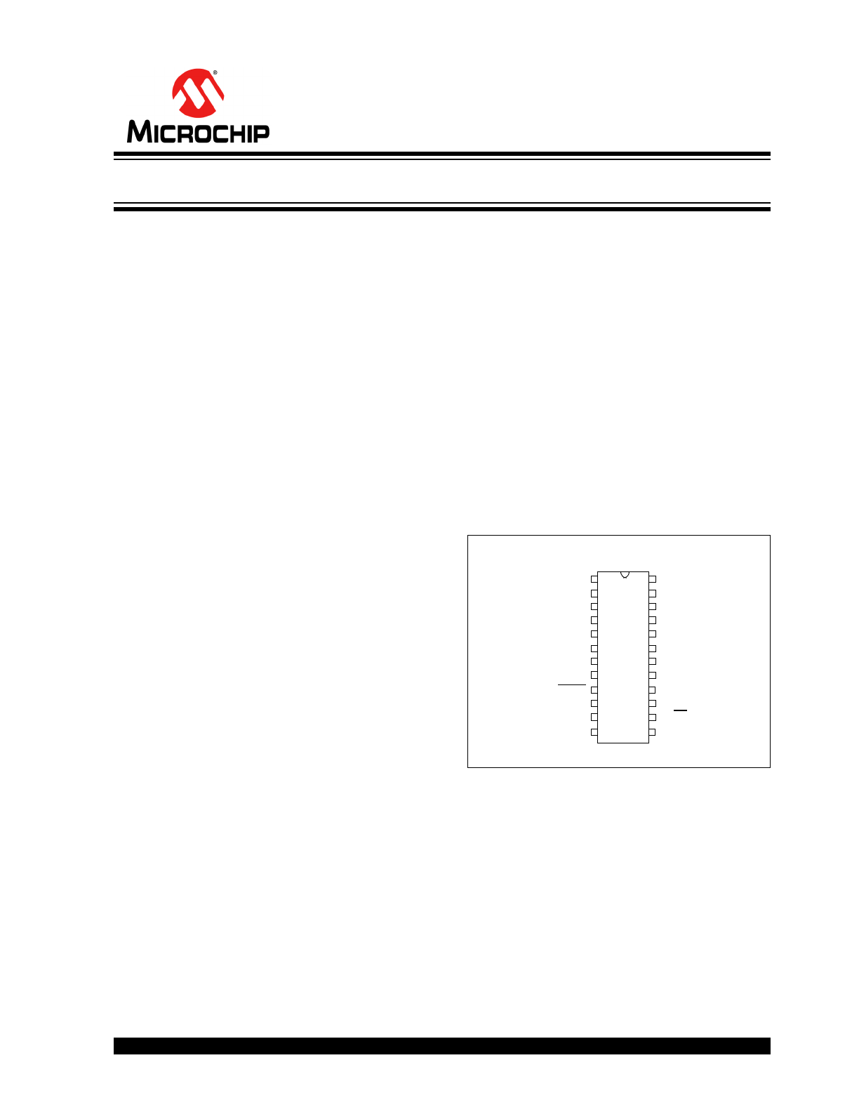
Package Type
F
OUT0
D
GND
NEG/SDO
1
2
3
4
24
23
22
21
20
19
18
17
5
6
7
8
F
OUT1
NC
CLKOUT
CLKIN
DV
DD
HPF
AV
DD
NC
CH0+
CH0-
CH1-
CH1+
HF
OUT
16
9
G0
MCLR
15
14
10
11
G1
F0/CS
REFIN/OUT
A
GND
13
12
F1/SDI
F2/SCK
24-Lead
SSOP
Energy Metering IC with SPI Interface and Active Power Pulse Output
MCP3909
DS22025C-page 2
2006-2012 Microchip Technology Inc.
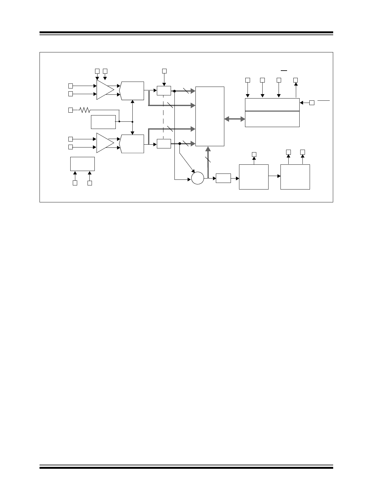
Functional Block Diagram
16-bit
ADC
+
–
CH0+
CH0-
Reference
2.4V
+
–
CH1+
CH1-
HPF1
LPF1
DTF
conversion
REFIN/OUT
F
OUT1
HF
OUT
G0 G1
F2/SCK F1/SDI
F
OUT0
OSC1 OSC2
NEG/SDO
HPF
F0/CS
Multi-level
16-bit
ADC
Multi-level
X
PGA
Serial Control
Buffers
And Output
Stepper Motor
Output Drive
Active Power
SPI
Interface
Dual Functionality Pin
Control
20
16
16
16
16
MCLR
Sub-system
Clock
for
Active Power
HPF1
4 k
2006-2012 Microchip Technology Inc.
DS22025C-page 3
MCP3909
1.0
ELECTRICAL
CHARACTERISTICS
Absolute Maximum Ratings †
V
DD
...................................................................................7.0V
Digital inputs and outputs w.r.t. A
GND
....... -0.6V to V
DD
+0.6V
Analog input w.r.t. A
GND
..................................... ....-6V to +6V
V
REF
input w.r.t. A
GND
.............................. -0.6V to V
DD
+0.6V
Storage temperature .....................................-65°C to +150°C
Ambient temp. with power applied ................-65°C to +125°C
Soldering temperature of leads (10 seconds) ............. +300°C
ESD on the analog inputs (HBM,MM) ................. 5.0 kV, 500V
ESD on all other pins (HBM,MM) ........................5.0 kV, 500V
† Notice: Stresses above those listed under "Maximum Rat-
ings" may cause permanent damage to the device. This is a
stress rating only and functional operation of the device at
those or any other conditions above those indicated in the
operation listings of this specification is not implied. Exposure
to maximum rating conditions for extended periods may affect
device reliability.
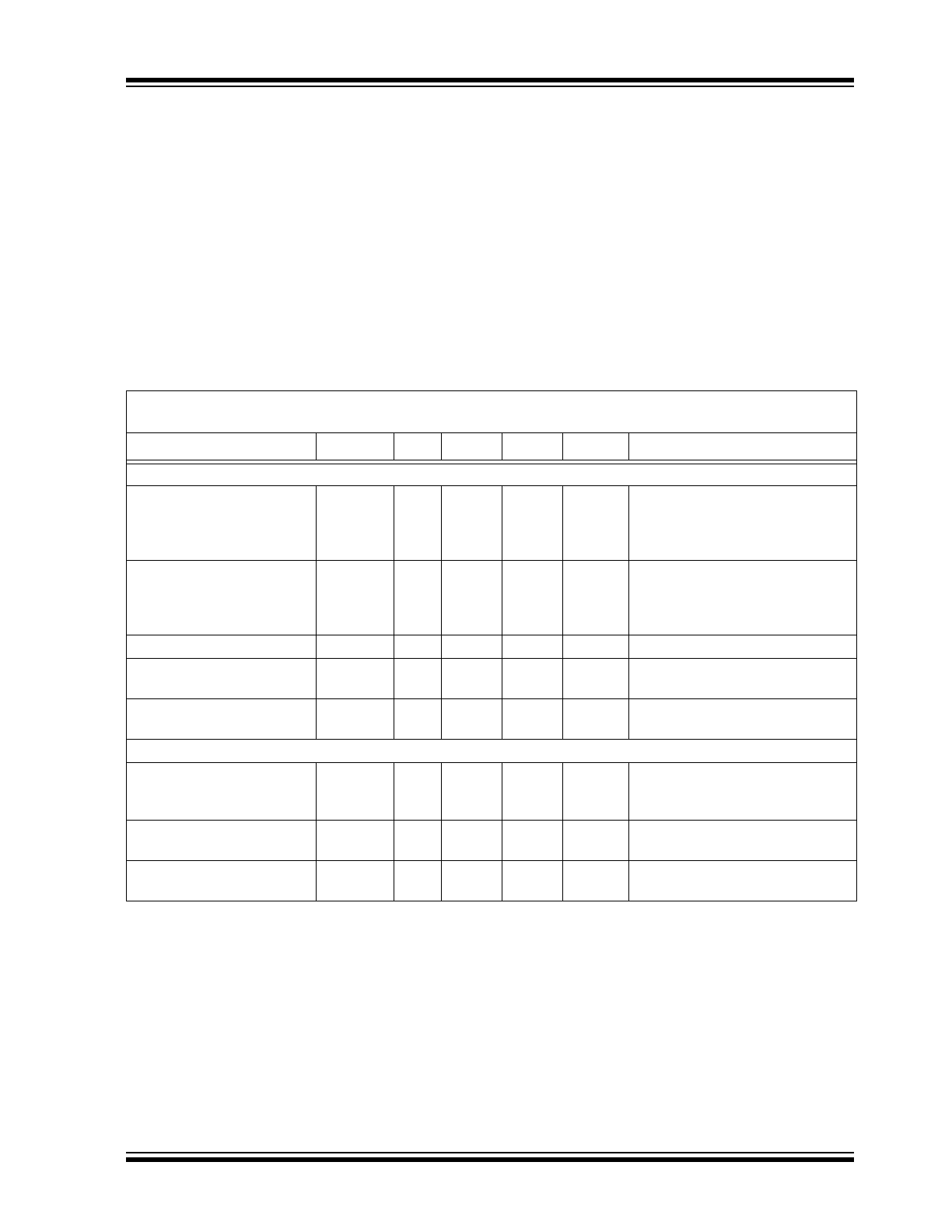
ELECTRICAL CHARACTERISTICS
Electrical Specifications: Unless otherwise indicated, all parameters apply at AV
DD
= DV
DD
= 4.5V to 5.5V,
Internal V
REF
, HPF turned on (AC mode), A
GND
, D
GND
= 0V, MCLK = 3.58 MHz; T
A
= -40°C to +85°C.
Parameter
Sym
Min
Typ.
Max
Units
Comment
Active Power Measurement Accuracy
Active Energy Measurement
Error
E
—
0.1
—
% F
OUT
Channel 0 swings 1000:1 range,
F
OUT0
, F
OUT1
Frequency outputs
only, does not apply to serial
interface data. (
Note 1
,
Note 4
)
No-Load Threshold/
Minimum Load
NLT
—
0.0015
—
% F
OUT
Max
Frequency outputs only, does not
apply to serial interface data.
Disabled when F2, F1, F0 = 0, 1, 1
(
Note 5
,
Note 6
)
System Gain Error
—
1
5
% F
OUT
(
Note 2
,
Note 5
)
AC Power Supply Rejection
(output frequency variation)
AC PSRR
—
0.01
—
% F
OUT
F2, F1, F0 = 0, 1, 1 (
Note 3
)
DC Power Supply Rejection
(output frequency variation)
DC PSRR
—
0.01
—
% F
OUT
HPF = 1, Gain = 1 (
Note 3
)
Waveform Sampling
A/D Converter Signal-to-
Noise and Distortion Ratio
SINAD
—
81
—
dB
Applies to both channels,
V
IN
= 0 dBFS at 50 Hz
(V
IN
= Full Scale)
Bandwidth
(Notch Frequency)
—
14
—
kHz
Applies to both channels,
MCLK/256
Phase Delay Between
Channels
—
—
1/MCLK
s
HPF = 0 and 1, < 1 MCLK period
(
Note 4
,
Note 6
,
Note 7
)
Note 1:
Measurement error = (Energy Measured By Device - True Energy)/True Energy * 100%. Accuracy is mea-
sured with signal (±660 mV) on Channel 1. F
OUT0
, F
OUT1
pulse outputs. Valid from 45 Hz to 75 Hz. See
typical performance curves for higher frequencies and increased dynamic range. This parameter is not
100% production tested.
2:
Does not include internal V
REF
. Gain = 1, CH0 = 470 mVDC, CH1 = 660 mVDC, difference between
measured output frequency and expected transfer function.
3:
Percent of HF
OUT
output frequency variation; Includes external V
REF
= 2.5V, CH1 = 100 mV
RMS
@ 50 Hz,
CH2 = 100 mV
RMS
@ 50 Hz, AV
DD
= 5V + 1 V
pp
@ 100 Hz. DC PSRR: 5V ±500 mV
4:
Error applies down to 60 degree lead (PF = 0.5 capacitive) and 60 degree lag (PF = 0.5 inductive).
5:
Refer to Section 4.0 “Device Overview” for complete description.
6:
Specified by characterization, not production tested.
7:
1 MCLK period at 3.58 MHz is equivalent to less than < 0.005 degrees at 50 or 60 Hz.
MCP3909
DS22025C-page 4
2006-2012 Microchip Technology Inc.
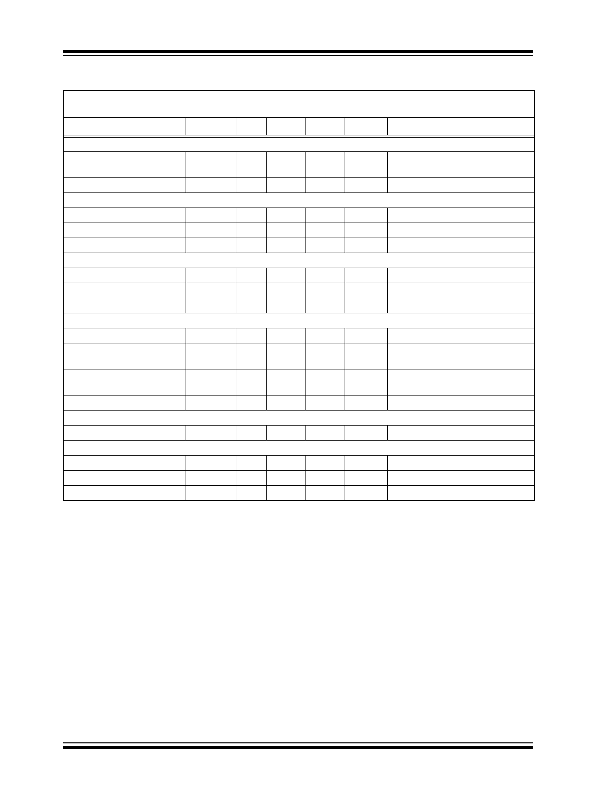
ADC/PGA Specifications
Offset Error
V
OS
—
2
5
mV
Referred to Input, applies to both
channels
Gain Error Match
—
0.5
—
% F
OUT
(
Note 5
)
Internal Voltage Reference
Voltage
—
2.4
—
V
Tolerance
—
±2
—
%
Tempco
—
15
—
ppm/°C
Reference Input
Input Range
2.2
—
2.6
V
Input Impedance
3.2
—
—
kΩ
Input Capacitance
—
—
10
pF
Analog Inputs
Maximum Signal Level
—
—
±1
V
CH0+,CH0-,CH1+,CH1- to A
GND
Differential Input Voltage
Range Channel 0
—
—
±470/G
mV
G = PGA Gain on Channel 0
Differential Input Voltage
Range Channel 1
—
—
±660
mV
Input Impedance
390
—
—
kΩ
Proportional to 1/MCLK
Oscillator Input
Frequency Range
MCLK
1
—
4
MHz
Power Specifications
Operating Voltage
4.5
—
5.5
V
AV
DD,
DV
DD
I
DD,A
I
DD,A
—
2.3
2.8
mA
AV
DD
pin only
I
DD,D
I
DD,D
—
0.8
1.2
mA
DV
DD
pin only
ELECTRICAL CHARACTERISTICS (CONTINUED)
Electrical Specifications: Unless otherwise indicated, all parameters apply at AV
DD
= DV
DD
= 4.5V to 5.5V,
Internal V
REF
, HPF turned on (AC mode), A
GND
, D
GND
= 0V, MCLK = 3.58 MHz; T
A
= -40°C to +85°C.
Parameter
Sym
Min
Typ.
Max
Units
Comment
Note 1:
Measurement error = (Energy Measured By Device - True Energy)/True Energy * 100%. Accuracy is mea-
sured with signal (±660 mV) on Channel 1. F
OUT0
, F
OUT1
pulse outputs. Valid from 45 Hz to 75 Hz. See
typical performance curves for higher frequencies and increased dynamic range. This parameter is not
100% production tested.
2:
Does not include internal V
REF
. Gain = 1, CH0 = 470 mVDC, CH1 = 660 mVDC, difference between
measured output frequency and expected transfer function.
3:
Percent of HF
OUT
output frequency variation; Includes external V
REF
= 2.5V, CH1 = 100 mV
RMS
@ 50 Hz,
CH2 = 100 mV
RMS
@ 50 Hz, AV
DD
= 5V + 1 V
pp
@ 100 Hz. DC PSRR: 5V ±500 mV
4:
Error applies down to 60 degree lead (PF = 0.5 capacitive) and 60 degree lag (PF = 0.5 inductive).
5:
Refer to Section 4.0 “Device Overview” for complete description.
6:
Specified by characterization, not production tested.
7:
1 MCLK period at 3.58 MHz is equivalent to less than < 0.005 degrees at 50 or 60 Hz.
2006-2012 Microchip Technology Inc.
DS22025C-page 5
MCP3909
TEMPERATURE CHARACTERISTICS
Electrical Specifications: Unless otherwise indicated, V
DD
= 4.5V to 5.5V, A
GND
, D
GND
= 0V.
Parameters
Sym
Min
Typ
Max
Units
Conditions
Temperature Ranges
Specified Temperature Range
T
A
-40
—
+85
°C
Operating Temperature Range
T
A
-40
—
+125
°C
Note
Storage Temperature Range
T
A
-65
—
+150
°C
Thermal Package Resistances
Thermal Resistance, 24L-SSOP
JA
—
73
—
°C/W
Note:
The MCP3909 operates over this extended temperature range, but with reduced performance. In any case,
the Junction Temperature (T
J
) must not exceed the Absolute Maximum specification of +150°C.
TIMING CHARACTERISTICS
Electrical Specifications: Unless otherwise indicated, all parameters apply at AV
DD
= DV
DD
= 4.5V to 5.5V,
A
GND
, D
GND
= 0V, MCLK = 3.58 MHz; T
A
= -40°C to +85°C.
Parameter
Sym
Min
Typ
Max
Units
Comment
Frequency Outputs
F
OUT0
and F
OUT1
Pulse Width
(Logic Low)
t
FW
—
275
—
ms
984376 MCLK periods
(
Note 1
)
HF
OUT
Pulse Width
t
HW
—
90
—
ms
322160 MCLK periods
(
Note 2
)
F
OUT0
and F
OUT1
Pulse Period
t
FP
Refer to
Equation 4-1
s
HF
OUT
Pulse Period
t
HP
Refer to
Equation 4-2
s
F
OUT0
to F
OUT1
Falling-Edge
Time
t
FS2
—
0.5 t
FP
—
F
OUT0
to F
OUT1
Minimum Sepa-
ration
t
FS
—
4/MCLK
—
Digital I/O
F
OUT0
and F
OUT1
Output High
Voltage
V
OH
4.5
—
—
V
I
OH
= 10 mA, DV
DD
= 5.0V
F
OUT0
and F
OUT1
Output Low
Voltage
V
OL
—
—
0.5
V
I
OL
= 10 mA, DV
DD
= 5.0V
HF
OUT
and NEG Output High
Voltage
V
OH
4.0
—
—
V
I
OH
= 5 mA, DV
DD
= 5.0V
HF
OUT
and NEG Output Low
Voltage
V
OL
—
—
0.5
V
I
OL
= 5 mA, DV
DD
= 5.0V
High-Level Input Voltage
(All Digital Input Pins)
V
IH
2.4
—
—
V
DV
DD
= 5.0V
Low Level Input Voltage
(All Digital Input Pins)
V
IL
—
—
0.85
V
DV
DD
= 5.0V
Input Leakage Current
—
0.1
±1
µA
V
IN
= 0, V
IN
= DV
DD
Pin Capacitance
—
—
10
pF
(
Note 3
)
Note 1:
If output pulse period (t
FP
) falls below 984376*2 MCLK periods, then t
FW
= 1/2 t
FP
.
2:
If output pulse period (t
HP
) falls below 322160*2 MCLK periods, then t
HW
= 1/2 t
HP
. When F2, F1, F0
equals 0,1,1, the HF
OUT
pulse time is fixed at 64 x MCLK periods or 18 µs for MCLK = 3.58 MHz.
3:
Specified by characterization, not production tested.
4:
Serial timings specified and production tested with 180 pF load.
MCP3909
DS22025C-page 6
2006-2012 Microchip Technology Inc.
Serial Interface Timings (
Note 4
)
Data Ready Pulse Width
t
DR
4/MCLK
Reset Time
t
RST
100
—
—
ns
Output Data Rate
f
ADC
—
MCLK/256
—
Serial Clock Frequency
f
CLK
—
20
MHz
V
DD
= 5V
Window for serial mode entry
codes
t
WINDOW
—
—
32/
MCLK
—
Last bit must be clocked in
before this time.
Window start time for serial
mode entry codes
t
WINSET
1/MCLK
—
—
—
First bit must be clocked in
after this time.
Serial Clock High Time
t
HI
—
—
25
ns
f
CLK
= 20 MHz
Serial Clock Low Time
t
LO
—
—
25
ns
f
CLK
= 20 MHz
CS Fall to First Rising CLK Edge
t
SUCS
15
—
—
ns
Data Input Setup Time
t
SU
10
—
—
ns
Data Input Hold Time
t
HD
—
—
10
ns
CS Rise to Output Disable
t
DIS
—
—
150
ns
CLK Rise to Output Data Valid
t
DO
—
—
30
ns
SDO Rise Time
t
R
—
2
—
ns
SDO Fall Time
t
F
—
2
—
ns
TIMING CHARACTERISTICS (CONTINUED)
Electrical Specifications: Unless otherwise indicated, all parameters apply at AV
DD
= DV
DD
= 4.5V to 5.5V,
A
GND
, D
GND
= 0V, MCLK = 3.58 MHz; T
A
= -40°C to +85°C.
Parameter
Sym
Min
Typ
Max
Units
Comment
Note 1:
If output pulse period (t
FP
) falls below 984376*2 MCLK periods, then t
FW
= 1/2 t
FP
.
2:
If output pulse period (t
HP
) falls below 322160*2 MCLK periods, then t
HW
= 1/2 t
HP
. When F2, F1, F0
equals 0,1,1, the HF
OUT
pulse time is fixed at 64 x MCLK periods or 18 µs for MCLK = 3.58 MHz.
3:
Specified by characterization, not production tested.
4:
Serial timings specified and production tested with 180 pF load.
2006-2012 Microchip Technology Inc.
DS22025C-page 7
MCP3909
FIGURE 1-1:
Output Timings for Active Power Pulse Outputs and Negative Power Pin.
FIGURE 1-2:
Serial Interface Timings showing Output, Rise, Hold, and CS Times.
F
OUT0
t
FP
F
OUT1
HF
OUT
t
FW
t
HP
t
HW
t
FS
t
FS2
NEG
CS
CLK
SDI
t
SU
t
HD
t
SUCS
t
HI
t
LO
SDO
t
DO
t
R
t
F
t
DIS
t
CLK
Hi-z
MCP3909
DS22025C-page 8
2006-2012 Microchip Technology Inc.
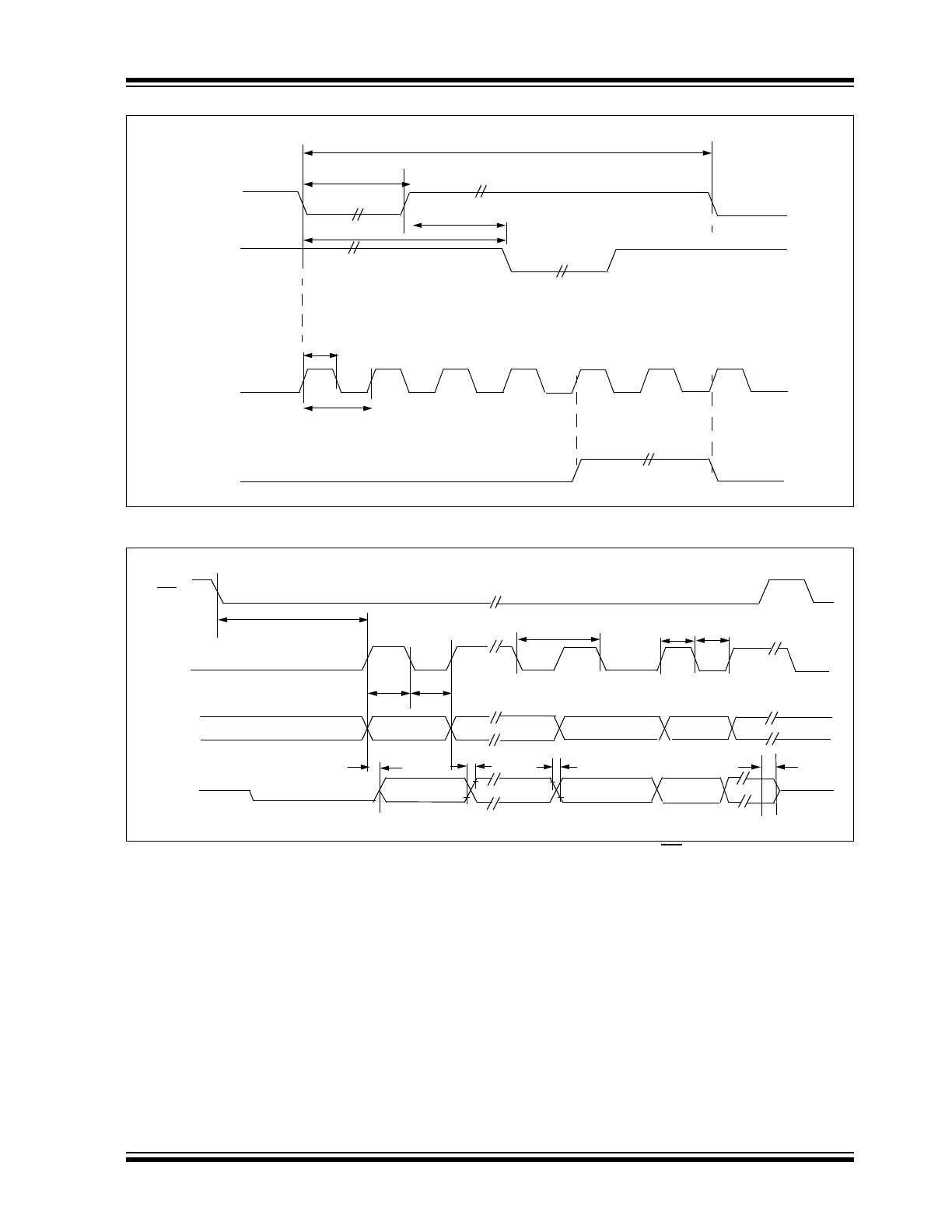
FIGURE 1-3:
SPI Output Pin Loading Circuit During SPI Testing.
SPI Data
Output
Pin
V
DD
180 pF
R
VDD VOL
–
IOL
------------------------------------
=
R
VOH
IOH
------------------
=
2006-2012 Microchip Technology Inc.
DS22025C-page 9
MCP3909
2.0
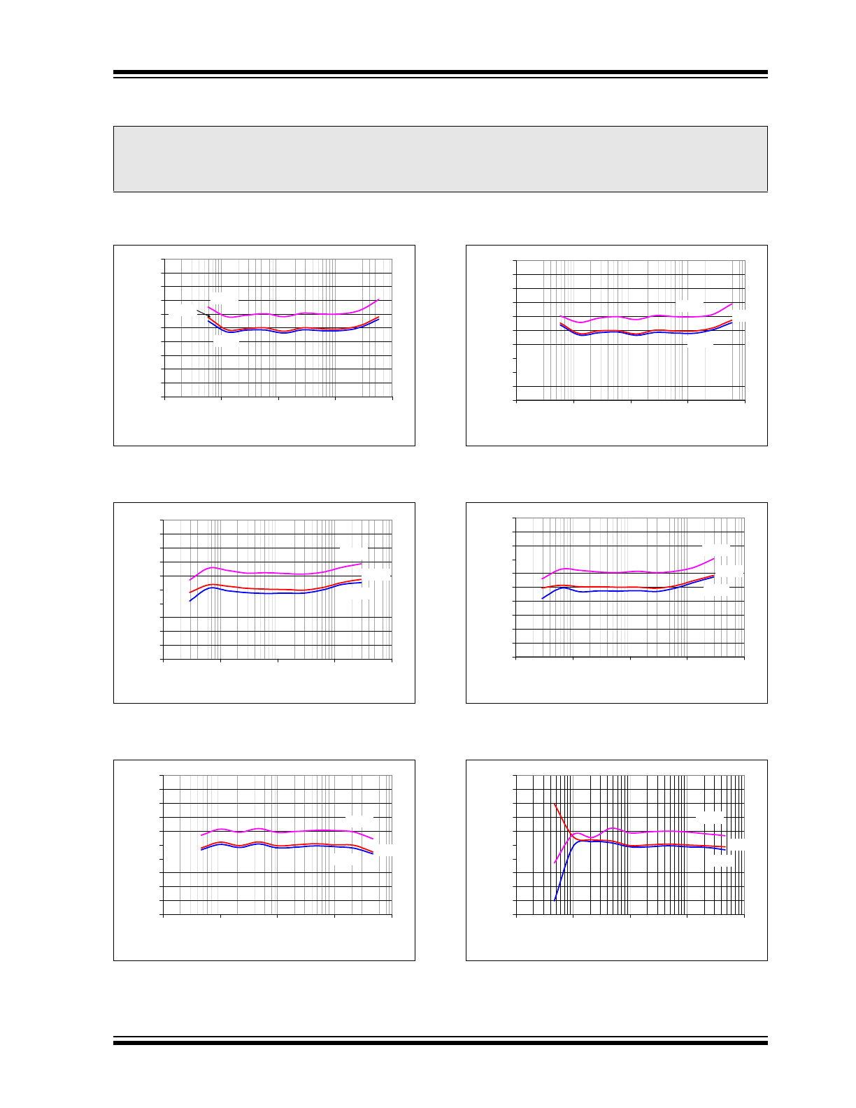
TYPICAL PERFORMANCE CURVES
Note: Unless otherwise specified, DV
DD
, AV
DD
= 5V; A
GND
, D
GND
= 0V; V
REF
= Internal, HPF = 1 (AC mode),
MCLK = 3.58 MHz, CH1 input = 660 mV
P-P
at 50 Hz, CH0 amplitude sweeps at 50 Hz.
FIGURE 2-1:
Active Power Measurement
Error (Gain = 8, PF = 1).
FIGURE 2-2:
Active Power Measurement
Error (Gain = 16, PF = 1).
FIGURE 2-3:
Active Power Measurement
Error (Gain = 2, PF = 1).
FIGURE 2-4:
Active Power Measurement
Error (Gain = 8, PF = 0.5).
FIGURE 2-5:
Active Power Measurement
Error (Gain = 16, PF = 0.5).
FIGURE 2-6:
Active Power Measurement
Error (Gain =2, PF = 0.5).
Note:
The graphs and tables provided following this note are a statistical summary based on a limited number of
samples and are provided for informational purposes only. The performance characteristics listed herein
are not tested or guaranteed. In some graphs or tables, the data presented may be outside the specified
operating range (e.g., outside specified power supply range) and therefore outside the warranted range.
-1
-0.8
-0.6
-0.4
-0.2
0
0.2
0.4
0.6
0.8
1
0.0000
0.0001
0.0010
0.0100
0.1000
CH0 Vp-p Amplitude (V)
Meas
u
remen
t E
rro
r (
%
)
+85°C
+25°C
-40°C
`
-1
-0.8
-0.6
-0.4
-0.2
0
0.2
0.4
0.6
0.8
1
0.0000
0.0001
0.0010
0.0100
0.1000
CH0 Vp-p Amplitude (V)
M
ea
su
rem
en
t E
rr
o
r (
%
)
+85°C
+25°C
- 40°C
-1
-0.8
-0.6
-0.4
-0.2
0
0.2
0.4
0.6
0.8
1
0.0001
0.0010
0.0100
0.1000
1.0000
CH0 Vp-p Amplitude (V)
M
e
as
ur
em
ent
E
rror
(
%
)
+85°C
+25°C
- 40°C
-1
-0.8
-0.6
-0.4
-0.2
0
0.2
0.4
0.6
0.8
1
0.0000
0.0001
0.0010
0.0100
0.1000
CH0 Vp-p Amplitude (V)
M
ea
su
rem
en
t E
rro
r
(%
)
+85°C
+25°C
-40°C
-1
-0.8
-0.6
-0.4
-0.2
0
0.2
0.4
0.6
0.8
1
0.0000
0.0001
0.0010
0.0100
0.1000
CH0 Vp-p Amplitude (V)
M
ea
su
rem
en
t E
rr
o
r (
%
)
+85°C
+25°C
-40°C
-1
-0.8
-0.6
-0.4
-0.2
0
0.2
0.4
0.6
0.8
1
0.0001
0.0010
0.0100
0.1000
1.0000
CH0 Vp-p Amplitude (V)
M
e
as
ur
em
ent
E
rror
(
%
)
+85°C
+25°C
-40°C
MCP3909
DS22025C-page 10
2006-2012 Microchip Technology Inc.
Note: Unless otherwise specified, DV
DD
, AV
DD
= 5V; A
GND
, D
GND
= 0V; V
REF
= Internal, HPF = 1 (AC mode),
MCLK = 3.58 MHz, CH1 input = 660 mV
P-P
at 50 Hz, CH0 amplitude sweeps at 50 Hz.
FIGURE 2-7:
Active Power Measurement
Error (Gain = 1, PF = 1).
L
FIGURE 2-8:
Active Power Measurement
Error (Gain = 1, PF = 0.5).
FIGURE 2-9:
Measurement Error,
Temperature = +125°C, Gain = 1.
FIGURE 2-10:
Measurement Error,
Temperature = +125°C, Gain = 2.
FIGURE 2-11:
Measurement Error,
Temperature = +125°C, Gain = 8.
FIGURE 2-12:
Measurement Error,
Temperature = +125°C, Gain = 16.
-1
-0.8
-0.6
-0.4
-0.2
0
0.2
0.4
0.6
0.8
1
0.0001
0.0010
0.0100
0.1000
1.0000
CH0 Vp-p Amplitude (V)
M
e
as
ur
em
ent
E
rror
(
%
)
+85°C
+25°C
- 40°C
-1
-0.8
-0.6
-0.4
-0.2
0
0.2
0.4
0.6
0.8
1
0.0001
0.0010
0.0100
0.1000
1.0000
CH0 Vp-p Amplitude (V)
M
e
as
ur
em
en
t E
rr
o
r
(%
)
+85°C
+25°C
-40°C
-1
-0.8
-0.6
-0.4
-0.2
0
0.2
0.4
0.6
0.8
1
0.0001
0.001
0.01
0.1
1
CH1 V
A
lit d (V)
Measurement Error (%)
+25°C; PF = 1
+25°C; PF = 0.5
+125°C; PF = 0.5
+125°C; PF = 1
-1
-0.8
-0.6
-0.4
-0.2
0
0.2
0.4
0.6
0.8
1
0.0001
0.001
0.01
0.1
1
CH1 Vp-p Amplitude (V)
Measurement Error (%)
+25°C; PF = 1
+25°C; PF = 0.5
+125°C; PF = 1
+125°C; PF = 0.5
-1
-0.8
-0.6
-0.4
-0.2
0
0.2
0.4
0.6
0.8
1
0.0001
0.001
0.01
0.1
1
CH1 Vp-p Amplitude (V)
Measurement Error (%)
+125°C; PF = 1
+125°C; PF = 0.5
+25°C; PF = 1
+25°C; PF = 0.5
-1
-0.8
-0.6
-0.4
-0.2
0
0.2
0.4
0.6
0.8
1
0.0001
0.001
0.01
0.1
1
CH1 Vp-p Amplitude (V)
Measurement Error (%)
+25°C; PF = 1
+25°C; PF = 0.5
+125°C; PF = 1
+125°C; PF = 0.5