
2005-2014 Microchip Technology Inc.
DS20001950F-page 1
MCP3550/1/3
Features:
• 22-Bit ADC in Small 8-pin MSOP Package with
Automatic Internal Offset and Gain Calibration
• Low-Output Noise of 2.5 µV
RMS
with Effective
Resolution of 21.9 Bits (MCP3550/1)
• 3 µV Typical Offset Error
• 2 ppm Typical Full Scale Error
• 6 ppm Maximum INL Error
• Total Unadjusted Error Less Than 10 ppm
• No Digital Filter Settling Time, Single-Command
Conversions through 3-wire SPI Interface
• Ultra-Low Conversion Current (MCP3550/1):
- 100 µA Typical (V
DD
= 2.7V)
- 120 µA Typical (V
DD
= 5.0V)
• Differential Input with V
SS
to V
DD
Common Mode
Range
• 2.7V to 5.5V Single-Supply Operation
• Extended Temperature Range:
- -40°C to +125°C
Applications:
• Weigh Scales
• Direct Temperature Measurement
• 6-digit DVMs
• Instrumentation
• Data Acquisition
• Strain Gauge Measurement
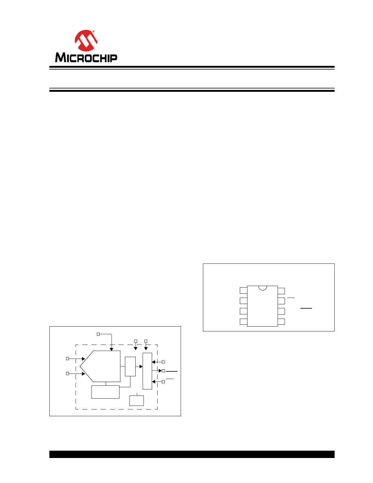
Block Diagram
Description:
The Microchip Technology Inc. MCP3550/1/3 devices
are 2.7V to 5.5V low-power, 22-bit Delta-Sigma
Analog-to-Digital Converters
ADCs). The devices offer
output noise as low as 2.5 µV
RMS
, with a total
unadjusted error of 10 ppm. The family exhibits 6 ppm
Integral Non-Linearity (INL) error, 3 µV offset error and
less than 2 ppm full scale error. The MCP3550/1/3
devices provide high accuracy and low noise
performance for applications where sensor
measurements (such as pressure, temperature and
humidity) are performed. With the internal oscillator
and high oversampling rate, minimal external
components are required for high-accuracy
applications.
This product line has fully differential analog inputs,
making it compatible with a wide variety of sensor,
industrial control or process control applications.
The MCP3550/1/3 devices operate from -40°C to
+125°C and are available in the space-saving 8-pin
MSOP and SOIC packages.
Package Types
V
SS
V
IN
+
V
IN
-
SCK
V
DD
SDO
CS
SINC
4
Internal
S
e
ri
a
l In
te
rf
a
ce
V
REF
POR
Oscillator
3rd-Order
DS ADC
Modulator
w/ Internal
Calibration
V
DD
RDY
V
IN
–
V
IN
+
MCP3550/1/3
V
SS
CS
SDO/RDY
1
2
3
4
8
7
6
5 SCK
V
DD
V
REF
MSOP, SOIC
Low-Power, Single-Channel 22-Bit Delta-Sigma ADCs

MCP3550/1/3
DS20001950F-page 2
2005-2014 Microchip Technology Inc.
NOTES:
2005-2014 Microchip Technology Inc.
DS20001950F-page 3
MCP3550/1/3
1.0
ELECTRICAL
CHARACTERISTICS
Absolute Maximum Ratings †
V
DD
...................................................................................7.0V
All inputs and outputs w.r.t V
SS
.... .......... -0.3V to V
DD
+ 0.3V
Difference Input Voltage ....................................... |V
DD
- V
SS
|
Output Short Circuit Current ................................ Continuous
Current at Input Pins ....................................................±2 mA
Current at Output and Supply Pins ............................±10 mA
Storage Temperature ....................................-65°C to +150°C
Ambient temp. with power applied ................-55°C to +125°C
ESD protection on all pins (HBM, MM)
6 kV, 400V
Maximum Junction Temperature (T
J
). .........................+150°C
†
Notice: Stresses above those listed under "Absolute
Maximum Ratings" may cause permanent damage to the
device. This is a stress rating only and functional operation of
the device at those or any other conditions above those indi-
cated in the operation listings of this specification is not
implied. Exposure to maximum rating conditions for extended
periods may affect device reliability.
DC CHARACTERISTICS
Electrical Specifications:
Unless otherwise indicated, all parameters apply at -40°C
T
A
+85°C, V
DD
= 2.7V or 5.0V.
V
REF
= 2.5V. V
IN
+ = V
IN
- = V
CM
= V
REF
/2. All ppm units use 2*V
REF
as full scale range. Unless otherwise noted, specification
applies to entire MCP3550/1/3 family.
Parameters
Sym.
Min.
Typ.
Max.
Units
Conditions
Noise Performance (MCP3550/1)
No Missing Codes
NMC
22
—
—
bits
At DC (
Note 5
)
Output Noise
e
N
—
2.5
—
µV
RMS
Effective Resolution
ER
—
21.9
—
bits RMS
V
REF
= 5V
Noise Performance (MCP3553)
No Missing Codes
NMC
20
—
—
bits
At DC (
Note 5
)
Output Noise
e
N
—
6
—
µV
RMS
Effective Resolution
ER
—
20.6
—
bits RMS
V
REF
= 5V
Conversion Times
MCP3550-50
t
CONV
-2.0%
80
+2.0%
ms
MCP3550-60
t
CONV
-2.0%
66.67
+2.0%
ms
MCP3551
t
CONV
-2.0%
73.1
+2.0%
ms
MCP3553
t
CONV
-2.0%
16.67
+2.0%
ms
Accuracy
Integral Non-Linearity
INL
—
±2
6
ppm
T
A
= +25°C only (
Note 2
)
Offset Error
V
OS
-12
±3
+12
µV
T
A
= +25°C
—
±4
—
µV
T
A
= +85°C
—
±6
—
µV
T
A
= +125°C
Positive Full-Scale Error
V
FS,P
-10
±2
+10
ppm
T
A
= +25°C only
Negative Full-Scale Error
V
FS,N
-10
±2
+10
ppm
T
A
= +25°C only
Offset Drift
—
0.040
—
ppm/°C
Positive/Negative Full-Scale Error
Drift
—
0.028
—
ppm/°C
Note
1:
This parameter is established by characterization and not 100% tested.
2:
INL is the difference between the endpoint’s line and the measured code at the center of the quantization band.
3:
This current is due to the leakage current and the current due to the offset voltage between V
IN
+ and V
IN
-.
4:
Input impedance is inversely proportional to clock frequency; typical values are for the MCP3550/1 device. V
REF
= 5V.
5:
Characterized by design, but not tested.
6:
Rejection performance depends on internal oscillator accuracy; see
Section 4.0 “Device Overview”
for more informa-
tion on oscillator and digital filter design. MCP3550/1 device rejection specifications characterized from 49 to 61 Hz.
MCP3550/1/3
DS20001950F-page 4
2005-2014 Microchip Technology Inc.
Rejection Performance
(1,6)
Common Mode DC Rejection
—
-135
—
dB
V
CM
range from 0 to V
DD
Power Supply DC Rejection
—
-115
—
dB
Common Mode 50/60 Hz Rejection
CMRR
—
-135
—
dB
V
CM
varies from 0V to V
DD
Power Supply 50/60 Hz Rejection
PSRR
—
-85
—
dB
MCP3551
only, V
DD
varies from
4.5V to 5.5V
Power Supply 50/60 Hz Rejection
PSRR
—
-120
—
dB
MCP3550-50
or MCP3550-60 only
at 50 or 60 Hz respectively, V
DD
varies from 4.5V to 5.5V
Normal Mode 50 and 60 Hz
Rejection
NMRR
—
-85
—
dB
MCP3551
only,
0 < V
CM
< V
DD
,
-V
REF
< V
IN
= (V
IN
+ -V
IN
-) < +V
REF
Normal Mode 50 or 60 Hz
Rejection
NMRR
—
-120
—
dB
MCP3550-50
or MCP3550-60 only
at 50 or 60 Hz respectively,
0 < V
CM
< V
DD
,
-V
REF
< V
IN
= (V
IN
+ -V
IN
-) < +V
REF
Analog Inputs
Differential Input Range
V
IN+
V
IN-
-V
REF
—
+V
REF
V
Absolute/Common Mode Voltages
V
SS
- 0.3
—
V
DD
+ 0.3
V
Analog Input Sampling Capacitor
—
10
—
pF
Note 5
Differential Input Impedance
—
2.4
—
MΩ
Shutdown Mode Leakage Current
—
1
—
nA
V
IN
+ = V
IN
- = V
DD
; CS = V
DD
(
Note 3
)
Reference Input
Voltage Range
0.1
—
V
DD
V
Reference Input Sampling
Capacitor
—
15
—
pF
Note 5
Reference Input Impedance
—
2.4
—
MΩ
Note 4
Shutdown Mode Reference
Leakage Current
—
1
—
nA
V
IN
+ = V
IN
- = V
SS
; CS = V
DD
Power Requirements
Power Supply Voltage Range
V
DD
2.7
—
5.5
V
MCP3550-50, MCP3551
Supply
Current
I
DD
—
120
170
µA
V
DD
= 5V
—
100
—
µA
V
DD
= 2.7V
MCP3550-60, MCP3553
Supply
Current
I
DD
—
140
185
µA
V
DD
= 5V
—
120
—
µA
V
DD
= 2.7V
Supply Current, Sleep Mode
I
DDSL
—
10
µA
Supply Current, Shutdown Mode
I
DDS
—
—
1
µA
CS = SCK = V
DD
Serial Interface
Voltage Input High (CS, SCK)
V
IH
0.7 V
DD
—
—
V
Voltage Input Low (CS, SCK)
V
IL
—
—
0.4
V
Voltage Output High (SDO/RDY)
V
OH
V
DD
- 0.5
—
—
V
V
OH
= 1 mA, V
DD
= 5.0V
DC CHARACTERISTICS (CONTINUED)
Electrical Specifications:
Unless otherwise indicated, all parameters apply at -40°C
T
A
+85°C, V
DD
= 2.7V or 5.0V.
V
REF
= 2.5V. V
IN
+ = V
IN
- = V
CM
= V
REF
/2. All ppm units use 2*V
REF
as full scale range. Unless otherwise noted, specification
applies to entire MCP3550/1/3 family.
Parameters
Sym.
Min.
Typ.
Max.
Units
Conditions
Note
1:
This parameter is established by characterization and not 100% tested.
2:
INL is the difference between the endpoint’s line and the measured code at the center of the quantization band.
3:
This current is due to the leakage current and the current due to the offset voltage between V
IN
+ and V
IN
-.
4:
Input impedance is inversely proportional to clock frequency; typical values are for the MCP3550/1 device. V
REF
= 5V.
5:
Characterized by design, but not tested.
6:
Rejection performance depends on internal oscillator accuracy; see
Section 4.0 “Device Overview”
for more informa-
tion on oscillator and digital filter design. MCP3550/1 device rejection specifications characterized from 49 to 61 Hz.
2005-2014 Microchip Technology Inc.
DS20001950F-page 5
MCP3550/1/3
Voltage Output Low (SDO/RDY)
V
OL
—
—
0.4
V
V
OH
= -1 mA, V
DD
= 5.0V
Input leakage Current
(CS, SCK)
I
LI
-1
—
1
µA
Internal Pin Capacitance
(CS, SCK, SDO/RDY)
C
INT
—
5
—
pF
Note 1
DC CHARACTERISTICS (CONTINUED)
Electrical Specifications:
Unless otherwise indicated, all parameters apply at -40°C
T
A
+85°C, V
DD
= 2.7V or 5.0V.
V
REF
= 2.5V. V
IN
+ = V
IN
- = V
CM
= V
REF
/2. All ppm units use 2*V
REF
as full scale range. Unless otherwise noted, specification
applies to entire MCP3550/1/3 family.
Parameters
Sym.
Min.
Typ.
Max.
Units
Conditions
Note
1:
This parameter is established by characterization and not 100% tested.
2:
INL is the difference between the endpoint’s line and the measured code at the center of the quantization band.
3:
This current is due to the leakage current and the current due to the offset voltage between V
IN
+ and V
IN
-.
4:
Input impedance is inversely proportional to clock frequency; typical values are for the MCP3550/1 device. V
REF
= 5V.
5:
Characterized by design, but not tested.
6:
Rejection performance depends on internal oscillator accuracy; see
Section 4.0 “Device Overview”
for more informa-
tion on oscillator and digital filter design. MCP3550/1 device rejection specifications characterized from 49 to 61 Hz.
TEMPERATURE CHARACTERISTICS
Electrical Specifications:
Unless otherwise indicated
Parameters
Sym.
Min.
Typ.
Max.
Units
Conditions
Temperature Ranges
Specified Temperature Range
T
A
-40
—
+85
°C
Operating Temperature Range
T
A
-40
—
+125
°C
Thermal Package Resistances
Thermal Resistance, 8L-MSOP
JA
—
211
—
°C/W
Thermal Resistance, 8L-SOIC
JA
—
149.5
—
°C/W
SERIAL TIMINGS
Electrical Specifications:
Unless otherwise indicated, all parameters apply at -40°C
T
A
+85°C,
V
DD
= 3.3V or 5.0V, SDO load = 50 pF.
Parameters
Sym.
Min.
Typ.
Max.
Units
Conditions
CLK Frequency
f
SCK
—
—
5
MHz
CLK High
t
HI
90
—
—
ns
CLK Low
t
LO
90
—
—
ns
CLK fall to output data valid
t
DO
0
—
90
ns
CS low to indicate RDY state
t
RDY
0
—
50
ns
CS minimum low time
t
CSL
8
—
—
µs
Note
RDY flag setup time
t
SU
20
—
—
ns
CS rise to output disable
t
DIS
20
—
—
ns
CS disable time
t
CSD
90
—
—
ns
Power-up to CS LOW
t
PUCSL
—
10
—
µs
CS High to Shutdown Mode
t
CSHSD
—
10
—
µs
Note:
This parameter is established by characterization and not 100% tested.
MCP3550/1/3
DS20001950F-page 6
2005-2014 Microchip Technology Inc.
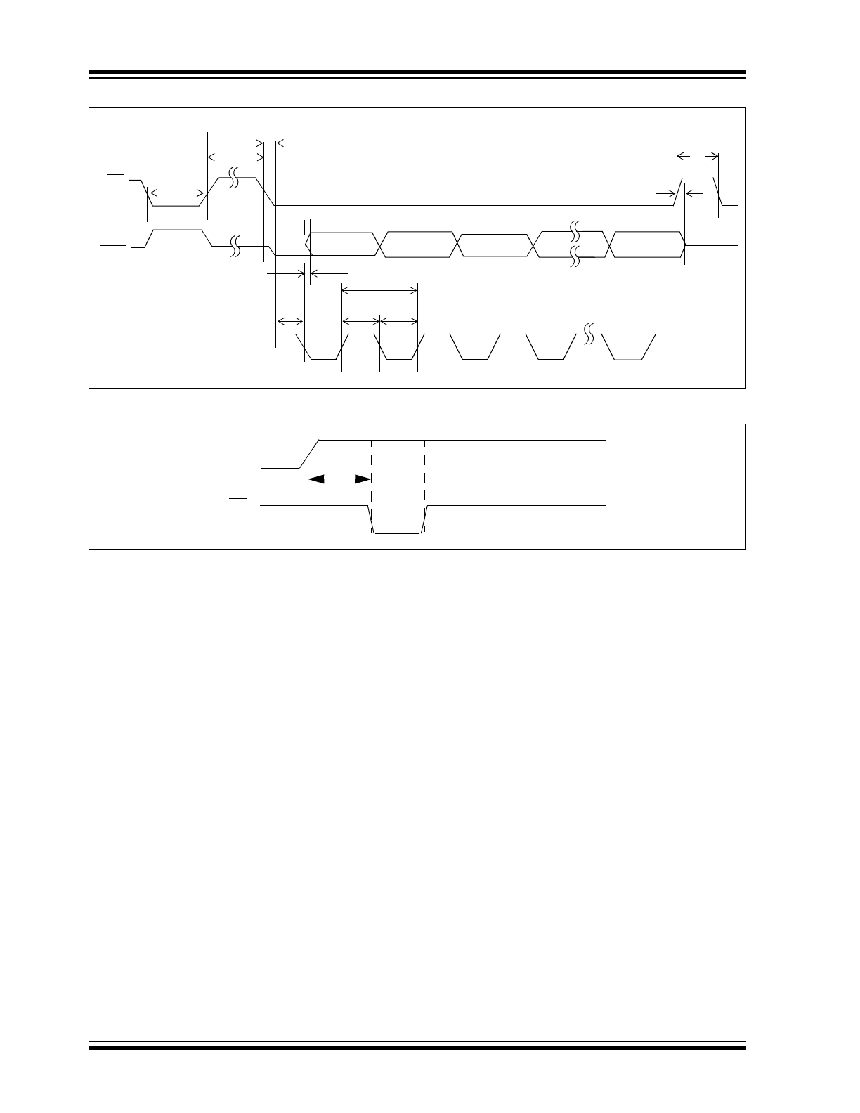
FIGURE 1-1:
Serial Timing.
FIGURE 1-2:
Power-Up Timing.
t
RDY
t
CSL
t
DO
t
SU
f
SCK
t
HI
t
LO
t
DIS
CS
SDO
SCK
t
CSD
t
CSHSD
/RDY
V
DD
CS
t
PUCSL
2005-2014 Microchip Technology Inc.
DS20001950F-page 7
MCP3550/1/3
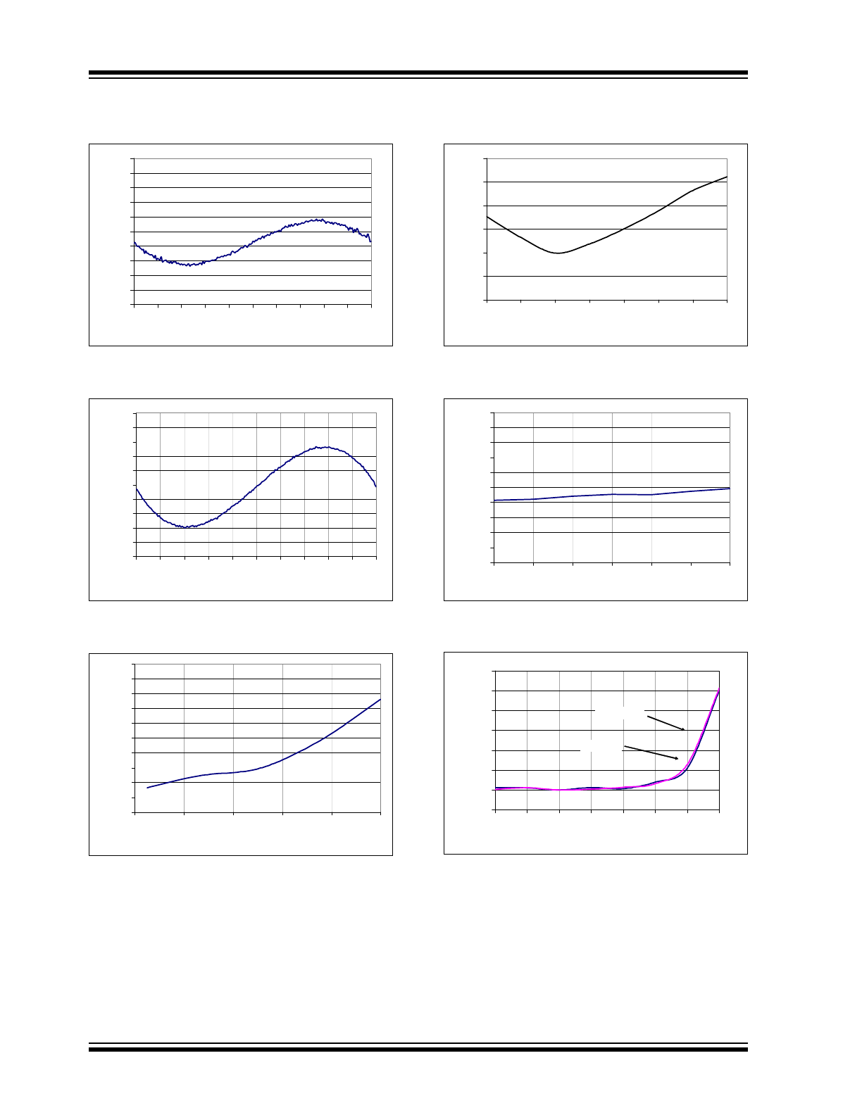
2.0
TYPICAL PERFORMANCE CURVES
Note:
Unless otherwise specified, T
A
= +25°C, V
DD
= 5V, V
REF
= 2.5V, V
SS
= 0V, V
CM
= V
REF
/2, V
IN
+ = V
IN
-.
All ppm units use 2*V
REF
as full scale range.
Unless otherwise noted, graphs apply to entire MCP3550/1/3 family.
FIGURE 2-1:
INL Error vs. Input Voltage
(V
DD
= 2.7V).
FIGURE 2-2:
INL Error vs. Input Voltage
(V
DD
= 5.0V).
FIGURE 2-3:
INL Error vs. Input Voltage
(V
DD
= 5.0V, V
REF
= 5V).
FIGURE 2-4:
Maximum INL Error vs.
V
REF
.
FIGURE 2-5:
Maximum INL Error vs.
Temperature.
FIGURE 2-6:
Output Noise vs. Input
Voltage (V
DD
= 2.7V).
Note:
The graphs and tables provided following this note are a statistical summary based on a limited number of
samples and are provided for informational purposes only. The performance characteristics listed herein
are not tested or guaranteed. In some graphs or tables, the data presented may be outside the specified
operating range (e.g., outside specified power supply range) and therefore outside the warranted range.
-5
-4
-3
-2
-1
0
1
2
3
4
5
-2.5
-1.5
-0.5
0.5
1.5
2.5
V
IN
(V)
IN
L
(
ppm
)
+125 C
+85 C
-40 C
+25 C
-5
-4
-3
-2
-1
0
1
2
3
4
5
-2.5
-1.5
-0.5
0.5
1.5
2.5
V
IN
(V)
IN
L (
p
p
m
)
+125 C
+85 C
+25 C
- 40 C
-10
-8
-6
-4
-2
0
2
4
6
8
10
-5
-4
-3
-2
-1
0
1
2
3
4
5
V
IN
(V)
IN
L (p
pm
)
+125 C
+85 C
+25 C
-40 C
0
2
4
6
8
10
0
0.5
1
1.5
2
2.5
3
3.5
4
4.5
5
V
REF
(V)
IN
L
Erro
r (
p
p
m
)
0
1
2
3
4
5
6
7
8
9
10
-50
-25
0
25
50
75
100
125
Temperature (°C)
Ma
x
I
N
L
(
p
p
m
)
0
1
2
3
4
5
6
7
8
9
10
-2.5
-1.5
-0.5
0.5
1.5
2.5
V
IN
(Volts)
O
u
tp
u
t No
ise (
µ
V
RM
S
)
MCP3553
MCP3550/1
MCP3550/1/3
DS20001950F-page 8
2005-2014 Microchip Technology Inc.
Note:
Unless otherwise specified, T
A
= +25°C, V
DD
= 5V, V
REF
= 2.5V, V
SS
= 0V, V
CM
= V
REF
/2, V
IN
+ = V
IN
-.
All ppm units use 2*V
REF
as full scale range. Unless otherwise noted, graphs apply to entire MCP3550/1/3 family.
FIGURE 2-7:
Output Noise vs. Input
Voltage (V
DD
= 5.0V).
u
FIGURE 2-8:
Output Noise vs. V
REF
.
FIGURE 2-9:
Output Noise vs.V
DD
.
FIGURE 2-10:
Output Noise vs.
Temperature.
FIGURE 2-11:
Offset Error vs V
DD
(V
CM
= 0V).
FIGURE 2-12:
Offset Error vs.
Temperature (V
REF
= 5.0V).
0
5
10
15
-2.5
-1.5
-0.5
0.5
1.5
2.5
V
IN
(V)
O
u
tp
u
t N
o
is
e
(
µ
V
RM
S
)
MCP3553
MCP3550/1
0.0
1.0
2.0
3.0
4.0
5.0
6.0
7.0
8.0
9.0
10.0
0.0
1.0
2.0
3.0
4.0
5.0
V
REF
(V)
O
u
tpu
t N
o
is
e (µV
RM
S
)
MCP3550/1
MCP3553
0
1
2
3
4
5
6
7
8
9
10
2.5
3
3.5
4
4.5
5
5.5
V
DD
(V)
O
u
tp
u
t N
o
is
e
(
µ
V
RM
S
)
MCP3550/1
MCP3553
0
1
2
3
4
5
6
7
8
9
10
-50
-25
0
25
50
75
100
125
Temperature (°C)
O
u
tpu
t N
o
is
e
(µ
V
RM
S
)
MCP3550/1
MCP3553
0
1
2
3
4
5
2.5
3
3.5
4
4.5
5
5.5
V
DD
(V)
O
ffs
e
t (µ
V
)
0
1
2
3
4
5
6
7
-50
-25
0
25
50
75
100
125
Temperature (°C)
Of
fs
e
t (
µ
V)
2005-2014 Microchip Technology Inc.
DS20001950F-page 9
MCP3550/1/3
Note:
Unless otherwise specified, T
A
= +25°C, V
DD
= 5V, V
REF
= 2.5V, V
SS
= 0V, V
CM
= V
REF
/2, V
IN
+ = V
IN
-.
All ppm units are ratioed against 2*V
REF .
Unless otherwise noted, graphs apply to entire MCP3550/1/3 family.
FIGURE 2-13:
Full Scale Error vs. V
DD
.
FIGURE 2-14:
Full Scale Error vs.
Temperature.
FIGURE 2-15:
Full Scale Error vs.
Temperature (V
REF
= 5.0V).
FIGURE 2-16:
MCP3550/1 Output Noise
Histogram.
FIGURE 2-17:
MCP3553 Output Noise
Histogram.
FIGURE 2-18:
Total Unadjusted Error
(TUE) vs. Input Voltage (V
DD
= 2.7V).
-5
-4
-3
-2
-1
0
1
2
3
4
5
2.5
3
3.5
4
4.5
5
5.5
V
DD
(V)
F
u
ll
Sc
al
e
Er
ro
r (p
p
m
)
Positive Full Scale
Negative Full Scale
-10
-8
-6
-4
-2
0
2
4
6
8
10
-50
-25
0
25
50
75
100
125
Temperature (°C)
F
u
ll
Scale Er
ro
r
(p
p
m
)
Positive Full Scale
Negative Full Scale
-10
-8
-6
-4
-2
0
2
4
6
8
10
-50
-25
0
25
50
75
100
125
Temperature (°C)
Ful
l S
c
a
le
E
rr
o
r
(ppm)
Positive Full Scale
Negative Full Scale
0
500
1000
1500
2000
2500
3000
3500
4000
-15
-10
-5
0
5
10
15
Number of Occurrences
Output Code (LSB)
V
DD
= 5V
V
REF
= 2.5V
V
CM
= 1.25V
V
IN
= 0V
T
A
= 25C
16384
consecutive
readings
0
200
400
600
800
1000
1200
1400
1600
1800
-15
-10
-5
0
5
10
15
Output Code (LSB)
Nu
m
b
er
o
f
O
c
c
u
rr
e
n
c
e
s
V
DD
= 5V
V
REF
= 2.5V
V
CM
= 1.25V
V
IN
= 0V
T
A
= 25°C
16384
consecutive
readings
-5.0
-4.0
-3.0
-2.0
-1.0
0.0
1.0
2.0
3.0
4.0
5.0
-2.5 -2.0 -1.5 -1.0 -0.5 0.0 0.5 1.0 1.5 2.0 2.5
V
IN
(V)
TU
E
(
p
pm
)
MCP3550/1/3
DS20001950F-page 10
2005-2014 Microchip Technology Inc.
Note:
Unless otherwise specified, T
A
= +25°C, V
DD
= 5V, V
REF
= 2.5V, V
SS
= 0V, V
CM
= V
REF
/2, V
IN
+ = V
IN
-.
All ppm units use 2*V
REF
as full scale range
.
Unless otherwise noted, graphs apply to entire MCP3550/1/3 family.
FIGURE 2-19:
Total Unadjusted Error
(TUE) vs. Input Voltage.
FIGURE 2-20:
Total Unadjusted Error
(TUE) vs. Input Voltage (V
REF
= 5.0V).
FIGURE 2-21:
Maximum TUE vs. V
REF
.
FIGURE 2-22:
Maximum TUE vs.
Temperature.
FIGURE 2-23:
Maximum TUE vs. V
DD
.
FIGURE 2-24:
I
DDS
vs. Temperature.
-5
-4
-3
-2
-1
0
1
2
3
4
5
-2.5
-2
-1.5
-1
-0.5
0
0.5
1
1.5
2
2.5
V
IN
(V)
TU
E
(
p
p
m
)
-10
-8
-6
-4
-2
0
2
4
6
8
10
-5
-4
-3
-2
-1
0
1
2
3
4
5
V
IN
(V)
TUE
(p
pm
)
0
1
2
3
4
5
6
7
8
9
10
0
1
2
3
4
5
V
REF
(V)
M
a
x
imu
m T
U
E
(
p
p
m
)
0
1
2
3
4
5
6
-50
-25
0
25
50
75
100
125
Temperature (°C)
M
axi
mu
m TU
E
(
p
p
m
)
0
0.5
1
1.5
2
2.5
3
3.5
4
4.5
5
2.5
2.7
3
3.3
4
5
5.5
V
DD
(V)
TU
E
(p
p
m
)
-0.1
0
0.1
0.2
0.3
0.4
0.5
0.6
-50
-25
0
25
50
75
100
125
Temperature (°C)
I
DDS
(µ
A
)
MCP3550/1
MCP3553