
2001-2011 Microchip Technology Inc.
DS21700E-page 1
MCP3301
Features
• Full Differential Inputs
• ±1 LSB max DNL
• ±1 LSB max INL (MCP3301-B)
• ±2 LSB max INL (MCP3301-C)
• Single supply operation: 4.5V to 5.5V
• 100 ksps sampling rate with 5V supply voltage
• 50 nA typical standby current, 1 µA max
• 450 µA max active current at 5V
• Industrial temp range: -40°C to +85°C
• 8-pin MSOP, PDIP, and SOIC packages
• Mixed Signal PICtail™ Demo Board (P/N:
MXSIGDM) compatible
Applications
• Remote Sensors
• Battery-operated Systems
• Transducer Interface
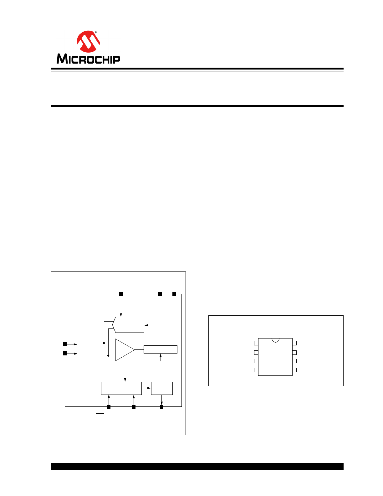
Functional Block Diagram
General Description
The MCP3301 13-bit analog-to-digital (A/D) converter
features full differential inputs and low power consump-
tion in a small package that is ideal for battery-powered
systems and remote data acquisition applications.
Incorporating a successive approximation architecture
with on-board sample and hold circuitry, the 13-bit A/D
converter is specified to have ±1 LSB Differential Non-
linearity (DNL) and ±1 LSB Integral Nonlinearity (INL)
for B-grade devices and ±2 LSB for C-grade devices.
The industry-standard SPI serial interface enables 13-
bit A/D converter capability to be added to any PIC
®
microcontroller.
The MCP3301 features a low current design that per-
mits operation with typical standby and active currents
of only 50 nA and 300 µA, respectively. The device is
capable of conversion rates of up to 100 ksps with
tested specifications over a 4.5V to 5.5V supply range.
The reference voltage can be varied from 400 mV to
5V, yielding input-referred resolution between 98 µV
and 1.22 mV.
The MCP3301 is available in 8-pin PDIP, 150 mil SOIC,
and MSOP packages. The full differential inputs of this
device enable a wide variety of signals to be used in
applications such as remote data acquisition, portable
instrumentation, and battery-operated applications.
Package Types
Comparator
13-Bit SAR
CDAC
Control Logic
CS/SHDN
V
REF
V
SS
V
DD
CLK
D
OUT
Shift
Register
IN+
IN-
+
-
& Hold
Circuits
Sample
MSOP, PDIP, SOIC
V
DD
CS/SHDN
CLK
V
REF
IN(+)
IN(-)
V
SS
D
OUT
M
C
P330
1
1
2
3
4
8
7
6
5
13-Bit Differential Input, Low Power A/D Converter
with SPI Serial Interface
MCP3301
DS21700E-page 2
2001-2011 Microchip Technology Inc.
1.0
ELECTRICAL
CHARACTERISTICS
Maximum Ratings*
V
DD
...................................................................................7.0V
All inputs and outputs w.r.t. V
SS
............... -0.3V to V
DD
+0.3V
Storage temperature .....................................-65°C to +150°C
Ambient temperature with power applied......-65°C to +125°C
Maximum Junction Temperature .................................. 150°C
ESD protection on all pins (HBM) .................................> 4 kV
*Notice: Stresses above those listed under “Maximum
ratings” may cause permanent damage to the device. This is
a stress rating only and functional operation of the device at
those or any other conditions above those indicated in the
operational listings of this specification is not implied.
Exposure to maximum rating conditions for extended periods
may affect device reliability.
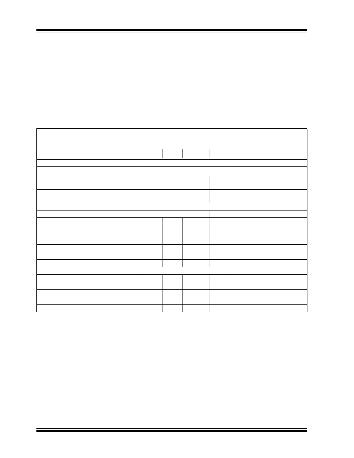
ELECTRICAL CHARACTERISTICS
Electrical Characteristics: Unless otherwise noted, all parameters apply at V
DD
= 5V, V
SS
= 0V, and V
REF
= 5V. Full differential
input configuration (
Figure 1-5
) with fixed common mode voltage of 2.5V. All parameters apply over temperature with
T
AMB
= -40°C to +85°C (
Note 7
). Conversion speed (
F
SAMPLE)
is 100 ksps with
F
CLK
= 17*
F
SAMPLE
Parameter
Symbol
Min
Typ
Max
Units
Conditions
Conversion Rate
Maximum Sampling Frequency
F
SAMPLE
—
—
100
ksps See
F
CLK
specifications (
Note 8
)
Conversion Time
t
CONV
13
CLK
periods
Acquisition Time
t
ACQ
1.5
CLK
periods
DC Accuracy
Resolution
12 data bits + sign
bits
Integral Nonlinearity
INL
—
—
±0.5
±1
±1
±2
LSB
MCP3301-B
MCP3301-C
Differential Nonlinearity
DNL
—
±0.5
±1
LSB
Monotonic with no missing codes over
temperature
Positive Gain Error
-3
-0.75
+2
LSB
Negative Gain Error
-3
-0.5
+2
LSB
Offset Error
-3
+3
+6
LSB
Dynamic Performance
Total Harmonic Distortion
THD
—
-91
—
dB
Note 3
Signal to Noise and Distortion
SINAD
—
78
—
dB
Note 3
Spurious Free Dynamic Range
SFDR
—
92
—
dB
Note 3
Common-Mode Rejection
CMRR
—
79
—
dB
Note 6
Power Supply Rejection
PSR
—
74
—
dB
Note 4
Note 1: This specification is established by characterization and not 100% tested.
2: See characterization graphs that relate converter performance to V
REF
level.
3: V
IN
= 0.1V to 4.9V @ 1 kHz.
4: V
DD
= 5V DC ±500 mV
P-P
@ 1 kHz, see test circuit
Figure 1-4
.
5: Maximum clock frequency specification must be met.
6: V
REF
= 400 mV, V
IN
= 0.1V to 4.9V @ 1 kHz
7: MSOP devices are only specified at 25°C and +85°C.
8: For slow sample rates, see
Section 5.2.1 “Maintaining Minimum Clock Speed”
for limitations on clock frequency.
9: 4.5V - 5.5V is the supply voltage range for specified performance
2001-2011 Microchip Technology Inc.
DS21700E-page 3
MCP3301
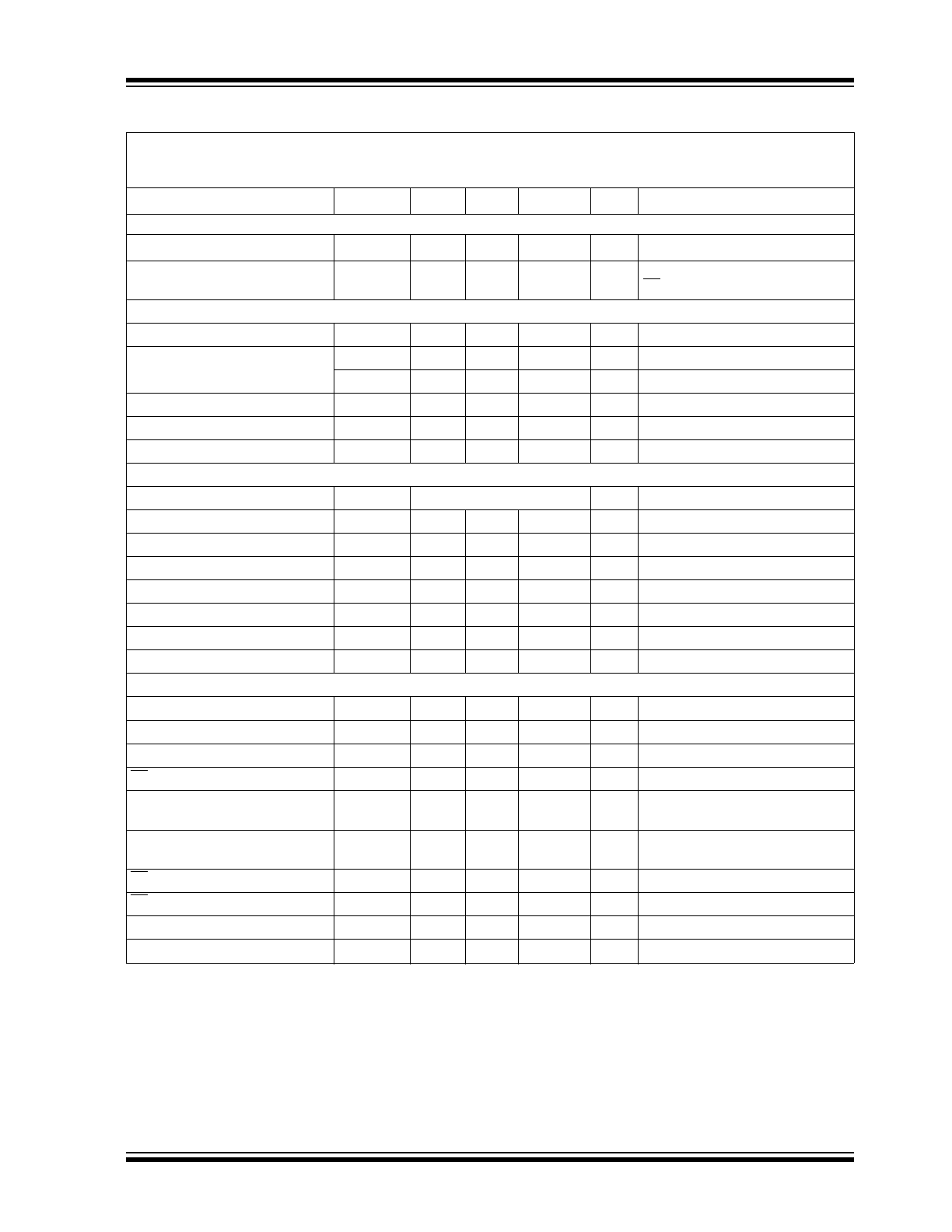
Reference Input
Voltage Range
0.4
—
V
DD
V
Note 2
Current Drain
—
—
100
0.001
150
3
µA
µA
CS = V
DD
= 5V
Analog Inputs
Full-Scale Input Span
IN(+)-IN(-)
-V
REF
—
V
REF
V
Absolute Input Voltage
IN(+)
-0.3
—
V
DD
+ 0.3
V
IN(-)
-0.3
—
V
DD
+ 0.3
V
Leakage Current
—
0.001
±1
µA
Switch Resistance
R
S
—
1
—
k
See
Figure 5-3
Sample Capacitor
C
SAMPLE
—
25
—
pF
See
Figure 5-3
Digital Input/Output
Data Coding Format
Binary Two’s Complement
High Level Input Voltage
V
IH
0.7 V
DD
—
—
V
Low Level Input Voltage
V
IL
—
—
0.3 V
DD
V
High Level Output Voltage
V
OH
4.1
—
—
V
I
OH
= -1 mA, V
DD
= 4.5V
Low Level Output Voltage
V
OL
—
—
0.4
V
I
OL
= 1 mA, V
DD
= 4.5V
Input Leakage Current
I
LI
-10
—
10
µA
V
IN
= V
SS
or V
DD
Output Leakage Current
I
LO
-10
—
10
µA
V
OUT
= V
SS
or V
DD
Pin Capacitance
C
IN
, C
OUT
—
—
10
pF
T
AMB
= 25°C, f = 1 MHz,
Note 1
Timing Specifications
Clock Frequency (Note 8)
F
CLK
0.085
—
1.7
MHz V
DD
= 5V,
F
SAMPLE
= 100 ksps
Clock High Time
t
HI
275
—
—
ns
Note 5
Clock Low Time
t
LO
275
—
—
ns
Note 5
CS Fall To First Rising CLK Edge
t
SUCS
100
—
—
ns
CLK Fall To Output Data Valid
t
DO
—
—
125
200
ns
ns
V
DD
= 5V, see
Figure 1-2
V
DD
= 2.7V, see
Figure 1-2
CLK Fall To Output Enable
t
EN
—
—
125
200
ns
ns
V
DD
= 5V, see
Figure 1-2
V
DD
= 2.7V, see
Figure 1-2
CS Rise To Output Disable
t
DIS
—
—
100
ns
See test circuits,
Figure 1-2
;
Note 1
CS Disable Time
t
CSH
580
—
—
ns
D
OUT
Rise Time
t
R
—
—
100
ns
See test circuits,
Figure 1-2
;
Note 1
D
OUT
Fall Time
t
F
—
—
100
ns
See test circuits,
Figure 1-2
;
Note 1
ELECTRICAL CHARACTERISTICS (CONTINUED)
Electrical Characteristics: Unless otherwise noted, all parameters apply at V
DD
= 5V, V
SS
= 0V, and V
REF
= 5V. Full differential
input configuration (
Figure 1-5
) with fixed common mode voltage of 2.5V. All parameters apply over temperature with
T
AMB
= -40°C to +85°C (
Note 7
). Conversion speed (
F
SAMPLE)
is 100 ksps with
F
CLK
= 17*
F
SAMPLE
Parameter
Symbol
Min
Typ
Max
Units
Conditions
Note 1: This specification is established by characterization and not 100% tested.
2: See characterization graphs that relate converter performance to V
REF
level.
3: V
IN
= 0.1V to 4.9V @ 1 kHz.
4: V
DD
= 5V DC ±500 mV
P-P
@ 1 kHz, see test circuit
Figure 1-4
.
5: Maximum clock frequency specification must be met.
6: V
REF
= 400 mV, V
IN
= 0.1V to 4.9V @ 1 kHz
7: MSOP devices are only specified at 25°C and +85°C.
8: For slow sample rates, see
Section 5.2.1 “Maintaining Minimum Clock Speed”
for limitations on clock frequency.
9: 4.5V - 5.5V is the supply voltage range for specified performance
MCP3301
DS21700E-page 4
2001-2011 Microchip Technology Inc.
.
FIGURE 1-1:
Timing Parameters.
Power Requirements
Operating Voltage
V
DD
4.5
—
5.5
V
Note 9
Operating Current
I
DD
—
—
300
200
450
—
µA
V
DD ,
V
REF
= 5V, D
OUT
unloaded
V
DD
, V
REF
= 2.7V, D
OUT
unloaded
Standby Current
I
DDS
—
0.05
1
µA
CS = V
DD
= 5.0V
Temperature Ranges
Specified Temperature Range
T
A
-40
—
+85
°C
Operating Temperature Range
T
A
-40
—
+85
°C
Storage Temperature Range
T
A
-65
—
+150
°C
Thermal Package Resistance
Thermal Resistance, 8L-MSOP
JA
—
206
—
°C/W
Thermal Resistance, 8L-PDIP
JA
—
85
—
°C/W
Thermal Resistance, 8L-SOIC
JA
—
163
—
°C/W
ELECTRICAL CHARACTERISTICS (CONTINUED)
Electrical Characteristics: Unless otherwise noted, all parameters apply at V
DD
= 5V, V
SS
= 0V, and V
REF
= 5V. Full differential
input configuration (
Figure 1-5
) with fixed common mode voltage of 2.5V. All parameters apply over temperature with
T
AMB
= -40°C to +85°C (
Note 7
). Conversion speed (
F
SAMPLE)
is 100 ksps with
F
CLK
= 17*
F
SAMPLE
Parameter
Symbol
Min
Typ
Max
Units
Conditions
Note 1: This specification is established by characterization and not 100% tested.
2: See characterization graphs that relate converter performance to V
REF
level.
3: V
IN
= 0.1V to 4.9V @ 1 kHz.
4: V
DD
= 5V DC ±500 mV
P-P
@ 1 kHz, see test circuit
Figure 1-4
.
5: Maximum clock frequency specification must be met.
6: V
REF
= 400 mV, V
IN
= 0.1V to 4.9V @ 1 kHz
7: MSOP devices are only specified at 25°C and +85°C.
8: For slow sample rates, see
Section 5.2.1 “Maintaining Minimum Clock Speed”
for limitations on clock frequency.
9: 4.5V - 5.5V is the supply voltage range for specified performance
CS
CLK
t
SUCS
t
CSH
t
HI
t
LO
D
OUT
t
EN
t
DO
t
R
t
F
LSB
Sign Bit
t
DIS
Null Bit
HI-Z
HI-Z
2001-2011 Microchip Technology Inc.
DS21700E-page 5
MCP3301
1.1
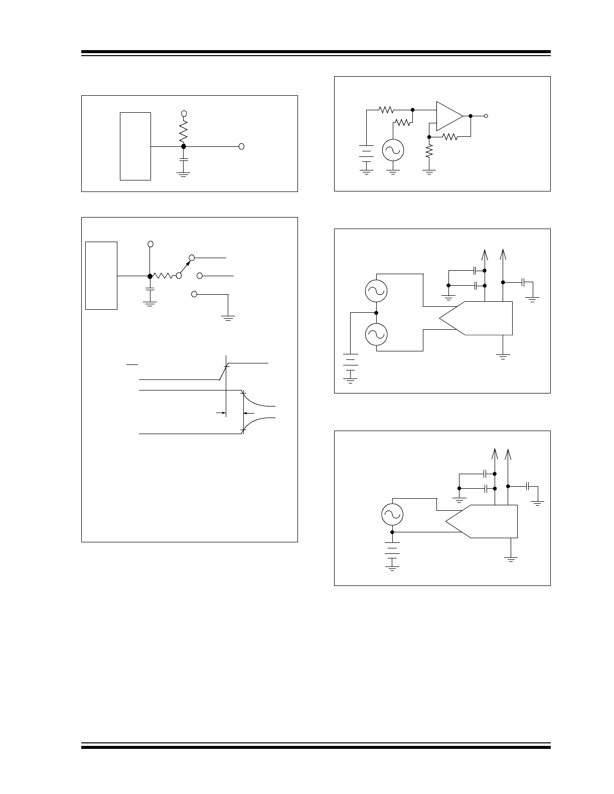
Test Circuits
FIGURE 1-2:
Load Circuit for t
R
, t
F
,
t
DO.
FIGURE 1-3:
Load Circuit for T
DIS
and
T
EN
.
FIGURE 1-4:
Power Supply Sensitivity
Test Circuit (PSRR).
FIGURE 1-5:
Full Differential Test
Configuration Example.
FIGURE 1-6:
Pseudo Differential Test
Configuration Example.
Test Point
1.4V
D
OUT
3 k
C
L
= 100 pF
MC
P
3301
*Waveform 1 is for an output with internal
conditions such that the output is high, unless
disabled by the output control.
†Waveform 2 is for an output with internal
conditions such that the output is low, unless
disabled by the output control.
V
IH
T
DIS
CS
D
OUT
Waveform 1*
D
OUT
Waveform 2†
90%
10%
Voltage Waveforms for t
DIS
Test Point
D
OUT
3 k
100 pF
t
DIS
Waveform 2
t
DIS
Waveform 1
t
EN
Waveform
V
DD
V
DD
/2
V
SS
MCP
330
1
2.63V
-
+
1 k
5V ±500 mVp-p
5V
P-P
1 k
20 k
To V
DD
on DUT
1 k
1/2 MCP602
V
DD
= 5V
0.1 µF
IN(+)
IN(-)
MCP3301
5V
P-P
V
REF
= 5V
5V
P-P
V
CM
= 2.5V
1 µF
0.1 µF
V
REF
V
DD
V
SS
0.1 µF
IN(+)
IN(-)
MCP3301
V
DD
=5V
V
CM
=2.5V
5V
P-P
V
REF
=2.5V
1 µF
0.1 µF
V
REF
V
DD
V
SS
MCP3301
DS21700E-page 6
2001-2011 Microchip Technology Inc.
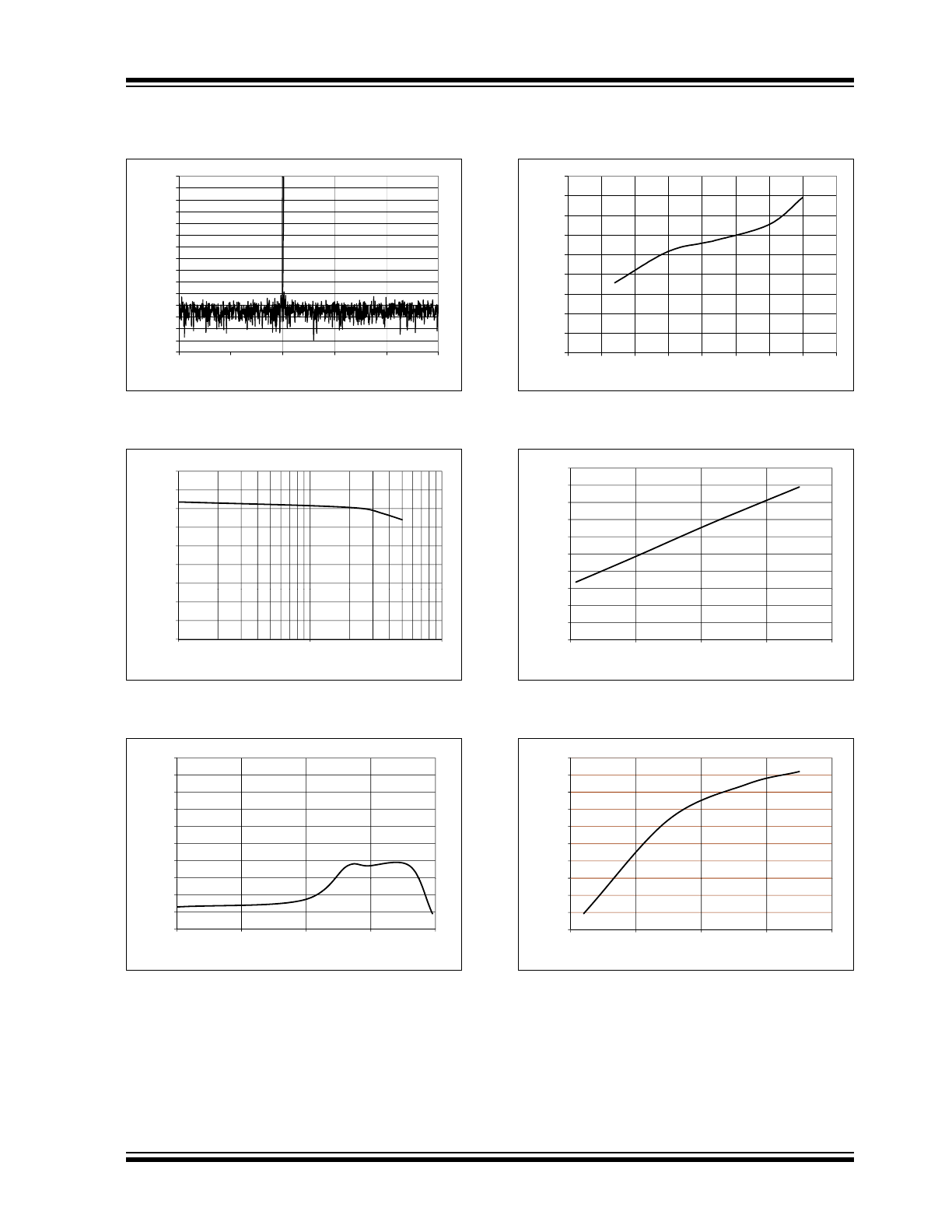
2.0
TYPICAL PERFORMANCE CURVES
Note: Unless otherwise indicated, V
DD
= V
REF
= 5V, Full differential input configuration, V
SS
= 0V, F
SAMPLE
= 100 ksps,
F
CLK
= 17*F
SAMPLE
, T
A
= 25°C.
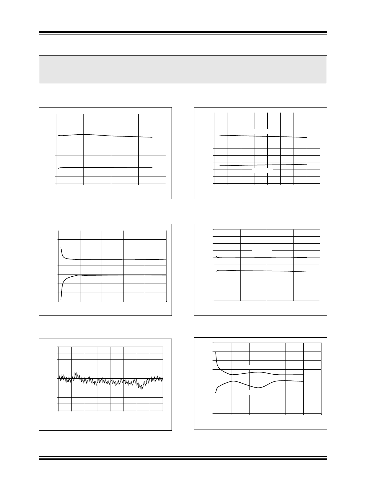
FIGURE 2-1:
Integral Nonlinearity (INL)
vs. Sample Rate.
FIGURE 2-2:
Integral Nonlinearity (INL)
vs. V
REF.
FIGURE 2-3:
Integral Nonlinearity (INL)
vs. Code (Representative Part).
FIGURE 2-4:
Integral Nonlinearity (INL)
vs. Temperature.
FIGURE 2-5:
Differential Nonlinearity
(DNL) vs. Sample Rate.
FIGURE 2-6:
Differential Nonlinearity
(DNL) vs. V
REF
.
Note:
The graphs and tables provided following this note are a statistical summary based on a limited number of
samples and are provided for informational purposes only. The performance characteristics listed herein
are not tested or guaranteed. In some graphs or tables, the data presented may be outside the specified
operating range (e.g., outside specified power supply range) and therefore outside the warranted range.
-1.0
-0.8
-0.6
-0.4
-0.2
0.0
0.2
0.4
0.6
0.8
1.0
0
50
100
150
200
Sample Rate (ksps)
IN
L(LSB
)
Positive INL
Negative INL
-2.0
-1.5
-1.0
-0.5
0.0
0.5
1.0
1.5
2.0
0
1
2
3
4
5
V
REF
(V)
INL (LSB)
Positive INL
Negative INL
-1
-0.8
-0.6
-0.4
-0.2
0
0.2
0.4
0.6
0.8
1
-4096
-3072
-2048
-1024
0
1024
2048
3072
4096
Code
IN
L(LSB
)
-1.0
-0.8
-0.6
-0.4
-0.2
0.0
0.2
0.4
0.6
0.8
1.0
-50
-25
0
25
50
75
100
125
150
Temperature(°C)
IN
L(LSB
)
Positive INL
Negative INL
-1.0
-0.8
-0.6
-0.4
-0.2
0.0
0.2
0.4
0.6
0.8
1.0
0
50
100
150
200
Sample Rate(ksps)
DNL
(L
SB)
Positive INL
Negative INL
-2.0
-1.5
-1.0
-0.5
0.0
0.5
1.0
1.5
2.0
0
1
2
3
4
5
6
V
REF
(V)
DNL
(L
SB)
Positive INL
Negative INL
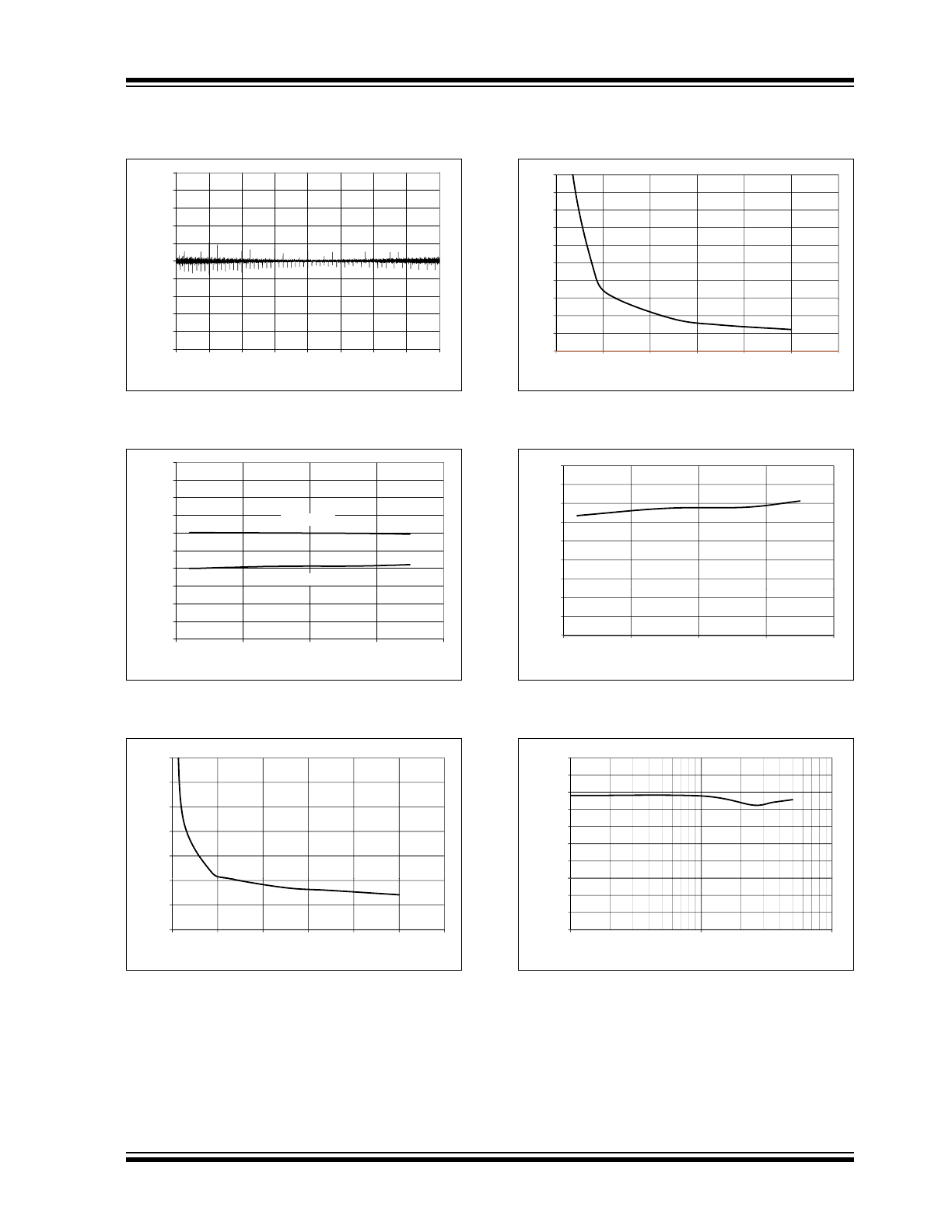
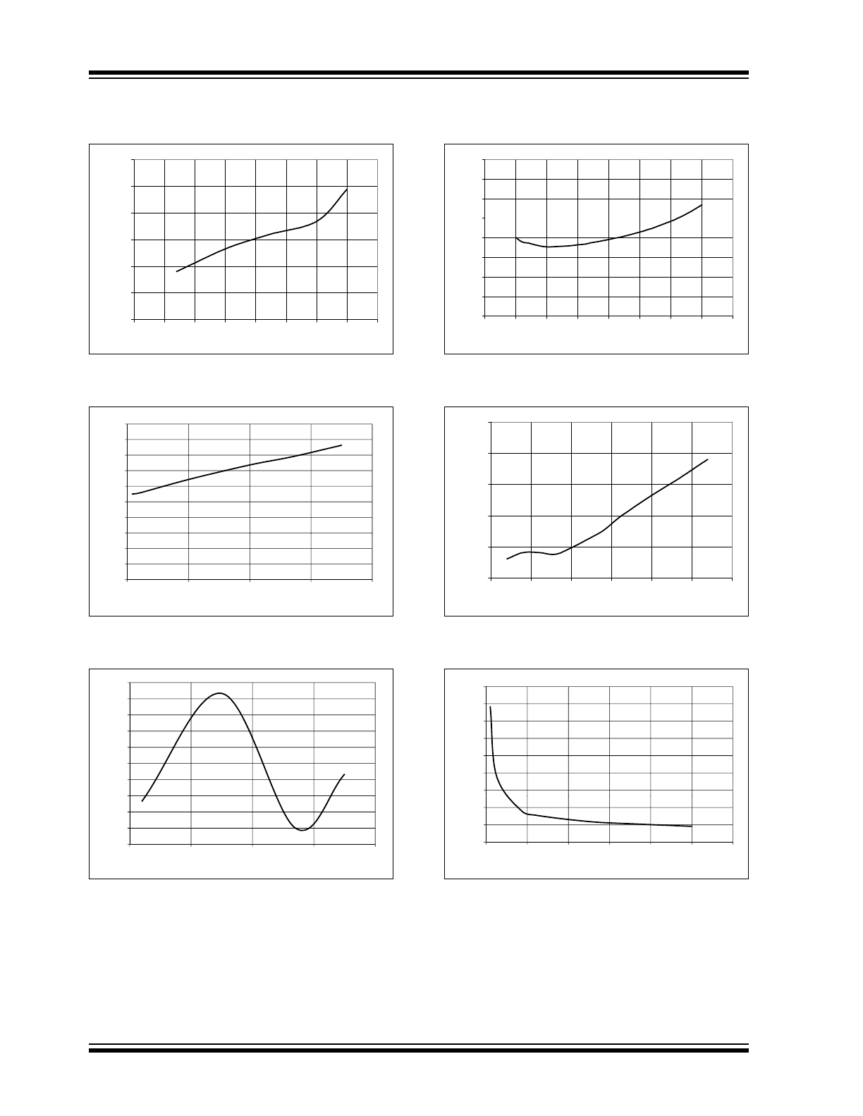
2001-2011 Microchip Technology Inc.
DS21700E-page 7
MCP3301
Note: Unless otherwise indicated, V
DD
= V
REF
= 5V, Full differential input configuration, V
SS
= 0V, F
SAMPLE
= 100 ksps,
F
CLK
= 17*F
SAMPLE
, T
A
= 25°C.
FIGURE 2-7:
Differential Nonlinearity
(DNL) vs. Code (Representative Part).
FIGURE 2-8:
Differential Nonlinearity
(DNL) vs. Temperature.
FIGURE 2-9:
Positive Gain Error vs. V
REF
.
FIGURE 2-10:
Offset Error vs. V
REF
.
FIGURE 2-11:
Positive Gain Error vs.
Temperature.
FIGURE 2-12:
Signal to Noise Ratio (SNR)
vs. Input Frequency.
-1
-0.8
-0.6
-0.4
-0.2
0
0.2
0.4
0.6
0.8
1
-4096
-3072
-2048
-1024
0
1024
2048
3072
4096
Code
DNL
(L
SB)
-1.0
-0.8
-0.6
-0.4
-0.2
0.0
0.2
0.4
0.6
0.8
1.0
-50
0
50
100
150
Temperature (°C)
DNL
Erro
r (L
SB)
Positive DNL
Negative DNL
0
1
2
3
4
5
itiv
e Gain Error (LSB)
-2
-1
0
0
1
2
3
4
5
6
Pos
i
V
REF
(V)
6
8
10
12
14
16
18
20
O
ffset Error
(LSB)
0
2
4
6
0
1
2
3
4
5
6
O
V
REF
(V)
-1.2
-1.0
-0.8
-0.6
-0.4
-0.2
0.0
s
itiv
e Gain Error (LSB)
-1.8
-1.6
-1.4
-50
0
50
100
150
Po
s
Temperature (°C)
30
40
50
60
70
80
90
100
SNR (dB)
0
10
20
30
1
10
100
Input Frequency (kHz)
MCP3301
DS21700E-page 8
2001-2011 Microchip Technology Inc.
Note: Unless otherwise indicated, V
DD
= V
REF
= 5V, Full differential input configuration, V
SS
= 0V, F
SAMPLE
= 100 ksps,
F
CLK
= 17*F
SAMPLE
, T
A
= 25°C.
FIGURE 2-13:
Total Harmonic Distortion
(THD) vs. Input Frequency.
FIGURE 2-14:
Offset Error vs.
Temperature.
FIGURE 2-15:
Signal to Noise and
Distortion (SINAD) vs. Input Frequency.
FIGURE 2-16:
Signal to Noise and
Distortion (SINAD) vs. Input Signal Level.
FIGURE 2-17:
Effective Number of Bits
(ENOB) vs. V
REF
.
FIGURE 2-18:
Spurious Free Dynamic
Range (SFDR) vs. Input Frequency.
-70
-60
-50
-40
-30
-20
-10
0
THD (dB)
-100
-90
-80
-70
1
10
100
Input Frequency (kHz)
1
1.5
2
2.5
3
3.5
O
ffset Error
(LSB)
0
0.5
1
-50
0
50
100
150
O
Temperature (°C)
30
40
50
60
70
80
90
SINAD (dB)
0
10
20
1
10
100
Input Frequency (kHz)
30
40
50
60
70
80
SINAD (dB)
0
10
20
-40
-35
-30
-25
-20
-15
-10
-5
0
Input Signal Level (dB)
9
10
11
12
13
ENOB (rms)
7
8
0
1
2
3
4
5
6
V
REF
(V)
30
40
50
60
70
80
90
100
SFDR (dB)
0
10
20
30
1
10
100
Input Frequency (kHz)
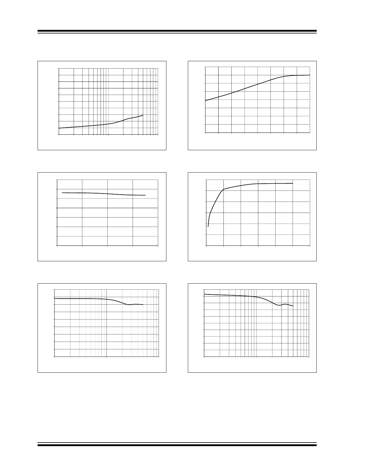
2001-2011 Microchip Technology Inc.
DS21700E-page 9
MCP3301
Note: Unless otherwise indicated, V
DD
= V
REF
= 5V, Full differential input configuration, V
SS
= 0V, F
SAMPLE
= 100 ksps,
F
CLK
= 17*F
SAMPLE
, T
A
= 25°C.
FIGURE 2-19:
Frequency Spectrum of
10 kHz Input (Representative Part).
FIGURE 2-20:
Effective Number of Bits
(ENOB) vs. Input Frequency.
FIGURE 2-21:
Power Supply Rejection
(PSR) vs. Ripple Frequency. A 0.1
µ
F bypass
capacitor is connected to the V
DD
pin.
FIGURE 2-22:
I
DD
vs. V
DD
.
FIGURE 2-23:
I
DD
vs. Sample Rate.
FIGURE 2-24:
I
DD
vs. Temperature.
-150
-140
-130
-120
-110
-100
-90
-80
-70
-60
-50
-40
-30
-20
-10
0
0
5000
10000
15000
20000
25000
Frequency (Hz)
A
m
plitude (dB
)
11.8
12
12.2
12.4
12.6
12.8
13
ENOB (rms)
11.2
11.4
11.6
1
10
100
Input Frequency (kHz)
-65
-60
-55
-50
-45
-40
-35
-30
PSR(dB)
-80
-75
-70
-65
1
10
100
1000
10000
Ripple Frequency (kHz)
0
50
100
150
200
250
300
350
400
450
2
2.5
3
3.5
4
4.5
5
5.5
6
V
DD
(V)
I
DD
(µ
A)
150
200
250
300
350
400
450
500
I
DD
(µA)
0
50
100
150
0
50
100
150
200
Sample Rate (ksps)
310
315
320
325
330
335
340
345
I
DD
(µA)
295
300
305
310
-50
0
50
100
150
Temperature (°C)
MCP3301
DS21700E-page 10
2001-2011 Microchip Technology Inc.
Note: Unless otherwise indicated, V
DD
= V
REF
= 5V, Full differential input configuration, V
SS
= 0V, F
SAMPLE
= 100 ksps,
F
CLK
= 17*F
SAMPLE
, T
A
= 25°C.
FIGURE 2-25:
I
REF
vs. V
DD
.
FIGURE 2-26:
I
REF
vs. Sample Rate.
FIGURE 2-27:
I
REF
vs. Temperature.
FIGURE 2-28:
I
DDS
vs. V
DD
.
FIGURE 2-29:
I
DDS
vs. Temperature.
FIGURE 2-30:
Negative Gain Error vs.
Reference Voltage.
0
20
40
60
80
100
120
2
2.5
3
3.5
4
4.5
5
5.5
6
V
DD
(V)
I
REF
(µ
A)
30
40
50
60
70
80
90
100
I
REF
(µA)
0
10
20
30
0
50
100
150
200
Sample Rate (ksps)
72 4
72.6
72.8
73
73.2
73.4
73.6
73.8
I
REF
(µA)
71.8
72
72.2
72.4
-50
0
50
100
150
Temperature (°C)
0
10
20
30
40
50
60
70
80
2
2.5
3
3.5
4
4.5
5
5.5
6
V
DD
(V)
I
DDS
(pA)
0.001
0.01
0.1
1
10
100
-50
-25
0
25
50
75
100
Temperature (°C)
I
DDS
(nA)
2
3
4
5
6
7
8
a
tiv
e
Gain Error (LSB)
-1
0
1
0
1
2
3
4
5
6
Neg
a
V
REF
(V)