2003-2017 Microchip Technology Inc.
DS20001805C-page 1
MCP3021
Features
• 10-bit Resolution
• ±1 LSB DNL, ±1 LSB INL maximum
• 250 µA Max Conversion Current
• 5 nA Typical Standby Current, 1 µA maximum
• I
2
C Compatible Serial Interface
- 100 kHz I
2
C Standard mode
- 400 kHz I
2
C Fast mode
• Up to 8 Devices on a Single 2-wire Bus
• 22.3 ksps in I
2
C Fast mode
• Single-Ended Analog Input Channel
• On-Chip Sample and Hold
• On-Chip Conversion Clock
• Single-Supply Specified Operation: 2.7V to 5.5V
• Temperature Range:
- Extended: -40°C to +125°C
• Small SOT-23-5 Package
Applications
• Data Logging
• Multi-Zone Monitoring
• Handheld Portable Applications
• Battery-Powered Test Equipment
• Remote or Isolated Data Acquisition
General Description
Microchip’s MCP3021 is a successive approximation
A/D converter (ADC) with a 10-bit resolution. Available
in the SOT-23 package, this device provides one
single-ended input with very low-power consumption.
Based on an advanced CMOS technology, the
MCP3021 provides a low maximum conversion current
and standby current of 250 µA and 1 µA, respectively.
Low-current consumption, combined with the small
SOT-23 package, make this device ideal for bat-
tery-powered and remote data acquisition applications.
Communication to the MCP3021 is performed using a
2-wire I
2
C compatible interface. Standard (100 kHz)
and Fast (400 kHz) I
2
C modes are available with the
device. An on-chip conversion clock enables indepen-
dent timing for the I
2
C and conversion clocks. The
device is also addressable, allowing up to eight devices
on a single 2-wire bus.
The MCP3021 runs on a single-supply voltage that
operates over a broad range of 2.7V to 5.5V. This
device also provides excellent linearity of ±1 LSB
differential nonlinearity (DNL) and ±1 LSB integral
nonlinearity (INL), maximum.
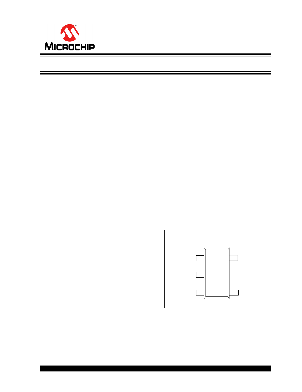
Package Type
5-Pin SOT-23
SCL
A
IN
1
2
3
5
SDA
V
SS
V
DD
4
MCP3
021
Low-Power 10-Bit A/D Converter with I
2
C Interface
MCP3021
DS20001805C-page 2
2003-2017 Microchip Technology Inc.
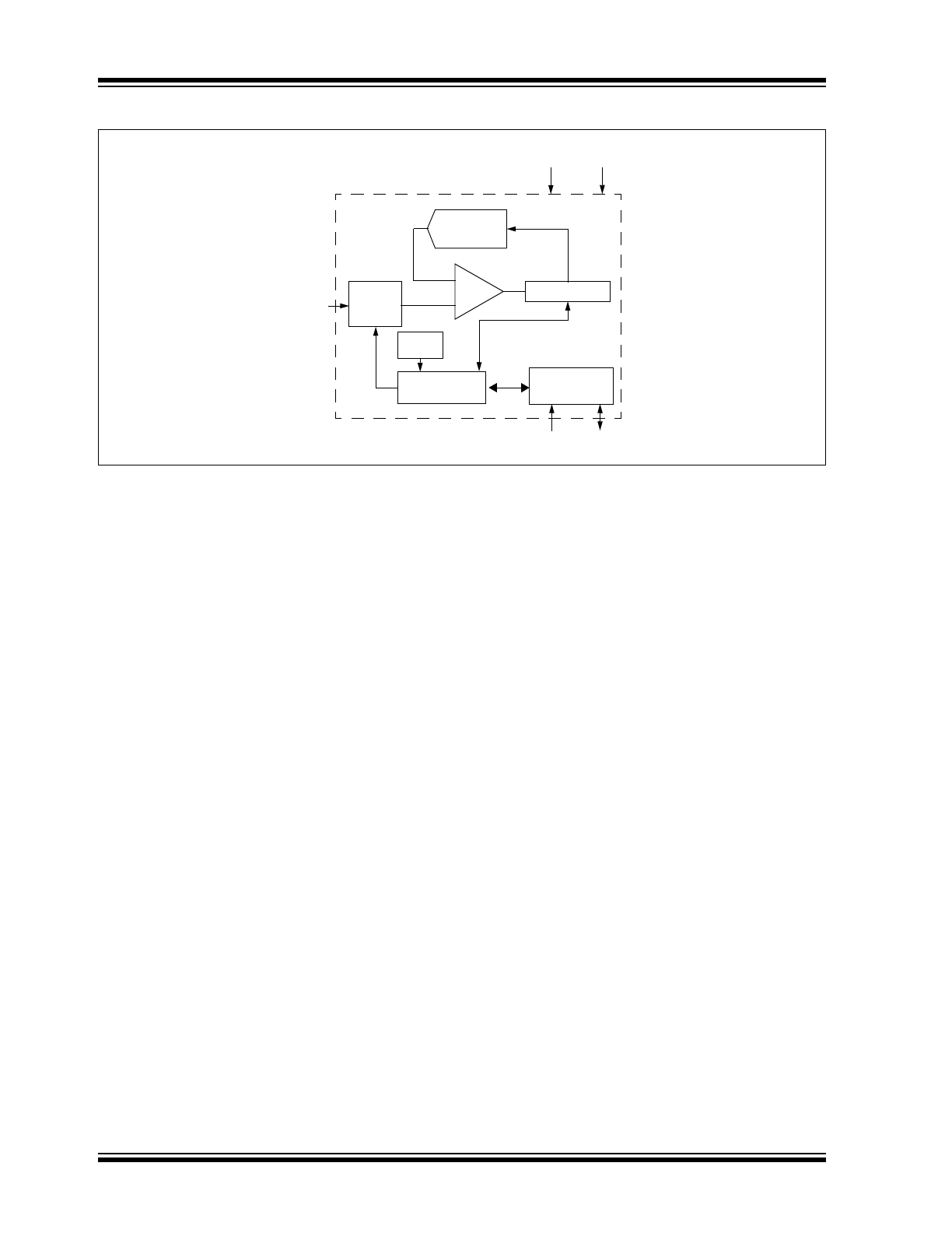
Functional Block Diagram
Comparator
10-bit SAR
DAC
A
IN
V
SS
V
DD
SCL
SDA
Clock
Control Logic
–
+
Sample
and
Hold
I
2
C
Interface
2003-2017 Microchip Technology Inc.
DS20001805C-page 3
MCP3021
1.0
ELECTRICAL CHARACTERISTICS
Absolute Maximum Ratings †
V
DD
...........................................................................................................................................................................+7.0V
Analog input pin w.r.t. V
SS
..................................................................................................................-0.6V to V
DD
+0.6V
SDA and SCL pins w.r.t. V
SS
...............................................................................................................-0.6V to V
DD
+1.0V
Storage Temperature ............................................................................................................................. -65°C to +150°C
Ambient Temperature with power applied ...............................................................................................-65°C to +125°C
Maximum Junction Temperature ........................................................................................................................... +150°C
ESD protection on all pins (HBM) .......................................................................................................................... ≥ 4 kV
† Notice: Stresses above those listed under “Absolute Maximum Ratings” may cause permanent damage to the
device. This is a stress rating only and functional operation of the device at those or any other conditions above those
indicated in the operational listings of this specification is not intended. Exposure to maximum rating conditions for
extended periods may affect device reliability.
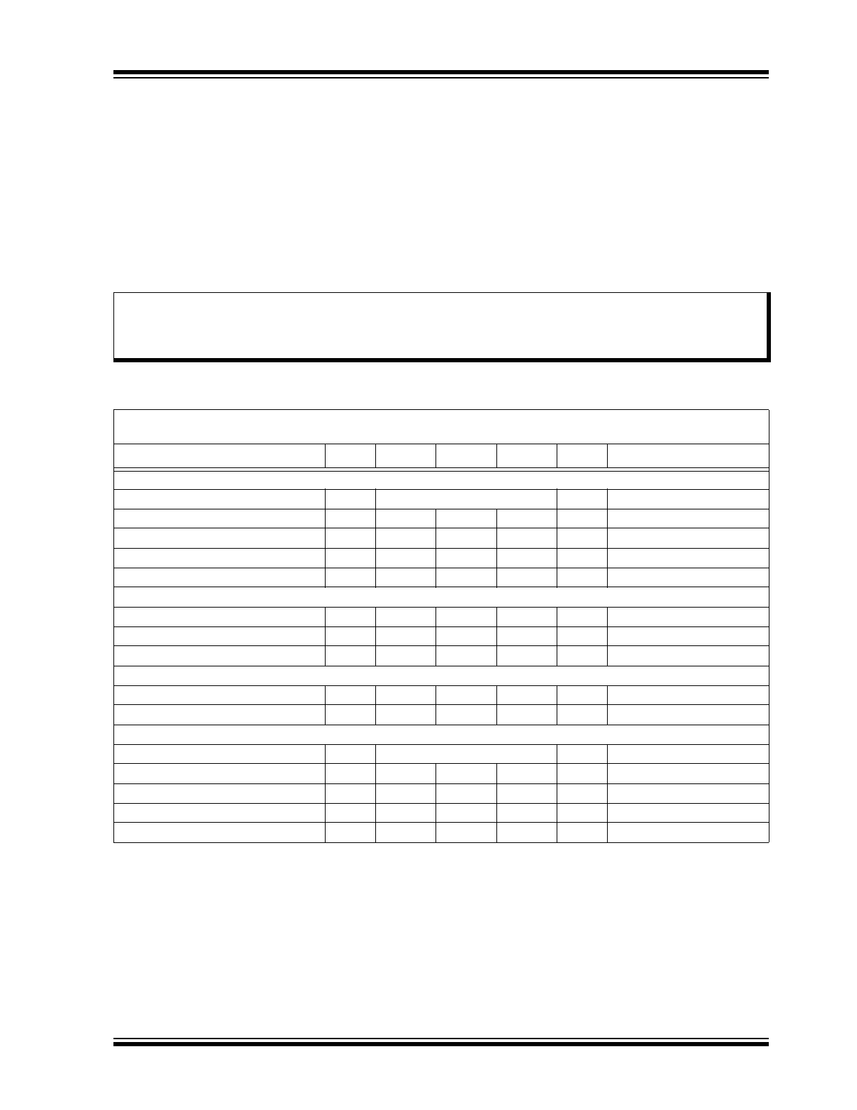
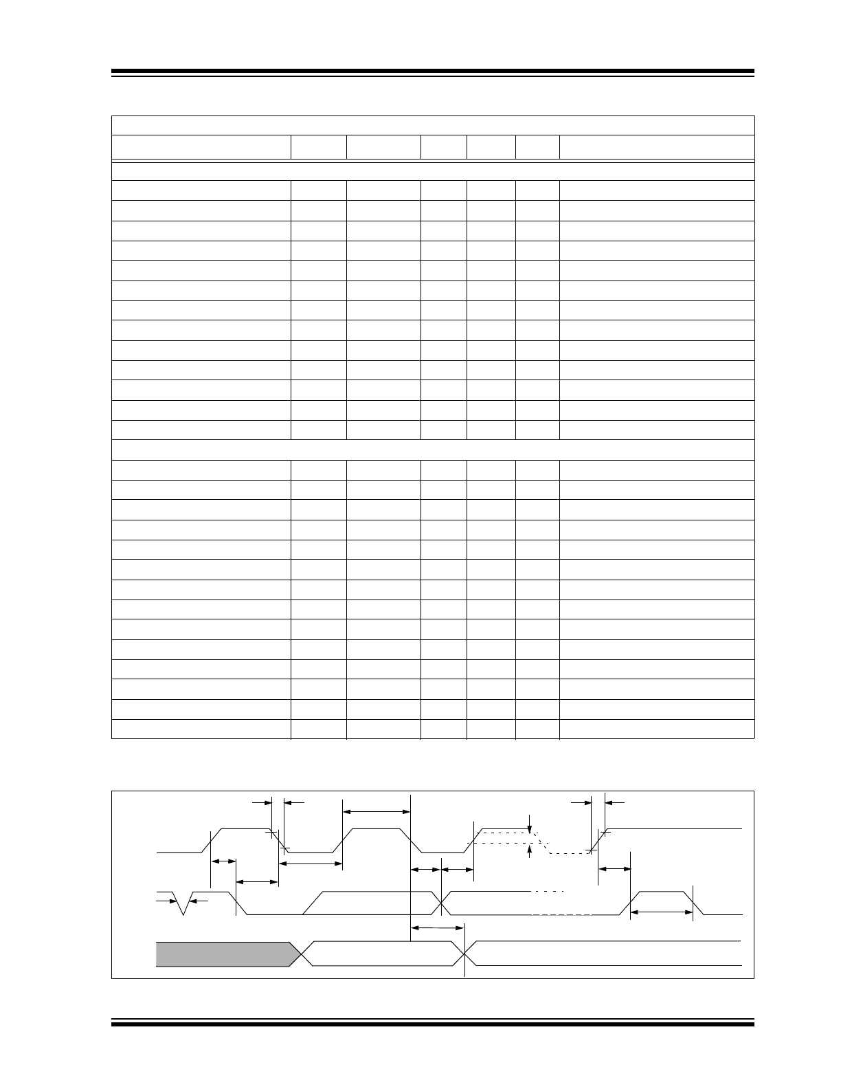
DC ELECTRICAL SPECIFICATIONS
Electrical Characteristics: Unless otherwise noted, all parameters apply at V
DD
= 5.0V, V
SS
= GND, R
PU
= 2 k
T
A
= -40°C to +85°C, I
2
C Fast Mode Timing: f
SCL
= 400 kHz (
Note 3
).
Parameter
Sym.
Min.
Typ.
Max.
Units
Conditions
DC Accuracy
Resolution
—
10
bits
Integral Nonlinearity
INL
—
±0.25
±1
LSB
Differential Nonlinearity
DNL
—
±0.25
±1
LSB
No missing codes
Offset Error
—
—
±0.75
±3
LSB
Gain Error
—
—
-1
±3
LSB
Dynamic Performance
Total Harmonic Distortion
THD
—
-70
—
dB
V
IN
= 0.1V to 4.9V @ 1 kHz
Signal-to-Noise and Distortion
SINAD
—
60
—
dB
V
IN
= 0.1V to 4.9V @ 1 kHz
Spurious Free Dynamic Range
SFDR
—
74
—
dB
V
IN
= 0.1V to 4.9V @ 1 kHz
Analog Input
Input Voltage Range
—
V
SS
-0.3
—
V
DD
+0.3
V
2.7V
V
DD
5.5V
Leakage Current
—
-1
—
+1
µA
SDA/SCL (open-drain output)
Data Coding Format
—
Straight Binary
—
High-Level Input Voltage
V
IH
0.7 V
DD
—
—
V
Low-Level Input Voltage
V
IL
—
—
0.3 V
DD
V
Low-Level Output Voltage
V
OL
—
—
0.4
V
I
OL
= 3 mA, R
PU
= 1.53 k
Hysteresis of Schmitt Trigger Inputs
V
HYST
—
0.05V
DD
—
V
f
SCL
= 400 kHz only
Note 1: Sample time is the time between conversions after the address byte has been sent to the converter. Refer
to
Figure 5-6
.
2: This parameter is periodically sampled and not 100% tested.
3: R
PU
= Pull-up resistor on SDA and SCL.
4: SDA and SCL = V
SS
to V
DD
at 400 kHz.
5: t
ACQ
and t
CONV
are dependent on internal oscillator timing. See
Figure 5-5
and
Figure 5-6
in relation to
SCL.
MCP3021
DS20001805C-page 4
2003-2017 Microchip Technology Inc.
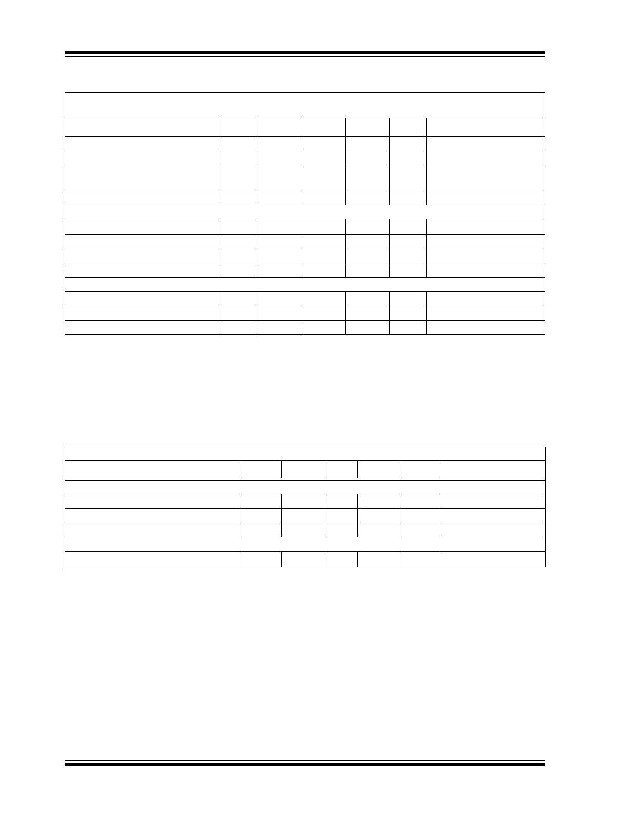
TEMPERATURE SPECIFICATIONS
Input Leakage Current
I
LI
-1
—
+1
µA
V
IN
= V
SS
to V
DD
Output Leakage Current
I
LO
-1
—
+1
µA
V
OUT
= V
SS
to V
DD
Pin Capacitance
(all inputs/outputs)
C
IN
,
C
OUT
—
—
10
pF
T
A
= 25°C, f = 1 MHz;
(
Note 2
)
Bus Capacitance
C
B
—
—
400
pF
SDA drive low, 0.4V
Power Requirements
Operating Voltage
V
DD
2.7
—
5.5
V
Conversion Current
I
DD
—
175
250
µA
Standby Current
I
DDS
—
0.005
1
µA
SDA, SCL = V
DD
Active Bus Current
I
DDA
—
—
120
µA
Note 4
Conversion Rate
Conversion Time
t
CONV
—
8.96
—
µs
Note 5
Analog Input Acquisition Time
t
ACQ
—
1.12
—
µs
Note 5
Sample Rate
f
SAMP
—
—
22.3
ksps
f
SCL
= 400 kHz (
Note 1
)
Electrical Characteristics: Unless otherwise noted, all parameters apply at V
DD
= 5.0V, V
SS
= GND.
Parameter
Sym.
Min.
Typ.
Max.
Units
Conditions
Temperature Ranges
Operating Temperature Range
T
A
-40
—
+125
°C
Extended Temperature Range
T
A
-40
—
+125
°C
Storage Temperature Range
T
A
-65
—
+150
°C
Thermal Package Resistances
Thermal Resistance, SOT-23
JA
—
256
—
°C/W
DC ELECTRICAL SPECIFICATIONS (CONTINUED)
Electrical Characteristics: Unless otherwise noted, all parameters apply at V
DD
= 5.0V, V
SS
= GND, R
PU
= 2 k
T
A
= -40°C to +85°C, I
2
C Fast Mode Timing: f
SCL
= 400 kHz (
Note 3
).
Parameter
Sym.
Min.
Typ.
Max.
Units
Conditions
Note 1: Sample time is the time between conversions after the address byte has been sent to the converter. Refer
to
Figure 5-6
.
2: This parameter is periodically sampled and not 100% tested.
3: R
PU
= Pull-up resistor on SDA and SCL.
4: SDA and SCL = V
SS
to V
DD
at 400 kHz.
5: t
ACQ
and t
CONV
are dependent on internal oscillator timing. See
Figure 5-5
and
Figure 5-6
in relation to
SCL.
2003-2017 Microchip Technology Inc.
DS20001805C-page 5
MCP3021
TIMING SPECIFICATIONS
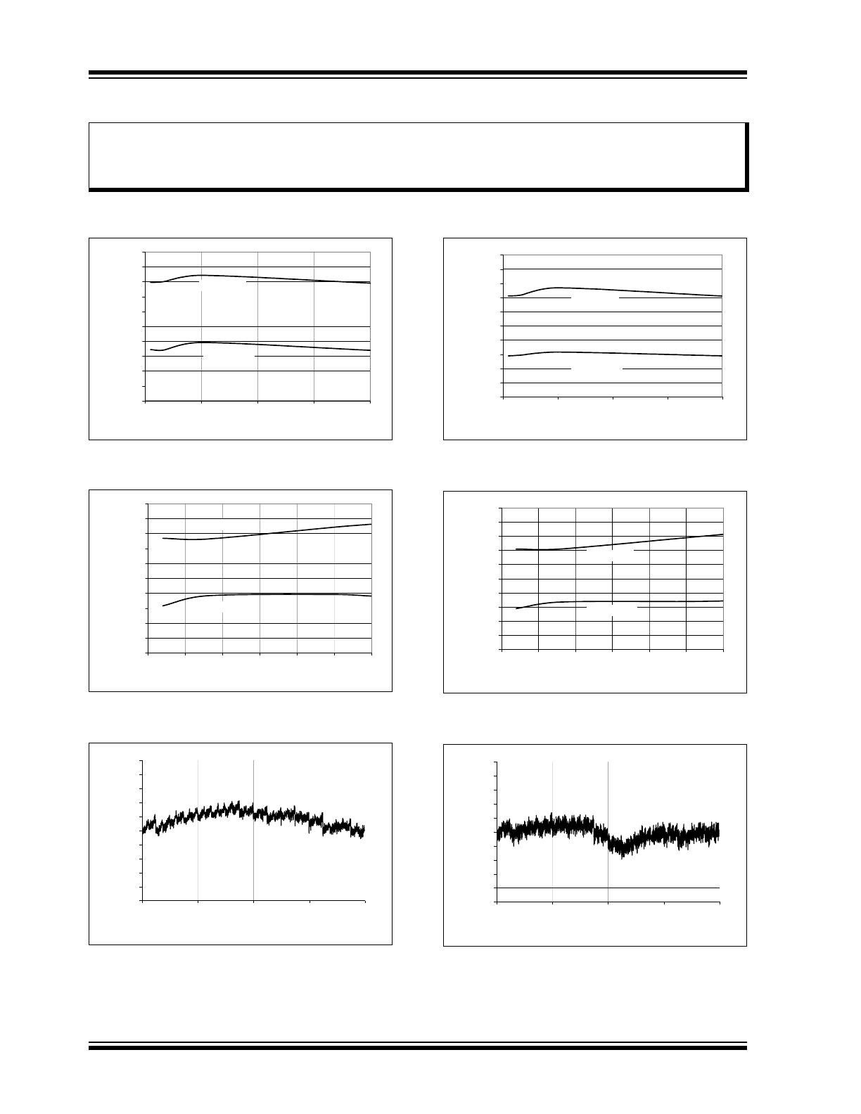
FIGURE 1-1:
Standard and Fast Mode Bus Timing Data.
Electrical Characteristics: All parameters apply at V
DD
= 2.7V - 5.5V, V
SS
= GND, T
A
= -40°C to +85°C.
Parameter
Sym.
Min.
Typ.
Max.
Units
Conditions
I
2
C Standard Mode
Clock Frequency
f
SCL
0
—
100
kHz
Clock High Time
T
HIGH
4000
—
—
ns
Clock Low Time
T
LOW
4700
—
—
ns
SDA and SCL Rise Time
T
R
—
—
1000
ns
From V
IL
to V
IH
(
Note 1
)
SDA and SCL Fall Time
T
F
—
—
300
ns
From V
IL
to V
IH
(
Note 1
)
Start Condition Hold Time
T
HD:STA
4000
—
—
ns
Start Condition Setup Time
T
SU:STA
4700
—
—
ns
Data Input Setup Time
T
SU:DAT
250
—
—
ns
Stop Condition Setup Time
T
SU:STO
4000
—
—
ns
Stop Condition Hold Time
T
HD:STD
4000
—
—
ns
Output Valid from Clock
T
AA
—
—
3500
ns
Bus Free Time
T
BUF
4700
—
—
ns
Note 2
Input Filter Spike Suppression
T
SP
—
—
50
ns
SDA and SCL pins (
Note 1
)
I
2
C Fast Mode
Clock Frequency
F
SCL
0
—
400
kHz
Clock High Time
T
HIGH
600
—
—
ns
Clock Low Time
T
LOW
1300
—
—
ns
SDA and SCL Rise Time
T
R
20 + 0.1C
B
—
300
ns
From V
IL
to V
IH
(
Note 1
)
SDA and SCL Fall Time
T
F
20 + 0.1C
B
—
300
ns
From V
IL
to V
IH
(
Note 1
)
Start Condition Hold Time
T
HD:STA
600
—
—
ns
Start Condition Setup time
T
SU:STA
600
—
—
ns
Data Input Hold Time
T
HD:DAT
0
—
0.9
ms
Data Input Setup Time
T
SU:DAT
100
—
—
ns
Stop Condition Setup Time
T
SU:STO
600
—
—
ns
Stop Condition Hold Time
T
HD:STD
600
—
—
ns
Output Valid from Clock
T
AA
—
—
900
ns
Bus Free Time
T
BUF
1300
—
—
ns
Note 2
Input Filter Spike Suppression
T
SP
—
—
50
ns
SDA and SCL pins (
Note 1
)
Note 1: This parameter is periodically sampled and not 100% tested.
2: Time the bus must be free before a new transmission can start.
T
F
T
HIGH
V
HYS
T
R
T
SU:STA
T
SP
T
HD:STA
T
LOW
T
HD:DAT
T
SU:DAT
T
SU:STO
T
BUF
T
AA
SCL
SDA
IN
SDA
OUT
MCP3021
DS20001805C-page 6
2003-2017 Microchip Technology Inc.
2.0
TYPICAL PERFORMANCE CURVES
Note: Unless otherwise indicated, V
DD
= 5V, V
SS
= 0V, I
2
C Fast Mode Timing (SCL = 400 kHz), Continuous Conversion
Mode (f
SAMP
= 22.3 ksps), T
A
= +25°C.
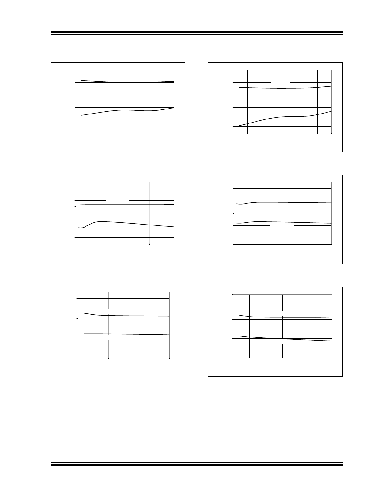
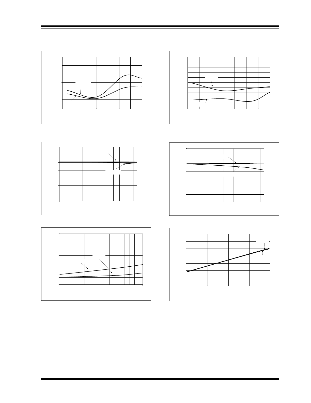
FIGURE 2-1:
INL vs. Clock Rate.
FIGURE 2-2:
INL vs. V
DD
- I
2
C Standard
Mode (f
SCL
= 100 kHz).
FIGURE 2-3:
INL vs. Code
(Representative Part).
FIGURE 2-4:
INL vs. Clock Rate
(V
DD
= 2.7V).
FIGURE 2-5:
INL vs. V
DD
- I
2
C Fast Mode
(f
SCL
= 400 kHz).
FIGURE 2-6:
INL vs. Code
(Representative Part, V
DD
= 2.7V).
Note:
The graphs and tables provided following this note are a statistical summary based on a limited number of
samples and are provided for informational purposes only. The performance characteristics listed herein
are not tested or guaranteed. In some graphs or tables, the data presented may be outside the specified
operating range (e.g., outside specified power supply range) and therefore outside the warranted range.
-1
-0.8
-0.6
-0.4
-0.2
0
0.2
0.4
0.6
0.8
1
0
100
200
300
400
I
2
C Bus Rate (kHz)
INL
(
L
SB)
Positive INL
Negative INL
0.25
0.20
0.15
0.10
0.005
-0.005
-0.10
-0.15
-0.20
-0.25
-1
-0.8
-0.6
-0.4
-0.2
0
0.2
0.4
0.6
0.8
1
2.5
3
3.5
4
4.5
5
5.5
V
DD
(V)
INL (LSB)
Positive INL
Negative INL
0.25
0.20
0.15
0.10
0.005
-0.005
-0.10
-0.15
-0.20
-0.25
-0.5
-0.4
-0.3
-0.2
-0.1
0
0.1
0.2
0.3
0.4
0.5
0
256
512
768
1024
Digital Code
INL (LSB)
-1
-0.8
-0.6
-0.4
-0.2
0
0.2
0.4
0.6
0.8
1
0
100
200
300
400
I
2
C Bus Rate (kHz)
INL (LSB)
Positive INL
Negative INL
0.25
0.20
0.15
0.10
0.005
-0.005
-0.10
-0.15
-0.20
-0.25
-1
-0.8
-0.6
-0.4
-0.2
0
0.2
0.4
0.6
0.8
1
2.5
3
3.5
4
4.5
5
5.5
V
DD
(V)
INL
(
L
SB)
Positive INL
Negative INL
0.25
0.20
0.15
0.10
0.005
-0.005
-0.10
-0.15
-0.20
-0.25
-0.5
-0.4
-0.3
-0.2
-0.1
0
0.1
0.2
0.3
0.4
0.5
0
256
512
768
1024
Digital Code
INL (LSB)
2003-2017 Microchip Technology Inc.
DS20001805C-page 7
MCP3021
Note: Unless otherwise indicated, V
DD
= 5V, V
SS
= 0V, I
2
C Fast Mode Timing (SCL = 400 kHz), Continuous Conversion
Mode (f
SAMP
= 22.3 ksps), T
A
= +25°C.
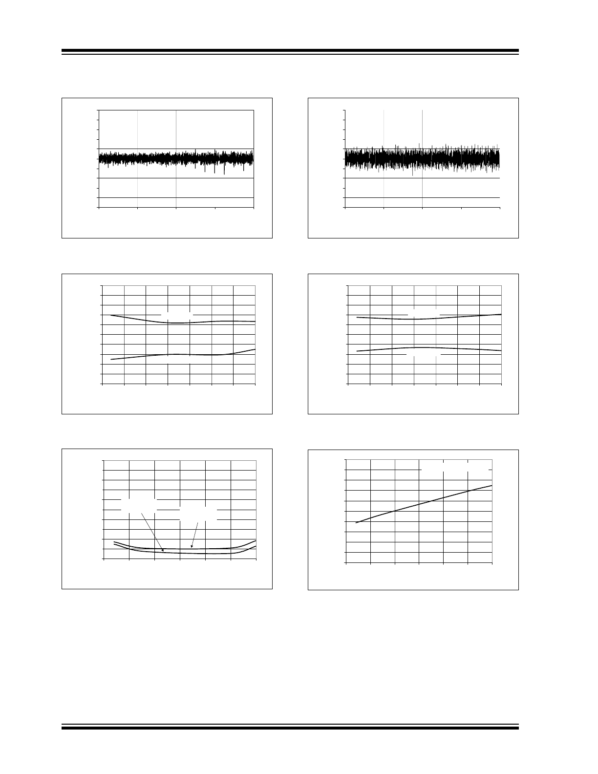
FIGURE 2-7:
INL vs. Temperature.
FIGURE 2-8:
DNL vs. Clock Rate.
FIGURE 2-9:
DNL vs. V
DD
- I
2
C Standard
Mode (f
SCL
= 100 kHz).
FIGURE 2-10:
INL vs. Temperature
(V
DD
= 2.7V).
FIGURE 2-11:
DNL vs. Clock Rate
(V
DD
= 2.7V).
FIGURE 2-12:
DNL vs. V
DD
- I
2
C Fast
Mode (f
SCL
= 400 kHz).
-1
-0.8
-0.6
-0.4
-0.2
0
0.2
0.4
0.6
0.8
1
-50
-25
0
25
50
75
100
125
Temperature (°C)
IN
L
(L
SB
)
Positive INL
Negative INL
0.25
0.20
0.15
0.10
0.005
-0.005
-0.10
-0.15
-0.20
-0.25
-1
-0.8
-0.6
-0.4
-0.2
0
0.2
0.4
0.6
0.8
1
0
100
200
300
400
I
2
C Bus Rate (kHz)
DNL
(L
SB)
Positive DNL
Negative DNL
0.25
0.20
0.15
0.10
0.005
-0.005
-0.10
-0.15
-0.20
-0.25
-1
-0.8
-0.6
-0.4
-0.2
0
0.2
0.4
0.6
0.8
1
2.5
3
3.5
4
4.5
5
5.5
V
DD
(V)
DNL (LSB)
Positive DNL
Negative DNL
0.25
0.20
0.15
0.10
0.005
-0.005
-0.10
-0.15
-0.20
-0.25
-1
-0.8
-0.6
-0.4
-0.2
0
0.2
0.4
0.6
0.8
1
-50
-25
0
25
50
75
100
125
Temperature (°C)
INL
(
L
SB)
Negative INL
Positive INL
0.25
0.20
0.15
0.10
0.005
-0.005
-0.10
-0.15
-0.20
-0.25
-1
-0.8
-0.6
-0.4
-0.2
0
0.2
0.4
0.6
0.8
1
0
100
200
300
400
I
2
C Bus Rate (kHz)
DNL
(
L
SB)
Negative DNL
Positive DNL
0.25
0.20
0.15
0.10
0.005
-0.005
-0.10
-0.15
-0.20
-0.25
-1
-0.8
-0.6
-0.4
-0.2
0
0.2
0.4
0.6
0.8
1
2.5
3
3.5
4
4.5
5
5.5
V
DD
(V)
DNL (LSB)
Positive DNL
Negative DNL
0.25
0.20
0.15
0.10
0.005
-0.005
-0.10
-0.15
-0.20
-0.25
MCP3021
DS20001805C-page 8
2003-2017 Microchip Technology Inc.
Note: Unless otherwise indicated, V
DD
= 5V, V
SS
= 0V, I
2
C Fast Mode Timing (SCL = 400 kHz), Continuous Conversion
Mode (f
SAMP
= 22.3 ksps), T
A
= +25°C.
FIGURE 2-13:
DNL vs. Code
(Representative Part).
FIGURE 2-14:
DNL vs. Temperature.
FIGURE 2-15:
Gain Error vs. V
DD
.
FIGURE 2-16:
DNL vs. Code
(Representative Part, V
DD
= 2.7V).
FIGURE 2-17:
DNL vs. Temperature
(V
DD
= 2.7V).
FIGURE 2-18:
Offset Error vs. V
DD
.
-0.5
-0.4
-0.3
-0.2
-0.1
0
0.1
0.2
0.3
0.4
0.5
0
256
512
768
1024
Digital Code
DNL (LSB)
-1
-0.8
-0.6
-0.4
-0.2
0
0.2
0.4
0.6
0.8
1
-50
-25
0
25
50
75
100
125
Temperature (°C)
DNL
(
L
SB)
Negative DNL
Positive DNL
0.25
0.20
0.15
0.10
0.005
-0.005
-0.10
-0.15
-0.20
-0.25
-1
-0.9
-0.8
-0.7
-0.6
-0.5
-0.4
-0.3
-0.2
-0.1
0
2.5
3
3.5
4
4.5
5
5.5
V
DD
(V)
Ga
in Error (LSB)
Fast Mode
(f
SCL
=100 kHz)
Standard Mode
(f
SCL
=400 kHz)
0
-0.025
-0.05
-0.075
-0.1
-0.15
-0.175
-0.2
-0.225
-0.25
-0.125
-0.5
-0.4
-0.3
-0.2
-0.1
0
0.1
0.2
0.3
0.4
0.5
0
256
512
768
1024
Digital Code
DNL (LSB)
-1
-0.8
-0.6
-0.4
-0.2
0
0.2
0.4
0.6
0.8
1
-50
-25
0
25
50
75
100
125
Temperature (°C)
DNL
(
L
SB)
Positive DNL
Negative DNL
0.25
0.20
0.15
0.10
0.005
-0.005
-0.10
-0.15
-0.20
-0.25
0
0.1
0.2
0.3
0.4
0.5
0.6
0.7
0.8
0.9
1
2.5
3
3.5
4
4.5
5
5.5
V
DD
(V)
O
ff
set
Error (
L
SB)
f
SCL
= 100 kHz & 400 kHz
0.25
0.225
0.2
0.175
0.15
0.1
0.075
0.05
0.025
0
0.125
2003-2017 Microchip Technology Inc.
DS20001805C-page 9
MCP3021
Note: Unless otherwise indicated, V
DD
= 5V, V
SS
= 0V, I
2
C Fast Mode Timing (SCL = 400 kHz), Continuous Conversion
Mode (f
SAMP
= 22.3 ksps), T
A
= +25°C.
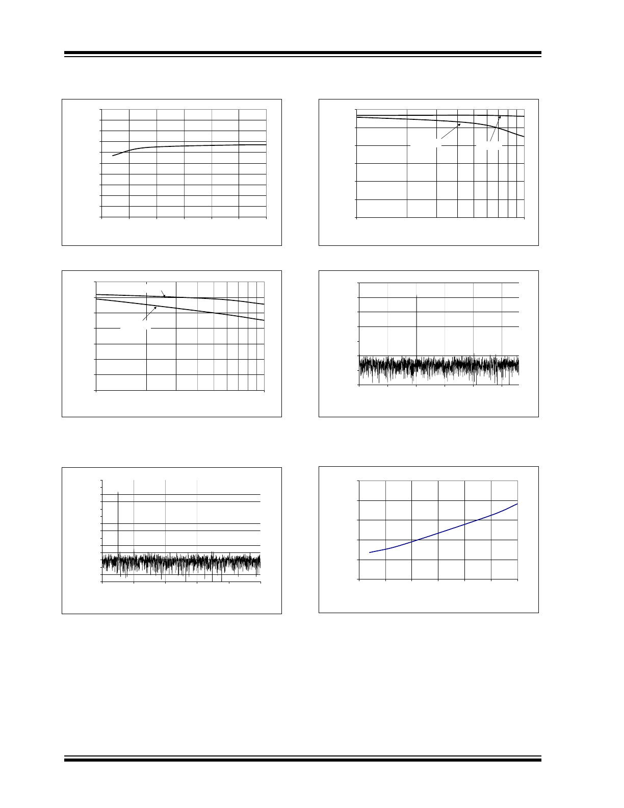
FIGURE 2-19:
Gain Error vs. Temperature.
FIGURE 2-20:
SNR vs. Input Frequency.
FIGURE 2-21:
THD vs. Input Frequency.
FIGURE 2-22:
Offset Error vs.
Temperature.
FIGURE 2-23:
SINAD vs. Input Frequency.
FIGURE 2-24:
SINAD vs. Input Signal
Level.
-1.5
-1
-0.5
0
0.5
1
1.5
-50
-25
0
25
50
75
100
125
Temperature (°C)
G
ain Error (
L
SB)
V
DD
= 5V
V
DD
= 2.7V
0.375
0.250
0.125
-0.125
-0.250
-0.375
12
24
36
48
60
72
84
96
1
10
Input Frequency (kHz)
SNR (dB)
V
DD
= 5V
V
DD
= 2.7V
Y
84
72
60
48
36
24
12
0
-96
-84
-72
-60
-48
-36
-24
-12
1
10
Input Frequency (kHz)
THD (dB)
V
DD
= 2.7V
V
DD
= 5V
0
-12
-24
-36
-48
-60
-72
-84
0
0.2
0.4
0.6
0.8
1
1.2
1.4
1.6
1.8
2
-50
-25
0
25
50
75
100
125
Temperature (°C)
O
ff
set
Error (
L
SB)
V
DD
= 5V
V
DD
= 2.7V
0.50
0.45
0.40
0.35
0.30
0.25
0.15
0.10
0.05
0
0.20
12
24
36
48
60
72
84
96
1
10
Input Frequency (kHz)
SINAD (dB)
V
DD
= 5V
V
DD
= 2.7V
84
72
60
48
36
24
12
0
12
24
36
48
60
72
84
96
-40
-30
-20
-10
0
Input Signal Level (dB)
SINAD (dB)
V
DD
= 5V
V
DD
= 2.7V
84
72
60
48
36
24
12
0
MCP3021
DS20001805C-page 10
2003-2017 Microchip Technology Inc.
Note: Unless otherwise indicated, V
DD
= 5V, V
SS
= 0V, I
2
C Fast Mode Timing (SCL = 400 kHz), Continuous Conversion
Mode (f
SAMP
= 22.3 ksps), T
A
= +25°C.
FIGURE 2-25:
ENOB vs. V
DD
.
FIGURE 2-26:
SFDR vs. Input Frequency.
FIGURE 2-27:
Spectrum Using I
2
C Fast
Mode (Representative Part, 1 kHz Input
Frequency).
FIGURE 2-28:
ENOB vs. Input Frequency.
FIGURE 2-29:
Spectrum Using I
2
C
Standard Mode (Representative Part, 1 kHz
Input Frequency).
FIGURE 2-30:
I
DD
(Conversion) vs. V
DD
.
11.5
11.55
11.6
11.65
11.7
11.75
11.8
11.85
11.9
11.95
12
2.5
3
3.5
4
4.5
5
5.5
V
DD
(V)
ENO
B
(
rm
s)
10
9.95
9.90
9.85
9.80
9.75
9.70
9.65
9.60
9.55
9.50
12
24
36
48
60
72
84
96
1
10
Input Frequency (kHz)
SFDR (dB)
V
DD
= 2.7V
V
DD
= 5 V
84
72
60
48
36
24
12
0
-130
-120
-110
-100
-90
-80
-70
-60
-50
-40
-30
-20
-10
0
10
0
2000
4000
6000
8000
10000
Frequency (Hz)
Amplitude (dB)
9
9.5
10
10.5
11
11.5
12
1
10
Input Frequency (kHz)
ENO
B
(
rm
s)
V
DD
= 2.7V
V
DD
= 5V
10
9.5
9.0
8.5
8.0
7.7
7.0
-130
-110
-90
-70
-50
-30
-10
10
0
500
1000
1500
2000
2500
Frequency (Hz)
Amplitude (dB)
0
50
100
150
200
250
2.5
3
3.5
4
4.5
5
5.5
V
DD
(V)
I
DD
(µA
)
