

2014-2017 Microchip Technology Inc.
DS20005282B-page 1
MCP25625
General Features
• Stand-Alone CAN 2.0B Controller with Integrated
CAN Transceiver and Serial Peripheral
Interface (SPI)
• Up to 1 Mb/s Operation
• Very Low Standby Current (10 µA, typical)
• Up to 10 MHz SPI Clock Speed
• Interfaces Directly with Microcontrollers with 2.7V
to 5.5V I/Os
• Available in SSOP-28L and 6x6 QFN-28L
• Temperature Ranges:
- Extended (E): -40°C to +125°C
CAN Controller Features
• V
DD
: 2.7 to 5.5V
• Implements CAN 2.0B (ISO11898-1)
• Three Transmit Buffers with Prioritization and
Abort Features
• Two Receive Buffers
• Six Filters and Two Masks with Optional Filtering
on the First Two Data Bytes
• Supports SPI Modes 0,0 and 1,1
• Specific SPI Commands to Reduce SPI Overhead
• Buffer Full and Request-to-Send Pins are
Configurable as General Purpose I/Os
• One Interrupt Output Pin
CAN Transceiver Features
• V
DDA
: 4.5V to 5.5V
• Implements ISO-11898-2 and ISO-11898-5
Standard Physical Layer Requirements
• CAN Bus Pins are Disconnected when Device is
Unpowered:
- An unpowered node or brown-out event will
not load the CAN bus
• Detection of Ground Fault:
- Permanent Dominant detection on T
XD
- Permanent Dominant detection on bus
• Power-on Reset and Voltage Brown-Out
Protection on V
DDA
Pin
• Protection Against Damage Due to Short-Circuit
Conditions (Positive or Negative Battery Voltage)
• Protection Against High-Voltage Transients in
Automotive Environments
• Automatic Thermal Shutdown Protection
• Suitable for 12V and 24V Systems
• Meets or Exceeds Stringent Automotive Design
Requirements, Including “Hardware Require-
ments for LIN, CAN and FlexRay Interfaces in
Automotive Applications”, Version 1.3, May 2012
• High Noise Immunity Due to Differential Bus
Implementation
• High-ESD Protection on CANH and CANL, Meets
IEC61000-4-2 up to ±8 kV
Description
The MCP25625 is a complete, cost-effective and small
footprint CAN solution that can be easily added to a
microcontroller with an available SPI interface.
The MCP25625 interfaces directly with microcontrollers
operating at 2.7V to 5.5V; there are no external level
shifters required. In addition, the MCP25625 connects
directly to the physical CAN bus, supporting all
requirements for CAN high-speed transceivers.
The MCP25625 meets the automotive requirements for
high-speed (up to 1 Mb/s), low quiescent current,
Electromagnetic Compatibility (EMC) and Electrostatic
Discharge (ESD).
CAN Controller with Integrated Transceiver
MCP25625
DS20005282B-page 2
2014-2017 Microchip Technology Inc.
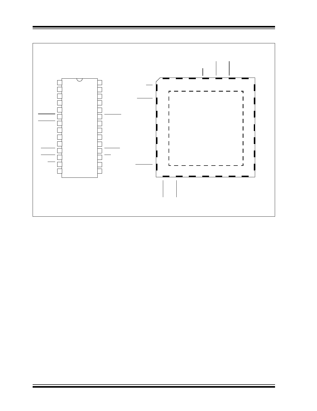
Package Types
V
DD
TxCAN
Tx
2R
T
S
V
IO
R
XD
RESET
CS
RxCAN
CLKOUT
CANH
SO
Tx
1R
T
S
NC
STBY
T
XD
NC
V
SS
V
DDA
OSC2
SCK
IN
T
Rx0
B
F
Rx1
B
F
GND
Tx0RTS
CANL
OSC1
SI
1
2
3
4
5
6
7
15
8
9
10
11
12
13
14
16
17
18
19
20
21
26
25
24
23
22
28
27
EXP-29
28
16
27
26
25
24
23
22
21
20
19
18
17
15
1
13
2
3
4
5
6
7
8
9
10
11
12
14
V
IO
GND
Rx1BF
Rx0BF
INT
SCK
CANL
NC
CANH
STBY
Tx1RTS
Tx2RTS
OSC2
OSC1
R
XD
V
DD
RESET
CS
SO
SI
V
SS
V
DDA
NC
T
XD
Tx0RTS
CLKOUT
RxCAN
TxCAN
MCP25625
6x6 QFN
*
MCP25625
SSOP
*
Includes Exposed Thermal Pad (EP); see
Table 1-1
.
2014-2017 Microchip Technology Inc.
DS20005282B-page 3
MCP25625
1.0
DEVICE OVERVIEW
A typical CAN solution consists of a CAN controller that
implements the CAN protocol, and a CAN transceiver
that serves as the interface to the physical CAN bus.
The MCP25625 integrates both the CAN controller and
the CAN transceiver. Therefore, it is a complete CAN
solution that can be easily added to a microcontroller
with an SPI interface.
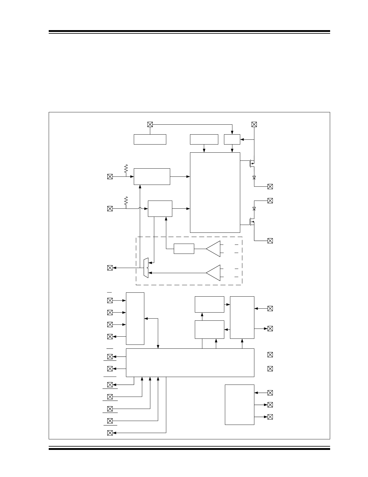
1.1
Block Diagram
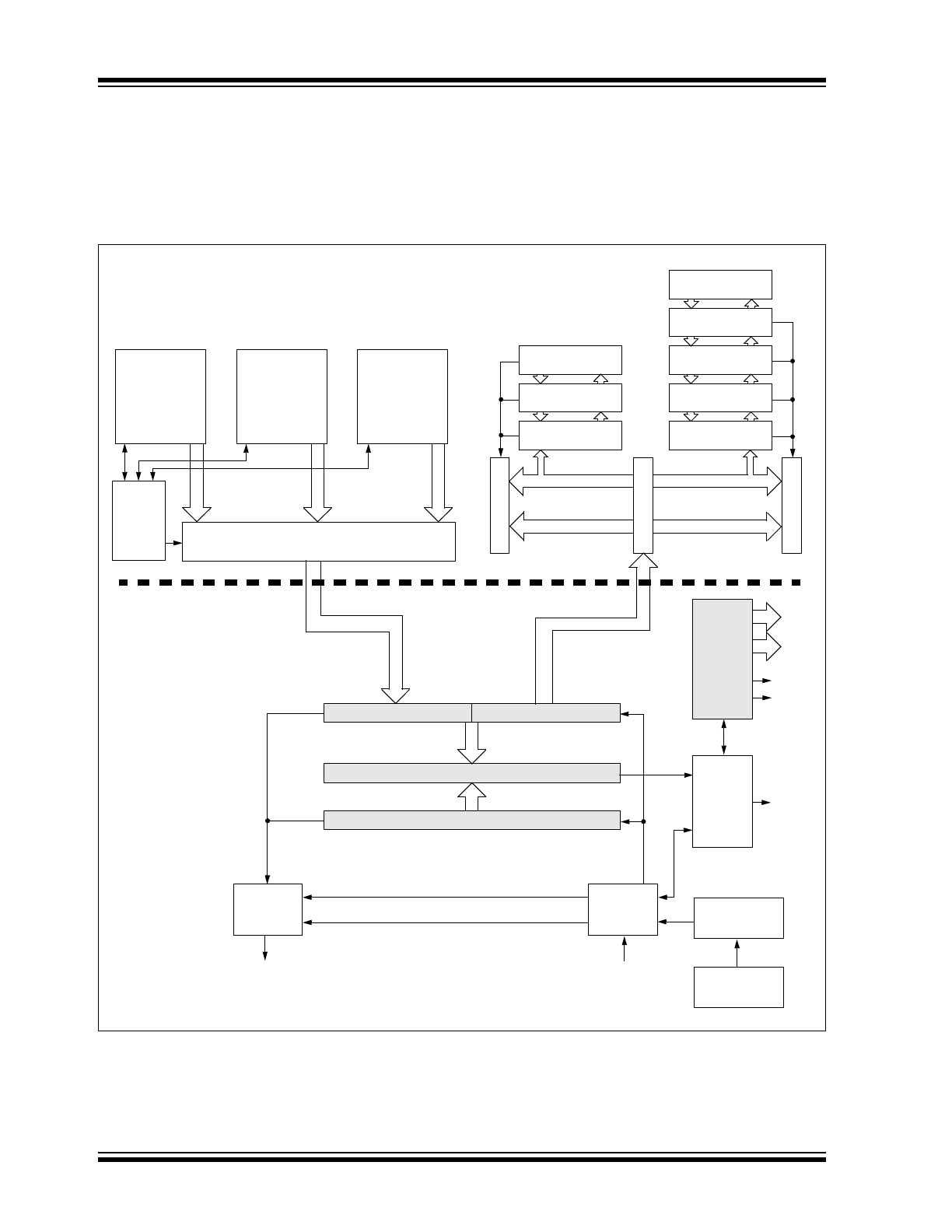
Figure 1-1
shows the block diagram of the MCP25625.
The CAN transceiver is illustrated in the top half of the
block diagram, see
Section 6.0 “CAN Transceiver”
for more details.
The CAN controller is depicted at the bottom half of the
block diagram, and described in more detail in
Section 3.0 “CAN Controller”
.
FIGURE 1-1:
MCP25625 BLOCK DIAGRAM
V
DDA
CANH
CANL
T
XD
R
XD
Driver
and
Slope Control
Thermal
Protection
POR
UVLO
Digital I/O
Supply
V
IO
V
SS
STBY
Permanent
Dominant Detect
V
IO
V
IO
Mode
Control
Wake-up
Filter
CANH
CANL
CANH
CANL
Receiver
LP_R
X
HS_R
X
SPI IF
CAN
Protocol
Engine
Tx Handler
Tx
Prioritization
Control Logic
Registers: Configuration, Control and Interrupts
Rx Handler
Acceptance
Filters and
Masks
TxCAN
RxCAN
CS
SCK
SI
SO
OSC1
OSC2
CLKOUT
INT
Rx0BF
RESET
Crystal
Oscillator
Rx1BF
Tx0RTS
Tx1RTS
Tx2RTS
V
DD
GND

MCP25625
DS20005282B-page 4
2014-2017 Microchip Technology Inc.
1.2
Pin Out Description
The descriptions of the pins are listed in
Table 1-1
.
TABLE 1-1:
MCP25625 PIN DESCRIPTION
Pin Name
6x6
QFN
SSOP
Block
(
1
)
Pin Type
Description
V
IO
11
1
CAN Transceiver
P
Digital I/O Supply Pin for CAN Transceiver
NC
14
2
—
—
No Connection
CANL
12
3
CAN Transceiver
HV I/O
CAN Low-Level Voltage I/O
CANH
13
4
CAN Transceiver
HV I/O
CAN High-Level Voltage I/O
STBY
15
5
CAN Transceiver
I
Standby Mode Input
Tx1RTS
8
6
CAN Controller
I
TXB1 Request-to-Send
Tx2RTS
9
7
CAN Controller
I
TXB2 Request-to-Send
OSC2
20
8
CAN Controller
O
External Oscillator Output
OSC1
21
9
CAN Controller
I
External Oscillator Input
GND
22
10
CAN Controller
P
Ground
Rx1BF
23
11
CAN Controller
O
RxB1 Interrupt
Rx0BF
24
12
CAN Controller
O
RxB0 Interrupt
INT
25
13
CAN Controller
O
Interrupt Output
SCK
26
14
CAN Controller
I
SPI Clock Input
SI
27
15
CAN Controller
I
SPI Data Input
SO
28
16
CAN Controller
O
SPI Data Output
CS
1
17
CAN Controller
I
SPI Chip Select Input
RESET
2
18
CAN Controller
I
Reset Input
V
DD
3
19
CAN Controller
P
Power for CAN Controller
TxCAN
4
20
CAN Controller
O
Transmit Output to CAN Transceiver
R
X
CAN
5
21
CAN Controller
I
Receive Input from CAN Transceiver
CLKOUT
6
22
CAN Controller
O
Clock Output/SOF
Tx0RTS
7
23
CAN Controller
I
TXB0 Request-to-Send
T
XD
16
24
CAN Transceiver
I
Transmit Data Input from CAN Controller
NC
17
25
—
—
No Connection
V
SS
18
26
CAN Transceiver
P
Ground
V
DDA
19
27
CAN Transceiver
P
Power for CAN Transceiver
R
XD
10
28
CAN Transceiver
O
Receive Data Output to CAN Controller
EP
29
—
—
—
Exposed Thermal Pad
Legend: P = Power, I = Input, O = Output, HV = High Voltage.
Note 1:
See
Section 3.0 “CAN Controller”
and
Section 6.0 “CAN Transceiver”
for further information.
2014-2017 Microchip Technology Inc.
DS20005282B-page 5
MCP25625
1.3
Typical Application
Figure 1-2
shows an example of a typical application
of the MCP25625. In this example, the microcontroller
operates at 3.3V.
V
DDA
supplies the CAN transceiver and must be
connected to 5V.
V
DD
, V
IO
of the MCP25625 are connected to the V
DD
of the microcontroller. The digital supply can range
from 2.7V to 5.5V. Therefore, the I/O of the MCP25625
is connected directly to the microcontroller, no level
shifters are required.
The T
XD
and R
XD
pins of the CAN transceiver must be
externally connected to the TxCAN and RxCAN pins of
the CAN controller.
The SPI interface is used to configure and control the
CAN controller.
The INT pin of the MCP25625 signals an interrupt to
the microcontroller. Interrupts need to be cleared by
the microcontroller through SPI.
The usage of RxnBF and TxnRTS is optional, since
the functions of these pins can be accessed through
SPI. The RESET pin can optionally be pulled up to the
V
DD
of the MCP25625 using a 10 k
resistor.
The CLKOUT pin provides the clock to the
microcontroller.
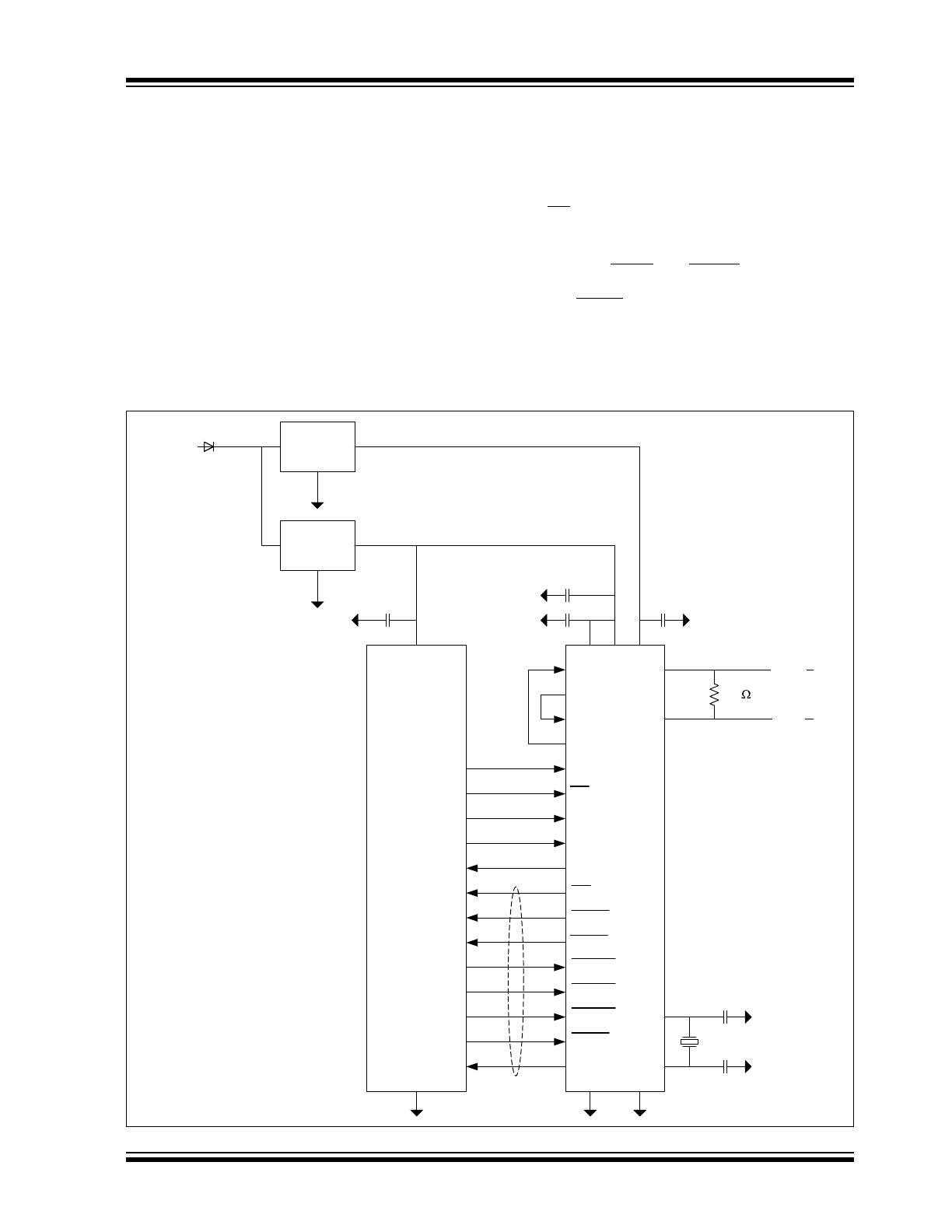
FIGURE 1-2:
MCP25625 INTERFACING WITH A 3.3V MICROCONTROLLER
3.3V LDO
V
DD
V
DDA
T
XD
R
XD
STBY
RA0
V
SS
V
SS
PIC
®
Microcontroller
MCP25625
5V LDO
V
BAT
V
DD
0.1 μF
0.1 μF
CANH
CANL
120
R
xCAN
T
xCAN
V
IO
0.1 μF
GND
OSC2
OSC1
CLKOUT
CS
SCK
INT
SI
SO
R
x1BF
R
x0BF
Tx0RTS
T
x0RTS
T
x0RTS
RESET
OSC1
RA1
SCK
SDI
SDO
INT0
INT1
INT2
RA2
RA3
RA4
RA5
CANH
CANL
0.1 μF
22 pF
22 pF
Optional

MCP25625
DS20005282B-page 6
2014-2017 Microchip Technology Inc.
NOTES:

2014-2017 Microchip Technology Inc.
DS20005282B-page 7
MCP25625
2.0
MODES OF OPERATION
2.1
CAN Controller Modes of
Operation
The CAN controller has five modes of operation:
• Configuration mode
• Normal mode
• Sleep mode
• Listen-Only mode
• Loopback mode
The operational mode is selected via the
REQOP<2:0> bits in the CANCTRL register (see
Register 4-34
).
When changing modes, the mode will not actually
change until all pending message transmissions are
complete. The requested mode must be verified by
reading the OPMOD<2:0> bits in the CANSTAT
register (see
Register 4-35
).
2.2
CAN Transceiver Modes of
Operation
The CAN transceiver has two modes of operation:
• Normal mode
• Standby mode
Normal mode is selected by applying a low level to the
STBY pin. The driver block is operational and can drive
the bus pins. The slopes of the output signals on CANH
and CANL are optimized to produce minimal Electro-
magnetic Emissions (EME). The high-speed differential
receiver is active.
Standby mode is selected by applying a high level to
the STBY pin. In Standby mode, the transmitter and the
high-speed part of the receiver are switched off to min-
imize power consumption. The low-power receiver and
the wake-up filter are enabled in order to monitor the
bus for activity. The receive pin (R
XD
) will show a
delayed representation of the CAN bus, due to the
wake-up filter.
2.3
Configuration Mode
The MCP25625 must be initialized before activation. This
is only possible if the device is in Configuration mode.
Configuration mode is automatically selected after power-
up, a Reset or can be entered from any other mode by
setting the REQOPx bits in the CANCTRL register. When
Configuration mode is entered, all error counters are
cleared. Configuration mode is the only mode where the
following registers are modifiable:
• CNF1, CNF2, CNF3
• TXRTSCTRL
• Acceptance Filter registers
2.4
Normal Mode
Normal mode is the standard operating mode of the
MCP25625. In this mode, the device actively monitors
all bus messages and generates Acknowledge bits,
error frames, etc. This is also the only mode in which
the MCP25625 transmits messages over the CAN bus.
Both the CAN controller and the CAN transceiver must
be in Normal mode.
2.5
Sleep/Standby Mode
The CAN controller has an internal Sleep mode that is
used to minimize the current consumption of the
device. The SPI interface remains active for reading
even when the MCP25625 is in Sleep mode, allowing
access to all registers.
Sleep mode is selected via the REQOPx bits in the
CANCTRL register. The OPMODx bits in the CANSTAT
register indicate the operation mode. These bits should
be read after sending the SLEEP command to the
MCP25625. The MCP25625 is active and has not yet
entered Sleep mode until these bits indicate that Sleep
mode has been entered.
When in Sleep mode, the MCP25625 stops its internal
oscillator. The MCP25625 will wake-up when bus
activity occurs or when the microcontroller sets via the
SPI interface. The WAKIF bit in the CANINTF register
will “generate” a wake-up attempt (the WAKIE bit in the
CANINTE register must also be set in order for the
wake-up interrupt to occur).
The CAN transceiver must be in Standby mode in order
to take advantage of the low standby current of the
transceiver. After a wake-up, the microcontroller must
put the transceiver back into Normal mode using the
STBY pin.

MCP25625
DS20005282B-page 8
2014-2017 Microchip Technology Inc.
2.5.1
WAKE-UP FUNCTIONS
The CAN transceiver will monitor the CAN bus for activity.
The wake-up filter inside the transceiver is enabled to
avoid a wake-up due to noise. In case there is activity on
the CAN bus, the R
XD
pin will go low. The CAN bus wake-
up function requires both CAN transceiver supply volt-
ages to be in a valid range: V
DDA
and V
IO
.
The CAN controller will detect a falling edge on the
RxCAN pin and interrupt the microcontroller if the
wake-up interrupt is enabled.
Since the internal oscillator is shut down while in Sleep
mode, it will take some amount of time for the oscillator
to start-up and the device to enable itself to receive
messages. This Oscillator Start-up Timer (OST) is
defined as 128 T
OSC
.
The device will ignore the message that caused the
wake-up from Sleep mode, as well as any messages
that occur while the device is “waking up”. The device
will wake-up in Listen-Only mode.
The microcontroller must set both the CAN controller
and CAN transceiver to Normal mode before the
MCP25625 will be able to communicate on the bus.
2.6
Listen-Only Mode
Listen-Only mode provides a means for the MCP25625
to receive all messages (including messages with
errors) by configuring the RXM<1:0> bits in the
RXBxCTRL register. This mode can be used for bus
monitor applications or for detecting the baud rate in
“hot plugging” situations.
For Auto-Baud Detection (ABD), it is necessary that at
least two other nodes are communicating with each
other. The baud rate can be detected empirically by
testing different values until valid messages are
received.
Listen-Only mode is a silent mode, meaning no
messages will be transmitted while in this mode
(including error flags or Acknowledge signals). In
Listen-Only mode, both valid and invalid messages will
be received regardless of filters and masks or
RXM<1:0> bits in the RXBxCTRL registers. The error
counters are reset and deactivated in this state. The
Listen-Only mode is activated by setting the REQOPx
bits in the CANCTRL register.
2.7
Loopback Mode
Loopback mode will allow internal transmission of
messages from the transmit buffers to the receive
buffers without actually transmitting messages on the
CAN bus. This mode can be used in system
development and testing.
In this mode, the ACK bit is ignored and the device will
allow incoming messages from itself, just as if they
were coming from another node. The Loopback mode
is a silent mode, meaning no messages will be trans-
mitted while in this state (including error flags or
Acknowledge signals). The TxCAN pin will be in a
Recessive state.
The filters and masks can be used to allow only
particular messages to be loaded into the receive
registers. The masks can be set to all zeros to provide
a mode that accepts all messages. The Loopback
mode is activated by setting the REQOPx bits in the
CANCTRL register.
2014-2017 Microchip Technology Inc.
DS20005282B-page 9
MCP25625
3.0
CAN CONTROLLER
The CAN controller implements the CAN protocol
Version 2.0B. It is compatible with the ISO 11898-1
standard.
Figure 3-1
illustrates the block diagram of the CAN
controller. The CAN controller consists of the following
major blocks:
• CAN protocol engine
• TX handler
• RX handler
• SPI interface
• Control logic with registers and interrupt logic
• I/O pins
• Crystal oscillator
3.1
CAN Module
The CAN protocol engine, together with the TX and RX
handlers, provide all the functions required to receive and
transmit messages on the CAN bus. Messages are trans-
mitted by first loading the appropriate message buffers
and control registers. Transmission is initiated by using
control register bits via the SPI interface or by using the
transmit enable pins. Status and errors can be checked by
reading the appropriate registers. Any message detected
on the CAN bus is checked for errors and then matched
against the user-defined filters to see if it should be moved
into one of the two receive buffers.
3.2
Control Logic
The control logic block controls the setup and operation
of the MCP25625 and contains the registers.
Interrupt pins are provided to allow greater system
flexibility. There is one multipurpose interrupt pin (as
well as specific interrupt pins) for each of the receive
registers that can be used to indicate a valid message
has been received and loaded into one of the receive
buffers. Use of the specific interrupt pins is optional.
The general purpose interrupt pin, as well as Status
registers (accessed via the SPI interface), can also be
used to determine when a valid message has been
received.
Additionally, there are three pins available to initiate
immediate transmission of a message that has been
loaded into one of the three transmit registers. Use of
these pins is optional, as initiating message transmis-
sions can also be accomplished by utilizing control
registers accessed via the SPI interface.
3.3
SPI Protocol Block
The microcontroller interfaces to the device via the SPI
interface. Registers can be accessed using the SPI
READ
and WRITE commands. Specialized SPI
commands reduce the SPI overhead.
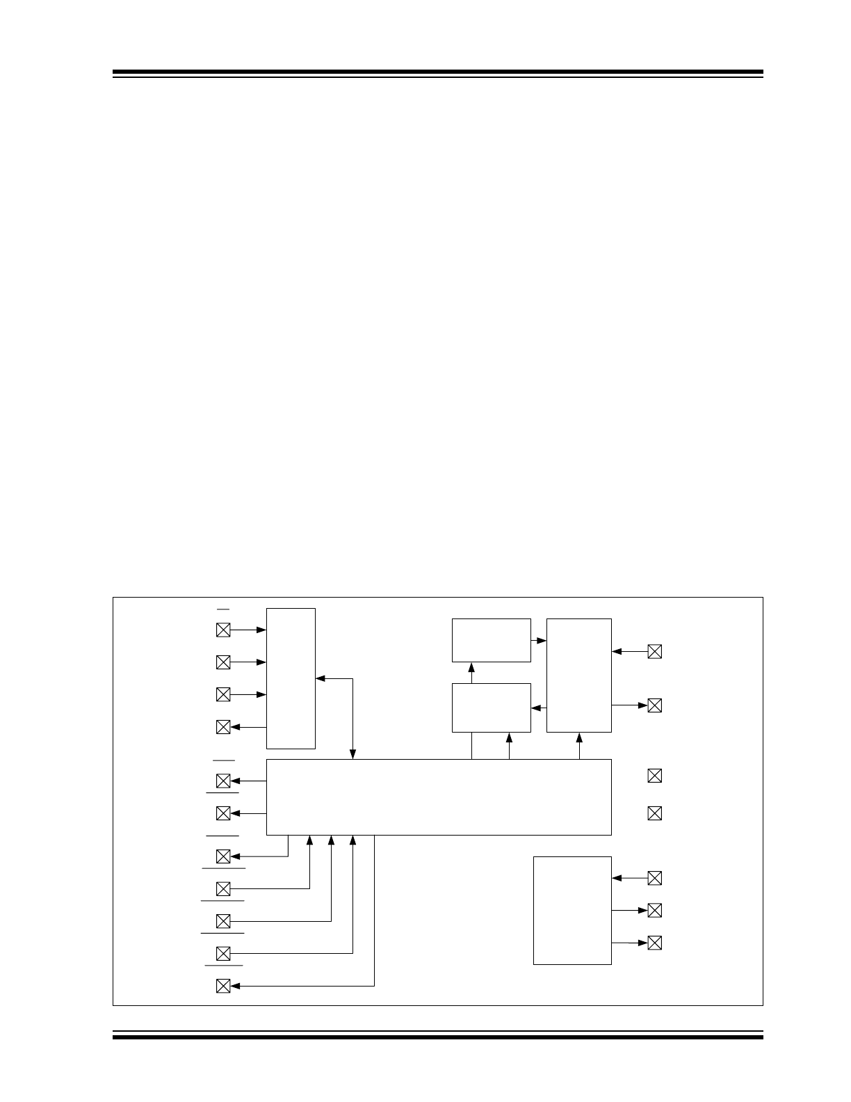
FIGURE 3-1:
CAN CONTROLLER BLOCK DIAGRAM
SPI IF
CAN
Protocol
Engine
Tx Handler
Tx
Prioritization
Control Logic
Registers: Configuration, Control and Interrupts
Rx Handler
Acceptance
Filters and
Masks
TxCAN
RxCAN
CS
SCK
SI
SO
OSC1
OSC2
CLKOUT
INT
Rx0BF
RESET
Crystal
Oscillator
Rx1BF
Tx0RTS
Tx1RTS
Tx2RTS
V
DD
GND
MCP25625
DS20005282B-page 10
2014-2017 Microchip Technology Inc.
3.4
CAN Buffers and Filters
Figure 3-2
shows the CAN buffers and filters in more
detail. The MCP25625 has three transmit and two
receive buffers, two acceptance masks (one per
receive buffer) and a total of six acceptance filters.
FIGURE 3-2:
CAN BUFFERS AND PROTOCOL ENGINE
Acceptance Filter
RXF2
R
X
B
1
Identifier
Data Field
Data Field
Identifier
Acceptance Mask
RXM1
Acceptance Filter
RXF3
Acceptance Filter
RXF4
Acceptance Filter
RXF5
M
A
B
Acceptance Filter
RXF0
Acceptance Filter
RXF1
R
X
B
0
TX
R
E
Q
TXB2
AB
T
F
ML
O
A
TX
E
R
R
MESS
AGE
Message
Queue
Control
Transmit Byte Sequencer
TX
R
E
Q
TXB0
AB
T
F
ML
O
A
TX
E
R
R
MESS
AGE
CRC<14:0>
Comparator
Receive<7:0>
Transmit<7:0>
Receive
Error
Transmit
Error
Protocol
REC
TEC
ErrPas
BusOff
Finite
State
Machine
Counter
Counter
Shift<14:0>
{Transmit<5:0>, Receive<8:0>}
Transmit
Logic
Bit
Timing
Logic
TX
RX
Configuration
Registers
Clock
Generator
PROTOCOL
ENGINE
BUFFERS
TX
R
E
Q
TXB1
AB
T
F
ML
O
A
TX
E
R
R
MESS
AGE
Acceptance Mask
RXM0
A
c
c
e
p
t
A
c
c
e
p
t
SOF