

2015 Microchip Technology Inc.
DS20005409A-page 1
MCP25612FD
Features
• Supports both “classic” CAN 2.0 and CAN FD
physical layer requirements
• Optimized for CAN FD (Flexible Data-Rate) at
2, 5 and 8 Mbps Operation:
- Maximum Propagation Delay: 120 ns
- Loop Delay Symmetry: -10%/+10% (2 Mbps)
• Implements ISO-11898-2 and ISO-11898-5
Standard Physical Layer Requirements
• Very Low Standby Current (5 µA per transceiver,
typical)
• Two Fully Independent V
DDX
and V
SSX
Pins per CAN
FD Transceiver for Added Flexibility and Reliability:
- Optimal for redundant CAN networks
• Compatible to 5V MCUs
• Functional Behavior Predictable Under All Supply
Conditions:
- Device is in Unpowered mode if V
DDX
drops
below undervoltage level
- An unpowered node or brown-out event will
not load the CAN bus
• Detection of Ground Fault:
- Permanent dominant detection on T
XDX
- Permanent dominant detection on bus
• Power-on Reset and Undervoltage Lock-out on
V
DDX
Pin
• Protection against Damage due to Short-Circuit
Conditions (positive or negative battery voltage)
• Protection against High-Voltage Transients in
Automotive Environments
• Automatic Thermal Shutdown Protection
• Suitable for 12V and 24V Systems
• Meets or exceeds Stringent Automotive Design
Requirements, including “Hardware Requirements
for LIN, CAN and FlexRay™ Interfaces in
Automotive Applications”
, Version 1.3, May 2012:
- Conducted emissions @ 2 Mbps with
Common-Mode Choke (CMC)
- Direct Power Injection (DPI) @ 2 Mbps with CMC
• Meets SAE J2962/2 “Communication
Transceivers Qualification Requirements – CAN”
:
- Passes radiated emissions at 2 Mbps without
a CMC
• High Noise Immunity due to Differential Bus
Implementation
• High ESD Protection on CANHx and CANLx,
Meets IEC61000-4-2, up to ±6 kV
• Available in 14-Lead SOIC
• Temperature Ranges:
- Extended (E): -40°C to +125°C
- High (H): -40°C to +150°C
Description
The MCP25612FD is a second generation, dual CAN
FD transceiver from Microchip Technology Inc. It offers
all of the features from two fully independent
MCP2561FD CAN transceivers, except for the SPLIT
pin. It ensures Loop Delay Symmetry in order to support
the higher data rates required for CAN FD. The maxi-
mum propagation delay is improved to support a longer
bus length.
The device meets the automotive requirements for CAN
FD bit rates, low quiescent current, robust
Electromagnetic Compatibility (EMC) and Electrostatic
Discharge (ESD).
Package Types
Typical Applications
Automotive
• Powertrain
• Body Control
• Gateway
• Chassis and Safety
• Infotainment
Industrial
• Factory Automation
• Gateway
• Server Backplanes
• Elevators
• Robotics
CANL1
CANH1
STBY1
T
XD1
MCP25612FD
SOIC
1
2
3
4
5
6
7
14
13
12
11
10
9
8
STBY2
R
XD1
T
XD2
V
SS2
V
DD2
R
XD2
CANL2
CANH2
V
DD1
V
SS1
Dual CAN Flexible Data-Rate Transceiver
MCP25612FD
DS20005409A-page 2
2015 Microchip Technology Inc.
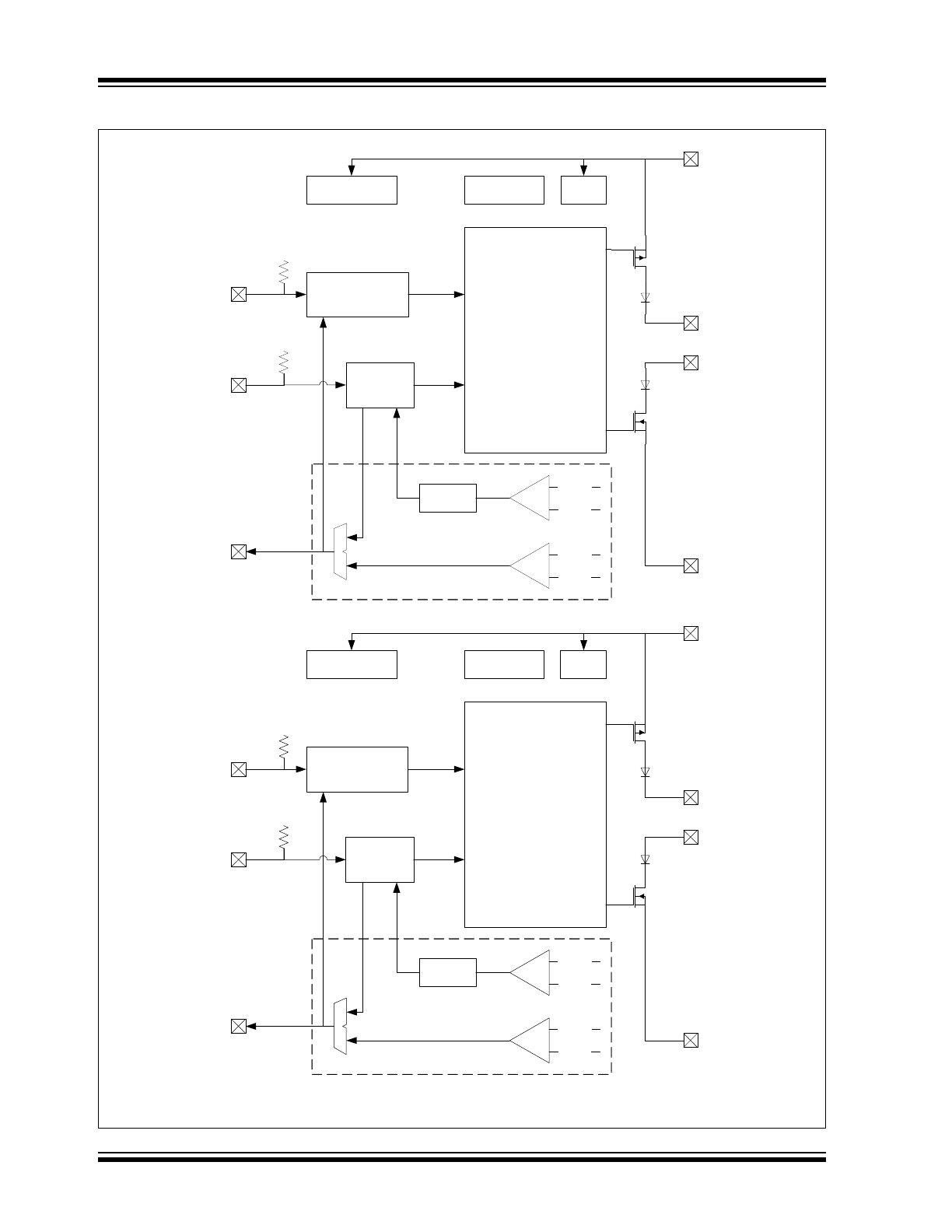
Device Block Diagram
Note 1:
There is only one receiver implemented. The receiver can operate in either Low-Power or High-Speed mode.
V
DD1
CANH1
CANL1
T
XD1
R
XD1
Driver
and
Slope Control
Thermal
Protection
POR
UVLO
Digital I/O
Supply
V
SS1
STBY1
Permanent
Dominant Detect
V
DD1
V
DD1
Mode
Control
Wake-up
Filter
CANH1
CANL1
CANH1
CANL1
Receiver
LP_RX
HS_RX
V
DD2
CANH2
CANL2
T
XD2
R
XD2
Driver
and
Slope Control
Thermal
Protection
POR
UVLO
Digital I/O
Supply
V
SS2
STBY2
Permanent
Dominant Detect
V
DD2
V
DD2
Mode
Control
Wake-up
Filter
CANH1
CANL1
CANH1
CANL1
Receiver
LP_RX
HS_RX
(
Note 1
)
2015 Microchip Technology Inc.
DS20005409A-page 3
MCP25612FD
1.0
DEVICE OVERVIEW
The MCP25612FD is a dual fully independent, CAN
FD transceiver Fault tolerant device that serves as the
interface between a CAN protocol controller and the
physical bus. The MCP25612FD device provides differ-
ential transmit and receive capability for the CAN pro-
tocol controller, and is fully compatible with the ISO
11898-2 and ISO 11898-5 standards.
The Loop Delay Symmetry is ensured to support data
rates up to 8 Mbps for CAN FD (Flexible Data-Rate).
The maximum propagation delay was improved to
support longer bus length.
Typically, each node in a CAN system must have a
device to convert the digital signals generated by a
CAN controller to signals suitable for transmission over
the bus cabling (differential output). It also provides a
buffer between the CAN controller and the high-voltage
spikes that can be generated on the CAN bus by
outside sources.
1.1
Mode Control Block
The MCP25612FD supports two modes of operation
between the two CAN transceivers independently:
• Normal Mode
• Standby Mode
These modes are summarized in
Table 1-1
.
1.1.1
NORMAL MODE
Normal mode is selected by applying low-level voltage
to the STBYx pin. The driver block is operational and
can drive the bus pins. The slopes of the output signals
on CANHx and CANLx are optimized to produce
minimal Electromagnetic Emissions (EME).
The high-speed differential receiver is active.
1.1.2
STANDBY MODE
The device may be placed in Standby mode by apply-
ing a high-level voltage to the STBYx pin. In Standby
mode, the transmitter and the high-speed part of the
receiver are switched off to minimize power consump-
tion. The low-power receiver and the wake-up filter
blocks are enabled to monitor the bus for activity. The
Receive pin (R
XDX
) will show a delayed representation
of the CAN bus due to the wake-up filter.
The CAN controller gets interrupted by a negative edge
on the R
XDX
pin (Dominant state on the CAN bus). The
CAN controller must put the MCP25612FD back into
Normal mode, using the STBYx pin, in order to enable
high-speed data communication.
The CAN bus wake-up function requires V
DDX
to be in
valid range.
TABLE 1-1:
MODES OF OPERATION
Mode
STBYx Pin
R
XDX
Pin
Low
High
Normal
Low
Bus is dominant
Bus is recessive
Standby
High
Wake-up request is detected
No wake-up request detected

MCP25612FD
DS20005409A-page 4
2015 Microchip Technology Inc.
1.2
Transmitter Function
The CAN bus has two states:
• Dominant state
• Recessive state
A Dominant state occurs when the differential voltage
between CANHx and CANLx is greater than
V
DIFFX(D)(I)
. A Recessive state occurs when the differ-
ential voltage is less than V
DIFFX(R)(I)
. The Dominant
and Recessive states correspond to the Low and High
state of the T
XDX
input pin, respectively. However, a
Dominant state initiated by another CAN node will
override a Recessive state on the CAN bus.
1.3
Receiver Function
In Normal mode, the R
XDX
output pin reflects the
differential bus voltage between CANHx and CANLx.
The Low and High states of the R
XDX
output pin
correspond to the Dominant and Recessive states of
the CAN bus, respectively.
1.4
Internal Protection
CANHx and CANLx are protected against battery short
circuits and electrical transients that can occur on the
CAN bus. This feature prevents destruction of the
transmitter output stage during such a Fault condition.
The device is further protected from excessive current
loading by thermal shutdown circuitry that disables the
output drivers when the junction temperature exceeds
a nominal limit of +175°C. All other parts of the chip
remain operational and the chip temperature is lowered
due to the decreased power dissipation in the transmitter
outputs. This protection is essential to protect against
bus line short-circuit induced damage. The activation of
the internal protection in one of the transceivers will not
affect the other one since these are fully independent.
1.5
Permanent Dominant Detection
The MCP25612FD device prevents two conditions:
• Permanent dominant condition on T
XDX
• Permanent dominant condition on the bus
In Normal mode, if the MCP25612FD detects an
extended Low state on the T
XDX
input, it will disable the
CANHx and CANLx output drivers in order to prevent
the corruption of data on the CAN bus. The drivers will
remain disabled until T
XDX
goes to the High state.
In Standby mode, if the MCP25612FD detects an
extended Dominant condition on the bus, it will set the
R
XDX
pin to the Recessive state. This allows the
attached controller to go to Low-Power mode until the
dominant issue is corrected. R
XDX
is latched high until
a Recessive state is detected on the bus and the
wake-up function is enabled again.
Both conditions have a time-out of 1.25 ms (typical).
This implies a maximum bit time of 69.44 µs (14.4 kHz),
allowing up to 18 consecutive dominant bits on the bus.
The permanent dominant detection in one of the
transceivers will not affect the other one since these
are fully independent.
1.6
Power-on Reset (POR) and
Undervoltage Detection
The MCP25612FD has undervoltage detection on
the V
DDX
supply pin. The typical undervoltage
threshold is 4V.
When the device is powered on, CANHx and CANLx
remain in a High-Impedance state until V
DDX
exceeds
its undervoltage level. Once powered on, CANHx and
CANLx will enter a High-Impedance state if the voltage
level at V
DDX
drops below the undervoltage level,
providing voltage brown-out protection during normal
operation.
In Normal mode, the receiver output is forced to the
Recessive state during an undervoltage condition on
V
DDX
. In Standby mode, the low-power receiver is only
enabled when the V
DDX
supply voltage rises above its
undervoltage threshold. Once the threshold voltage is
reached, the low-power receiver is no longer controlled
by the POR comparator and remains operational down
to about 2.5V on the V
DDX
supply.

2015 Microchip Technology Inc.
DS20005409A-page 5
MCP25612FD
2.0
ELECTRICAL
CHARACTERISTICS
2.1
Absolute Maximum Ratings
†
V
DDX
...........................................................................................................................................................................7.0V
DC Voltage at T
XDX
, R
XDX
, STBYx and V
SSX
..................................................................................-0.3V to V
DDX
+ 0.3V
DC Voltage at CANHx and CANLx............................................................................................................... -58V to +58V
Transient Voltage on CANHx, CANLx (ISO-7637) (see
Figure 2-4
)......................................................... -150V to +100V
Storage Temperature ..............................................................................................................................-55°C to +150°C
Operating Ambient Temperature.............................................................................................................-40°C to +150°C
Virtual Junction Temperature, T
VJ
(IEC60747-1) ....................................................................................-40°C to +190°C
Soldering Temperature of Leads (10 seconds) ..................................................................................................... +300°C
ESD Protection on CANHx and CANLx Pins (IEC 61000-4-2); 330Ω/150 pF; Unpowered; Contact Discharge...... ±6 kV
ESD Protection on CANHx and CANLx Pins (IEC 801; Human Body Model); 1500Ω/100 pF ................................ ±8 kV
ESD Protection on All Other Pins (IEC 801; Human Body Model); 1500Ω/100 pF.................................................. ±4 kV
ESD Protection on All Pins (IEC 801; Machine Model); 0Ω/200 pF........................................................................±300V
ESD Protection on All Pins (IEC 801; Charge Device Model).................................................................................±750V
2.2
Specifications
† NOTICE:
Stresses above those listed under “Maximum ratings” may cause permanent damage to the device. This
is a stress rating only and functional operation of the device at those or any other conditions above those indicated
in the operational listings of this specification is not implied. Exposure to maximum rating conditions for extended
periods may affect device reliability.
TABLE 2-1:
DC ELECTRICAL SPECIFICATIONS
Electrical Characteristics:
Extended (E): T
AMB
= -40°C to +125°C; High (H): T
AMB
= -40°C to +150°C;
V
DDX
= 4.5V to 5.5V, R
LX
= 60Ω, C
LX
= 100 pF; unless otherwise specified.
Characteristic
Sym
Min
Typ
Max
Units
Conditions
Supply (V
DDX
Pin)
Voltage Range
V
DDX
4.5
—
5.5
Supply Current
(per transceiver)
I
DD
—
5
10
mA Recessive; V
TXDX
= V
DDX
—
45
70
Dominant; V
TXDX
= 0V
Standby Current
(per transceiver)
I
DDS
—
5
15
µA
High Level of the POR
Comparator
V
PORH
3.8
—
4.3
V
Low Level of the POR
Comparator
V
PORL
3.4
—
4.0
V
Hysteresis of the POR
Comparator
V
PORD
0.3
—
0.8
V
Note 1:
Characterized; not 100% tested.
2:
-12V to 12V is ensured by characterization, tested from -2V to 7V.

MCP25612FD
DS20005409A-page 6
2015 Microchip Technology Inc.
Bus Line Transmitter (CANHx, CANLx)
CANHx, CANLx:
Recessive Bus Output Voltage
V
O(R)
2.0
0.5 V
DDX
3.0
V
V
TXDX
= V
DDX
; no load
CANHx, CANLx:
Bus Output Voltage in Standby
V
O(S)
-0.1
0.0
+0.1
V
STBYx = V
TXDX
= V
DDX
; no load
Recessive Output Current
I
O(R)
-5
—
+5
mA -24V < V
CAN
< +24V
CANHx: Dominant
Output Voltage
V
O(D)
2.75
3.50
4.50
V
T
TXDX
= 0; R
LX
= 50 to 65Ω
CANLx: Dominant
Output Voltage
0.50
1.50
2.25
R
LX
= 50 to 65Ω
Symmetry of Dominant
Output Voltage
(V
DDX
– V
CANHX
– V
CANLX
)
V
O(D)(M)
-400
0
+400
mV V
TXDX
= V
SSX
(
Note 1
)
Dominant: Differential
Output Voltage
V
O(DIFF)
1.5
2.0
3.0
V
V
TXDX
= V
SSX
; R
LX
= 50 to 65Ω
(see
Figure 2-1
and
Figure 2-3
)
Recessive:
Differential Output Voltage
-120
0
12
mV V
TXDX
= V
DDX
(see
Figure 2-1
and
Figure 2-3
)
-500
0
50
mV V
TXDX
= V
DDX
; no load
(see
Figure 2-1
and
Figure 2-3
)
CANHx: Short-Circuit
Output Current
I
O(SC)
-120
85
—
mA V
TXDX
= V
SSX
; V
CANHX
= 0V;
CANLx: Floating
-100
—
—
mA Same as above, but V
DDX
= 5V;
T
AMB
= +25°C (
Note 1
)
CANLx: Short-Circuit
Output Current
—
75
+120
mA V
TXDX
= V
SSX
; V
CANLX
= 18V;
CANHx: Floating
—
—
+100
mA Same as above, but V
DDX
= 5V;
T
AMB
= +25°C (
Note 1
)
Bus Line Receiver (CANHx, CANLx)
Recessive Differential
Input Voltage
V
DIFFX(R)(I)
-1.0
—
+0.5
V
Normal mode;
-12V < V
(CANHX
,
CANLX)
< +12V
(see
Figure 2-5
) (
Note 2
)
-1.0
—
+0.4
Standby mode;
-12V < V
(CANHX
,
CANLX)
< +12V
(see
Figure 2-5
) (
Note 2
)
Dominant Differential
Input Voltage
V
DIFFX(D)(I)
0.9
—
V
DDX
V
Normal mode;
-12V < V
(CANHX
,
CANLX)
< +12V
(see
Figure 2-5
) (
Note 2
)
1.0
—
V
DDX
Standby mode;
-12V < V
(CANHX
,
CANLX)
< +12V
(see
Figure 2-5
) (
Note 2
)
TABLE 2-1:
DC ELECTRICAL SPECIFICATIONS (CONTINUED)
Electrical Characteristics:
Extended (E): T
AMB
= -40°C to +125°C; High (H): T
AMB
= -40°C to +150°C;
V
DDX
= 4.5V to 5.5V, R
LX
= 60Ω, C
LX
= 100 pF; unless otherwise specified.
Characteristic
Sym
Min
Typ
Max
Units
Conditions
Note 1:
Characterized; not 100% tested.
2:
-12V to 12V is ensured by characterization, tested from -2V to 7V.

2015 Microchip Technology Inc.
DS20005409A-page 7
MCP25612FD
Bus Line Receiver (CANHx, CANLx) (Continued)
Differential
Receiver Threshold
V
TH(DIFF)
0.5
0.7
0.9
V
Normal mode;
-12V < V
(CANHX, CANLX)
< +12V
(see
Figure 2-5
) (
Note 2
)
0.4
—
1.0
Standby mode;
-12V < V
(CANHX, CANLX)
< +12V
(see
Figure 2-5
) (
Note 2
)
Differential
Input Hysteresis
V
HYS(DIFF)
50
—
200
mV Normal mode (see
Figure 2-5
)
(
Note 1
)
Common-Mode
Input Resistance
R
IN
10
—
30
kΩ
(
Note 1
)
Common-Mode
Resistance Matching
R
IN(M)
-1
0
+1
%
V
CANHX
= V
CANLX
(
Note 1
)
Differential Input Resistance
R
IN(DIFF)
10
—
100
kΩ
(
Note 1
)
Common-Mode
Input Capacitance
C
IN(CM)
—
—
20
pF
V
TXDX
= V
DDX
(
Note 1
)
Differential
Input Capacitance
C
IN(DIFF)
—
—
10
V
TXDX
= V
DDX
(
Note 1
)
CANHx, CANLx:
Input Leakage
I
LI
-5
—
+5
µA
V
DDX
= V
TXDX
= V
STBYX
= 0V;
V
CANHX
= V
CANLX
= 5V
Digital Input Pins (T
XDX
, STBYx)
High-Level Input Voltage
V
IH
0.7 V
DDX
—
V
DDX
+ 0.3
V
Low-Level Input Voltage
V
IL
-0.3
—
0.3 V
DDX
V
High-Level Input Current
I
IH
-1
—
+1
µA
T
XDX
: Low-Level Input Current
I
IL(TXDX)
-270
-150
-30
µA
STBYx: Low-Level Input
Current
I
IL(STBYX)
-30
—
-1
µA
Receive Data Output (R
XDX
)
High-Level Output Voltage
V
OHX
V
DDX
– 0.4
—
—
V
I
OH
= -2 mA; typical -4 mA
Low-Level Output Voltage
V
OLX
—
—
0.4
V
I
OL
= 4 mA; typical 8 mA
Thermal Shutdown
Shutdown
Junction Temperature
T
J(SD)
165
175
185
°C
-12V < V
(CANHX, CANLX)
< +12V
(
Note 1
)
Shutdown
Temperature Hysteresis
T
J(HYST)
20
—
30
°C
-12V < V
(CANHX, CANLX)
< +12V
(
Note 1
)
TABLE 2-1:
DC ELECTRICAL SPECIFICATIONS (CONTINUED)
Electrical Characteristics:
Extended (E): T
AMB
= -40°C to +125°C; High (H): T
AMB
= -40°C to +150°C;
V
DDX
= 4.5V to 5.5V, R
LX
= 60Ω, C
LX
= 100 pF; unless otherwise specified.
Characteristic
Sym
Min
Typ
Max
Units
Conditions
Note 1:
Characterized; not 100% tested.
2:
-12V to 12V is ensured by characterization, tested from -2V to 7V.
MCP25612FD
DS20005409A-page 8
2015 Microchip Technology Inc.
FIGURE 2-1:
Physical Bit Representation and Simplified Bias Implementation.
CA
N
H
X
,
C
AN
L
X
Time
CANH
X
CANL
X
Normal Mode
Standby Mode
Recessive
Recessive
Dominant
CANL
X
CANH
X
V
DDX
/2
R
XDX
V
DDX
Normal
Standby
Mode
2015 Microchip Technology Inc.
DS20005409A-page 9
MCP25612FD
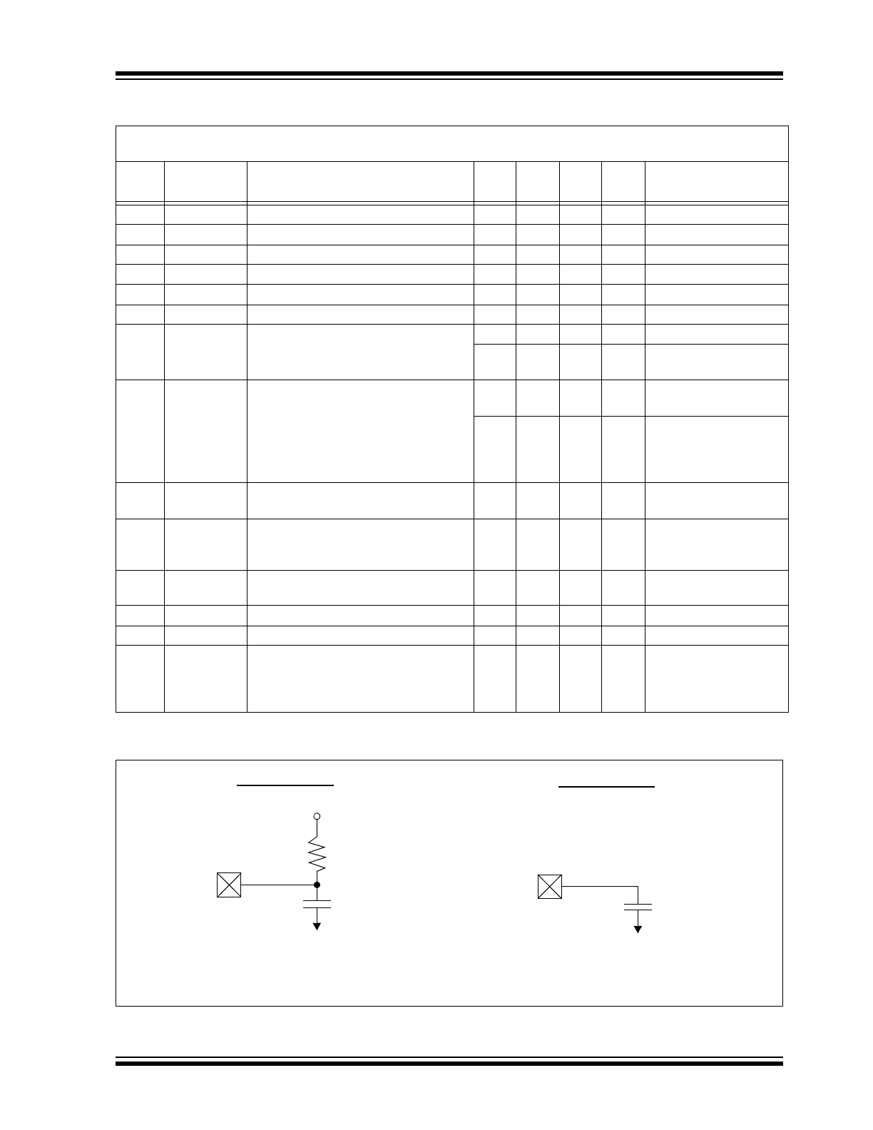
FIGURE 2-2:
Test Load Conditions.
TABLE 2-2:
AC ELECTRICAL SPECIFICATIONS
Electrical Characteristics:
Extended (E): T
AMB
= -40°C to +125°C; High (H): T
AMB
= -40°C to +150°C;
V
DDX
= 4.5V to 5.5V, R
LX
= 60Ω
C
LX
= 100 pF; unless otherwise specified.
Param.
No.
Sym
Characteristic
Min
Typ
Max
Units
Conditions
1
t
BIT
Bit Time
0.125
—
69.44
µs
2
f
BIT
Bit Frequency
14.4
—
8000
kHz
3
t
TXDX-BUSON
Delay T
XDX
Low to Bus Dominant
—
65
—
ns
(
Note 1
)
4
t
TXDX-BUSOFF
Delay T
XDX
High to Bus Recessive
—
90
—
ns
(
Note 1
)
5
t
BUSON-RXDX
Delay Bus Dominant to R
XDX
—
60
—
ns
(
Note 1
)
6
t
BUSOFF-RXDX
Delay Bus Recessive to R
XDX
—
65
—
ns
(
Note 1
)
7
t
TXDX-RXDX
Propagation Delay T
XDX
to R
XDX
—
90
120
ns
—
120
180
ns
R
LX
= 120Ω,
C
LX
= 200 pF (
Note 1
)
8a
t
BIT(RXDX),2M
Recessive Bit Time on R
XDX
– 2 Mbps,
Loop Delay Symmetry
450
485
550
ns
t
BIT(TXDX)
= 500 ns
(see
Figure 2-10
)
400
460
550
ns
t
BIT(TXDX)
= 500 ns
(see
Figure 2-10
);
R
LX
= 120Ω,
C
LX
= 200 pF (
Note 1
)
8b
t
BIT(RXDX),5M
Recessive Bit Time on R
XDX
– 5 Mbps,
Loop Delay Symmetry
160
185
220
ns
t
BIT(TXDX)
= 200 ns
(see
Figure 2-10
)
8c
t
BIT(RXDX),8M
Recessive Bit Time on R
XDX
– 8 Mbps,
Loop Delay Symmetry
85
105
140
ns
t
BIT(TXDX)
= 120 ns
(see
Figure 2-10
)
(
Note 1
)
9
t
FLTR(WAKE)
Delay Bus Dominant to R
XDX
(Standby mode)
0.5
1
4
µs
Standby mode
10
t
WAKE
Delay Standby to Normal Mode
5
25
40
µs
Negative edge on STBYx
11
t
PDT
Permanent Dominant Detect Time
—
1.25
—
ms
T
XDX
= 0V
12
t
PDTR
Permanent Dominant Timer Reset
—
100
—
ns
The shortest Recessive
pulse on T
XDX
or CAN
bus to reset Permanent
Dominant Timer
Note 1:
Characterized, not 100% tested.
V
DDX
/2
C
LX
R
LX
Pin
Pin
V
SSX
V
SSX
C
LX
R
LX
= 464Ω
C
LX
= 50 pF for all digital pins
Load Condition 1
Load Condition 2
MCP25612FD
DS20005409A-page 10
2015 Microchip Technology Inc.
FIGURE 2-3:
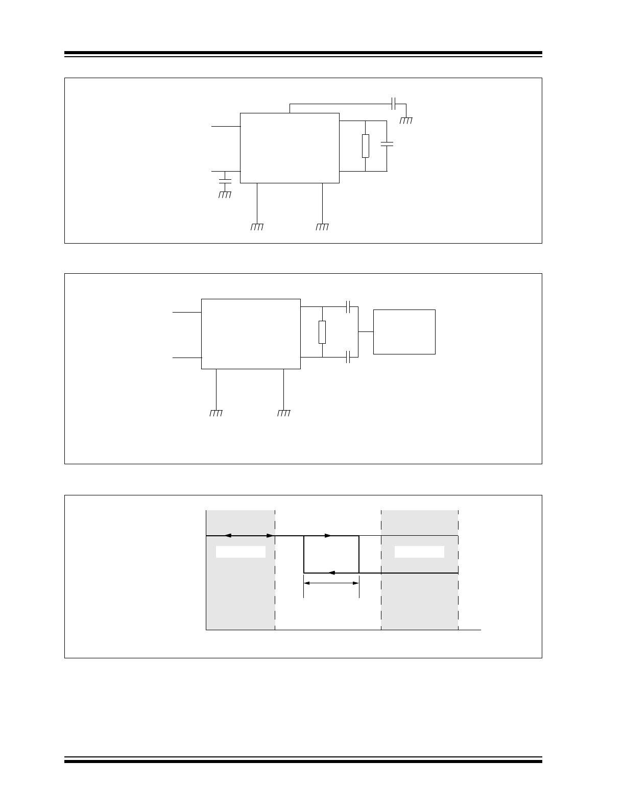
Test Circuit for Electrical Characteristics.
FIGURE 2-4:
Test Circuit for Automotive Transients.
FIGURE 2-5:
Hysteresis of the Receiver.
GNDx
R
XDX
T
XDX
R
LX
C
LX
15 pF
CANHx
CANLx
CAN
Transceiver
0.1 µF
V
DDX
STBYx
GNDx
R
XDX
T
XDX
R
LX
1000 pF
1000 pF
Note 1:
The waveforms of the applied transients shall be in accordance with ISO-7637, Part 1,
Test Pulses 1, 2, 3a and 3b.
CANHx
CANLx
CAN
Transceiver
Transient
Generator
STBYx
(
Note 1
)
V
OHX
V
OLX
0.5
0.9
V
DIFFX
(V)
R
XDX
(Receive Data
Output Voltage)
V
DIFFX(R)(I)
V
DIFFX(H)(I)
V
DIFFX(D)(I)