
2014 Microchip Technology Inc.
DS20005284A-page 1
MCP2561/2FD
Features:
• Optimized for CAN FD (Flexible Data rate) at 2, 5
and 8 Mbps Operation
- Maximum Propagation Delay: 120 ns
- Loop Delay Symmetry: -10%/+10% (2 Mbps)
• Implements ISO-11898-2 and ISO-11898-5
Standard Physical Layer Requirements
• Very Low Standby Current (5 µA, typical)
• V
IO
Supply Pin to Interface Directly to
CAN Controllers and Microcontrollers with
1.8V to 5.5V I/O
• SPLIT Output Pin to Stabilize Common Mode in
Biased Split Termination Schemes
• CAN Bus Pins are Disconnected when Device is
Unpowered
- An Unpowered Node or Brown-Out Event will
Not Load the CAN Bus
• Detection of Ground Fault:
- Permanent Dominant Detection on T
XD
- Permanent Dominant Detection on Bus
• Power-on Reset and Voltage Brown-Out
Protection on V
DD
Pin
• Protection Against Damage Due to Short-Circuit
Conditions (Positive or Negative Battery Voltage)
• Protection Against High-Voltage Transients in
Automotive Environments
• Automatic Thermal Shutdown Protection
• Suitable for 12V and 24V Systems
• Meets or exceeds stringent automotive design
requirements including “Hardware Requirements
for LIN, CAN and FlexRay Interfaces in
Automotive Applications”, Version 1.3, May 2012
- Radiated emissions @ 2 Mbps with Common
Mode Choke (CMC)
- DPI @ 2 Mbps with CMC
• High ESD Protection on CANH and CANL,
meeting IEC61000-4-2 up to ±14 kV
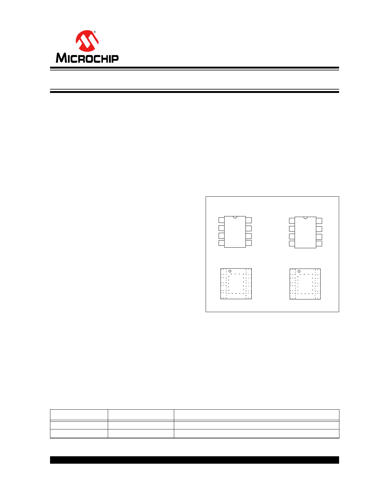
• Available in PDIP-8L, SOIC-8L and 3x3 DFN-8L
• Temperature ranges:
- Extended (E): -40°C to +125°C
- High (H): -40°C to +150°C
Description:
The MCP2561/2FD is a second generation high-speed
CAN transceiver from Microchip Technology Inc. It
offers the same features as the MCP2561/2.
Additionally, it guarantees Loop Delay Symmetry in
order to support the higher data rates required for CAN
FD. The maximum propagation delay was improved to
support longer bus length.
The device meets the automotive requirements for
CAN FD bit rates exceeding 2 Mbps, low quiescent
current, electromagnetic compatibility (EMC) and
electrostatic discharge (ESD).
Package Types
MCP2561/2FD Family Members
MCP2562FD
PDIP, SOIC
V
DD
V
SS
R
XD
CANH
CANL
1
2
3
4
8
7
6
5 V
IO
STBY
T
XD
MCP2561FD
PDIP, SOIC
V
DD
V
SS
R
XD
CANH
CANL
1
2
3
4
8
7
6
5 SPLIT
STBY
T
XD
MCP2561FD
3x3 DFN*
V
DD
V
SS
R
XD
CANH
CANL
1
2
3
4
8
7
6
5 SPLIT
STBY
T
XD
EP
9
MCP2562FD
3x3 DFN*
V
DD
V
SS
R
XD
CANH
CANL
1
2
3
4
8
7
6
5 V
IO
STBY
T
XD
EP
9
* Includes Exposed Thermal Pad (EP); see Table 1-2
Device
Feature
Description
MCP2561FD
SPLIT pin
Common mode stabilization
MCP2562FD
V
IO
pin
Internal level shifter on digital I/O pins
Note: For ordering information, see the “Product Identification System” section on page 29.
High-Speed CAN Flexible Data Rate Transceiver
MCP2561/2FD
DS20005284A-page 2
2014 Microchip Technology Inc.
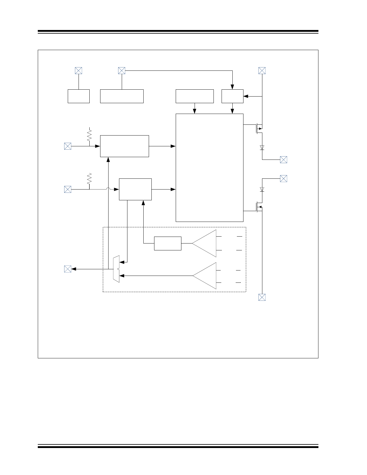
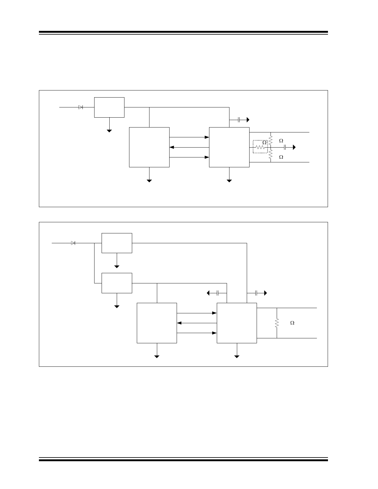
Block Diagram
Note 1: There is only one receiver implemented. The receiver can operate in Low-Power or High-Speed mode.
2: Only MCP2561FD has the SPLIT pin.
3: Only MCP2562FD has the V
IO
pin. In MCP2561FD, the supply for the digital I/O is internally connected
to V
DD
.
V
DD
CANH
CANL
T
XD
R
XD
Driver
and
Slope Control
Thermal
Protection
POR
UVLO
Digital I/O
Supply
V
IO
(3)
V
SS
STBY
Permanent
Dominant Detect
V
IO
V
IO
Mode
Control
V
DD
/2
SPLIT
(2 )
Wake-Up
Filter
CANH
CANL
CANH
CANL
Receiver
LP_RX
(1)
HS_RX
2014 Microchip Technology Inc.
DS20005284A-page 3
MCP2561/2FD
1.0
DEVICE OVERVIEW
The MCP2561/2FD is a high-speed CAN device,
fault-tolerant device that serves as the interface
between a CAN protocol controller and the physical
bus. The MCP2561/2FD device provides differential
transmit and receive capability for the CAN protocol
controller, and is fully compatible with the ISO-11898-2
and ISO-11898-5 standards.
The Loop Delay Symmetry is guaranteed to support
data rates that are up to 5 Mbps for CAN FD (Flexible
Data rate). The maximum propagation delay was
improved to support longer bus length.
Typically, each node in a CAN system must have a
device to convert the digital signals generated by a
CAN controller to signals suitable for transmission over
the bus cabling (differential output). It also provides a
buffer between the CAN controller and the high-voltage
spikes that can be generated on the CAN bus by
outside sources.
1.1
Mode Control Block
The MCP2561/2FD supports two modes of operation:
• Normal Mode
• Standby Mode
These modes are summarized in Table 1-1.
1.1.1
NORMAL MODE
Normal mode is selected by applying low-level voltage
to the STBY pin. The driver block is operational and
can drive the bus pins. The slopes of the output signals
on CANH and CANL are optimized to produce minimal
electromagnetic emissions (EME).
The high speed differential receiver is active.
1.1.2
STANDBY MODE
The device may be placed in Standby mode by
applying high-level voltage to the STBY pin. In Standby
mode, the transmitter and the high-speed part of the
receiver are switched off to minimize power
consumption. The low-power receiver and the wake-up
filter blocks are enabled to monitor the bus for activity.
The receive pin (R
XD
) will show a delayed
representation of the CAN bus, due to the wake-up
filter.
The CAN controller gets interrupted by a negative edge
on the R
XD
pin (Dominant state on the CAN bus). The
CAN controller must put the MCP2561/2FD back into
Normal mode, using the STBY pin, in order to enable
high speed data communication.
The CAN bus wake-up function requires both supply
voltages, V
DD
and V
IO
, to be in valid range.
1.2
Transmitter Function
The CAN bus has two states:
• Dominant State
• Recessive State
A Dominant state occurs when the differential voltage
between CANH and CANL is greater than V
DIFF
(
D
)(
I
).
A Recessive state occurs when the differential voltage
is less than V
DIFF
(
R
)(
I
). The Dominant and Recessive
states correspond to the Low and High state of the T
XD
input pin, respectively. However, a Dominant state
initiated by another CAN node will override a
Recessive state on the CAN bus.
1.3
Receiver Function
In Normal mode, the R
XD
output pin reflects the
differential bus voltage between CANH and CANL. The
Low and High states of the R
XD
output pin correspond
to the Dominant and Recessive states of the CAN bus,
respectively.
1.4
Internal Protection
CANH and CANL are protected against battery
short-circuits and electrical transients that can occur on
the CAN bus. This feature prevents destruction of the
transmitter output stage during such a fault condition.
The device is further protected from excessive current
loading by thermal shutdown circuitry that disables the
output drivers when the junction temperature exceeds
a nominal limit of +175°C. All other parts of the chip
remain operational, and the chip temperature is
lowered due to the decreased power dissipation in the
transmitter outputs. This protection is essential to
protect against bus line short-circuit-induced damage.
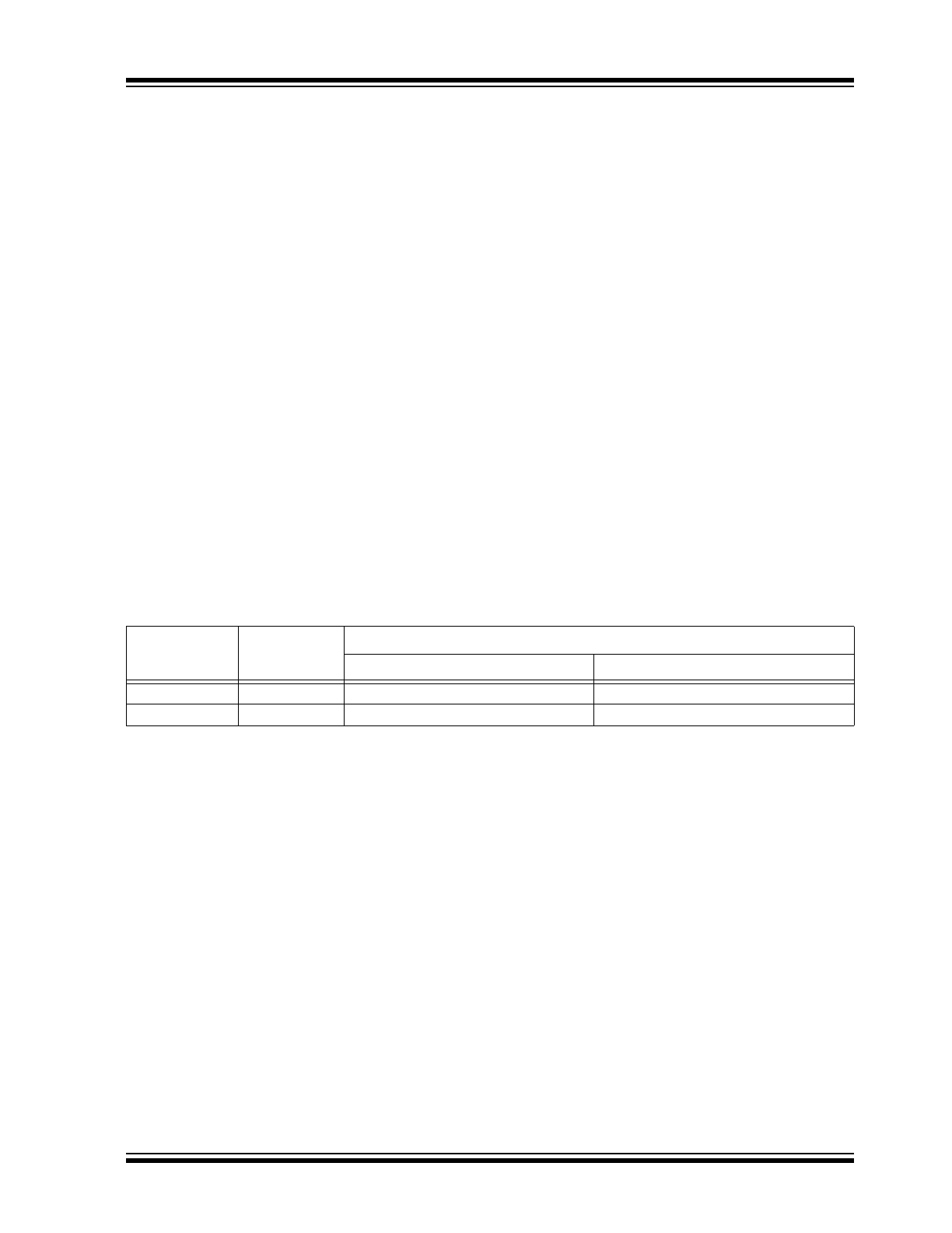
TABLE 1-1:
MODES OF OPERATION
Mode
STBY Pin
R
XD
Pin
LOW
HIGH
Normal
LOW
Bus is Dominant
Bus is Recessive
Standby
HIGH
Wake-up request is detected
No wake-up request detected
MCP2561/2FD
DS20005284A-page 4
2014 Microchip Technology Inc.
1.5
Permanent Dominant Detection
The MCP2561/2FD device prevents two conditions:
• Permanent Dominant condition on T
XD
• Permanent Dominant condition on the bus
In Normal mode, if the MCP2561/2FD detects an
extended Low state on the T
XD
input, it will disable the
CANH and CANL output drivers in order to prevent the
corruption of data on the CAN bus. The drivers will
remain disabled until T
XD
goes High.
In Standby mode, if the MCP2561/2FD detects an
extended Dominant condition on the bus, it will set the
R
XD
pin to Recessive state. This allows the attached
controller to go to Low-Power mode until the Dominant
issue is corrected. R
XD
is latched High until a
Recessive state is detected on the bus, and the
wake-up function is enabled again.
Both conditions have a time-out of 1.25 ms (typical).
This implies a maximum bit time of 69.44 µs
(14.4 kHz), allowing up to 18 consecutive dominant bits
on the bus.
1.6
Power-On Reset (POR) and
Undervoltage Detection
The MCP2561/2FD has undervoltage detection on
both supply pins: V
DD
and V
IO
. Typical undervoltage
thresholds are 1.2V for V
IO
and 4V for V
DD
.
When the device is powered on, CANH and CANL
remain in a high-impedance state until both V
DD
and
V
IO
exceed their undervoltage levels. Once powered
on, CANH and CANL will enter a high-impedance state
if the voltage level at V
DD
drops below the undervoltage
level, providing voltage brown-out protection during
normal operation.
In Normal mode, the receiver output is forced to
Recessive state during an undervoltage condition on
V
DD
. In Standby mode, the low-power receiver is only
enabled when both V
DD
and V
IO
supply voltages rise
above their respective undervoltage thresholds. Once
these threshold voltages are reached, the low-power
receiver is no longer controlled by the POR comparator
and remains operational down to about 2.5V on the
V
DD
supply (MCP2561/2FD). The MCP2562FD
transfers data to the R
XD
pin down to 1.8V on the V
IO
supply.
1.7
Pin Descriptions
Table 1-2 describes the pinout.
TABLE 1-2:
MCP2561/2FD PIN DESCRIPTIONS
MCP2561FD
3x3 DFN
MCP2561FD
PDIP, SOIC
MCP2562FD
3x3 DFN
MCP2562FD
PDIP, SOIC
Symbol
Pin Function
1
1
1
1
T
XD
Transmit Data Input
2
2
2
2
V
SS
Ground
3
3
3
3
V
DD
Supply Voltage
4
4
4
4
R
XD
Receive Data Output
5
5
—
—
SPLIT
Common Mode Stabilization - MCP2561FD only
—
—
5
5
V
IO
Digital I/O Supply Pin - MCP2562FD only
6
6
6
6
CANL
CAN Low-Level Voltage I/O
7
7
7
7
CANH CAN High-Level Voltage I/O
8
8
8
8
STBY
Standby Mode Input
9
—
9
—
EP
Exposed Thermal Pad

2014 Microchip Technology Inc.
DS20005284A-page 5
MCP2561/2FD
1.7.1
TRANSMITTER DATA
INPUT PIN (T
XD
)
The CAN transceiver drives the differential output pins
CANH and CANL according to T
XD
. It is usually
connected to the transmitter data output of the CAN
controller device. When T
XD
is Low, CANH and CANL
are in the Dominant state. When T
XD
is High, CANH
and CANL are in the Recessive state, provided that
another CAN node is not driving the CAN bus with a
Dominant state. T
XD
is connected to an internal pull-up
resistor (nominal 33 k
) to V
DD
or V
IO
, in the
MCP2561FD or MCP2562FD, respectively.
1.7.2
GROUND SUPPLY PIN (V
SS
)
Ground supply pin.
1.7.3
SUPPLY VOLTAGE PIN (V
DD
)
Positive supply voltage pin. Supplies transmitter and
receiver, including the wake-up receiver.
1.7.4
RECEIVER DATA
OUTPUT PIN (R
XD
)
R
XD
is a CMOS-compatible output that drives High or
Low depending on the differential signals on the CANH
and CANL pins, and is usually connected to the
receiver data input of the CAN controller device. R
XD
is
High when the CAN bus is Recessive, and Low in the
Dominant state. R
XD
is supplied by V
DD
or V
IO
, in the
MCP2561FD or MCP2562FD, respectively.
1.7.5
SPLIT PIN (MCP2561FD ONLY)
Reference Voltage Output (defined as V
DD
/2). The pin
is only active in Normal mode. In Standby mode, or
when V
DD
is off, SPLIT floats.
1.7.6
V
IO
PIN (MCP2562FD ONLY)
Supply for digital I/O pins. In the MCP2561FD, the
supply for the digital I/O (T
XD
, R
XD
and STBY) is
internally connected to V
DD
.
1.7.7
CAN LOW PIN (CANL)
The CANL output drives the Low side of the CAN
differential bus. This pin is also tied internally to the
receive input comparator. CANL disconnects from the
bus when MCP2561/2FD is not powered.
1.7.8
CAN HIGH PIN (CANH)
The CANH output drives the high-side of the CAN
differential bus. This pin is also tied internally to the
receive input comparator. CANH disconnects from the
bus when MCP2561/2FD is not powered.
1.7.9
STANDBY MODE INPUT PIN (STBY)
This pin selects between Normal or Standby mode. In
Standby mode, the transmitter, high speed receiver and
SPLIT are turned off, only the low power receiver and
wake-up filter are active. STBY is connected to an
internal MOS pull-up resistor to V
DD
or V
IO
, in the
MCP2561FD or MCP2562FD, respectively. The value
of the MOS pull-up resistor depends on the supply volt-
age. Typical values are 660 k
for 5V, 1.1 M for 3.3V
and 4.4 M
for 1.8V
1.7.10
EXPOSED THERMAL PAD (EP)
It is recommended that this pad is connected to V
SS
for
the enhancement of electromagnetic immunity and
thermal resistance.
MCP2561/2FD
DS20005284A-page 6
2014 Microchip Technology Inc.
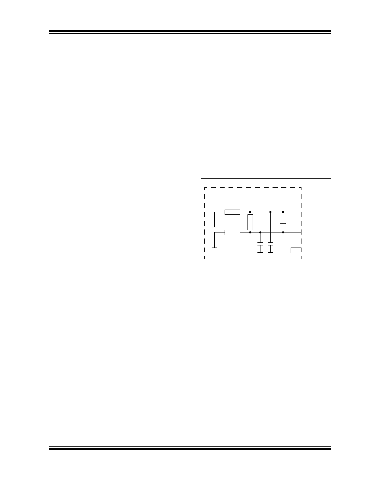
1.8
Typical Applications
In order to meet the EMC/EMI requirements, a
Common Mode Choke (CMC) might be required for
data rates greater than 1 Mbps.
FIGURE 1-1:
MCP2561FD WITH SPLIT PIN
FIGURE 1-2:
MCP2562FD WITH V
IO
PIN
5V LDO
V
DD
V
DD
T
XD
R
XD
STBY
CANTX
CANRX
RBX
V
SS
V
SS
PIC
®
MCU
MCP
256
1FD
SPLIT
CANH
CANL
4700 pF
0.1 μF
CANH
CANL
60
60
300
Optional
(
1
)
V
BAT
Note 1: Optional resistor to allow communication during bus failure (CANL shorted to ground).
1.8V LDO
V
DD
V
DD
T
XD
R
XD
STBY
CANTX
CANRX
RBX
V
SS
Vss
PIC
®
MCU
MCP
2562
FD
CANH
CANL
5V LDO
V
IO
0.1 μF
CANH
CANL
0.1 μF
120
V
BAT
2014 Microchip Technology Inc.
DS20005284A-page 7
MCP2561/2FD
2.0
ELECTRICAL
CHARACTERISTICS
2.1
Terms and Definitions
A number of terms are defined in ISO-11898 that are
used to describe the electrical characteristics of a CAN
transceiver device. These terms and definitions are
summarized in this section.
2.1.1
BUS VOLTAGE
V
CANL
and V
CANH
denote the voltages of the bus line
wires CANL and CANH relative to ground of each
individual CAN node.
2.1.2
COMMON MODE BUS VOLTAGE
RANGE
Boundary voltage levels of V
CANL
and V
CANH
with
respect to ground, for which proper operation will occur,
if up to the maximum number of CAN nodes are
connected to the bus.
2.1.3
DIFFERENTIAL INTERNAL
CAPACITANCE, C
DIFF
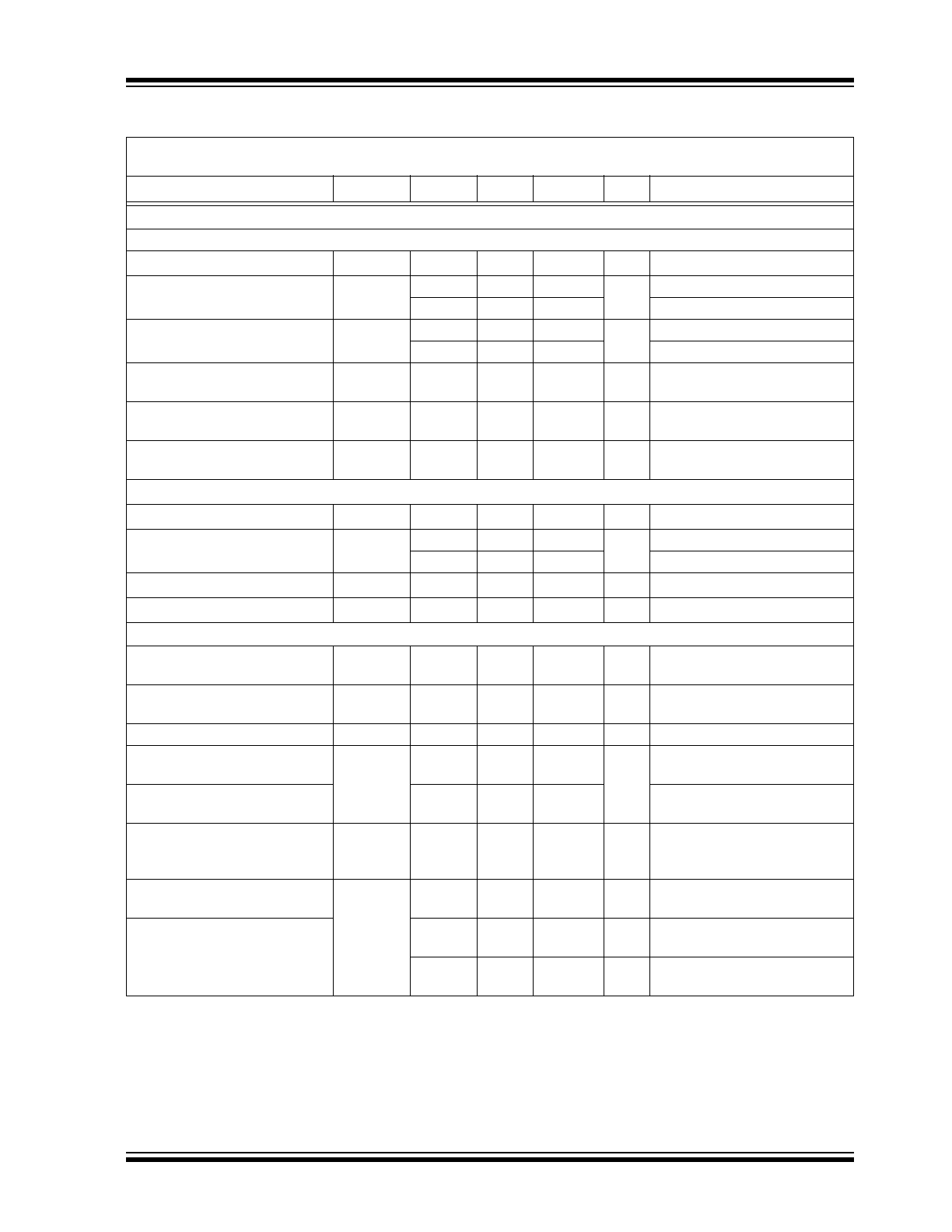
(OF A CAN NODE)
Capacitance seen between CANL and CANH during
the Recessive state, when the CAN node is
disconnected from the bus (see Figure 2-1).
2.1.4
DIFFERENTIAL INTERNAL
RESISTANCE, R
DIFF
(OF A CAN NODE)
Resistance seen between CANL and CANH during the
Recessive state when the CAN node is disconnected
from the bus (see Figure 2-1).
2.1.5
DIFFERENTIAL VOLTAGE, V
DIFF
(OF CAN BUS)
Differential voltage of the two-wire CAN bus, value
V
DIFF
= V
CANH
– V
CANL
.
2.1.6
INTERNAL CAPACITANCE, C
IN
(OF A CAN NODE)
Capacitance seen between CANL (or CANH) and
ground during the Recessive state, when the CAN
node is disconnected from the bus (see Figure 2-1).
2.1.7
INTERNAL RESISTANCE, R
IN
(OF A CAN NODE)
Resistance seen between CANL (or CANH) and
ground during the Recessive state, when the CAN
node is disconnected from the bus (see Figure 2-1).
FIGURE 2-1:
PHYSICAL LAYER
DEFINITIONS
R
IN
R
IN
R
DIFF
C
IN
C
IN
C
DIFF
CANL
CANH
GROUND
ECU

MCP2561/2FD
DS20005284A-page 8
2014 Microchip Technology Inc.
2.2
Absolute Maximum Ratings†
V
DD
.............................................................................................................................................................................7.0V
V
IO
..............................................................................................................................................................................7.0V
DC Voltage at T
XD
, R
XD
, STBY and V
SS
.............................................................................................-0.3V to V
IO
+ 0.3V
DC Voltage at CANH, CANL and SPLIT ...................................................................................................... -58V to +58V
Transient Voltage on CANH, CANL (ISO-7637) (See Figure 2-5)............................................................ -150V to +100V
Storage temperature ...............................................................................................................................-55°C to +150°C
Operating ambient temperature ..............................................................................................................-40°C to +150°C
Virtual Junction Temperature, T
VJ
(IEC60747-1) ....................................................................................-40°C to +190°C
Soldering temperature of leads (10 seconds) .......................................................................................................+300°C
ESD protection on CANH and CANL pins for MCP2561FD (IEC 61000-4-2) ........................................................±14 kV
ESD protection on CANH and CANL pins for MCP2562FD (IEC 61000-4-2) ..........................................................±8 kV
ESD protection on CANH and CANL pins (IEC 801; Human Body Model)..............................................................±8 kV
ESD protection on all other pins (IEC 801; Human Body Model).............................................................................±4 kV
ESD protection on all pins (IEC 801; Machine Model) ............................................................................................±300V
ESD protection on all pins (IEC 801; Charge Device Model)..................................................................................±750V
† NOTICE: Stresses above those listed under “Maximum ratings” may cause permanent damage to the device. This
is a stress rating only and functional operation of the device at those or any other conditions above those indicated in
the operational listings of this specification is not implied. Exposure to maximum rating conditions for extended periods
may affect device reliability.
2014 Microchip Technology Inc.
DS20005284A-page 9
MCP2561/2FD
2.3
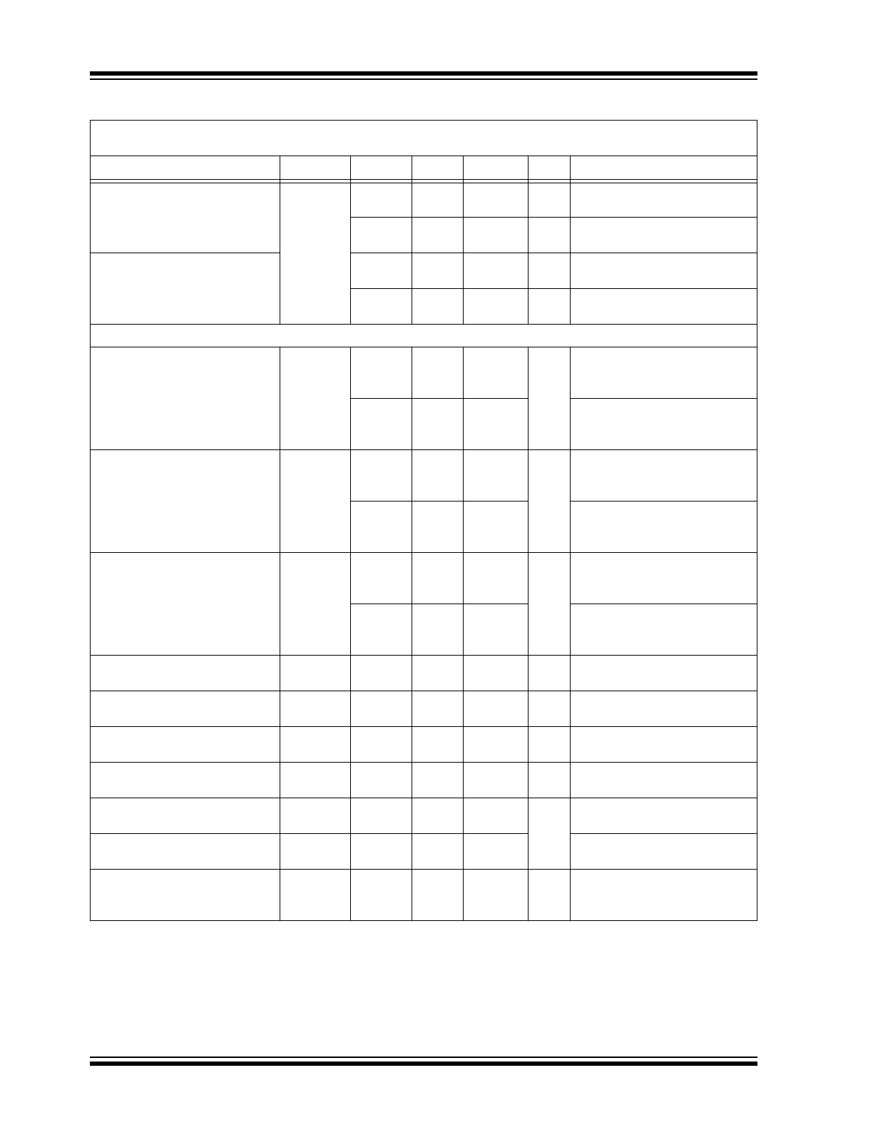
DC Characteristics
Electrical Characteristics: Extended (E): T
AMB
= -40°C to +125°C and High (H): T
AMB
= -40°C to +150°C;
V
DD
= 4.5V to 5.5V, V
IO
= 1.8V to 5.5V (Note 2), R
L
= 60
, C
L
= 100 pF; unless otherwise specified.
Characteristic
Sym
Min
Typ
Max
Units
Conditions
SUPPLY
V
DD
Pin
Voltage Range
V
DD
4.5
—
5.5
Supply Current
I
DD
—
5
10
mA
Recessive; V
TXD
= V
DD
—
45
70
Dominant; V
TXD
= 0V
Standby Current
I
DDS
—
5
15
µA
MCP2561FD
—
5
15
MCP2562FD; Includes I
IO
High Level of the POR
Comparator
V
PORH
3.8
—
4.3
V
Low Level of the POR
Comparator
V
PORL
3.4
—
4.0
V
Hysteresis of POR
Comparator
V
PORD
0.3
—
0.8
V
V
IO
Pin
Digital Supply Voltage Range
V
IO
1.8
—
5.5
V
Supply Current on V
IO
I
IO
—
4
30
µA
Recessive; V
TXD
= V
IO
—
85
500
Dominant; V
TXD
= 0V
Standby Current
I
DDS
—
0.3
1
µA
(Note 1)
Undervoltage detection on V
IO
V
UVD
(
IO
)
—
1.2
—
V
(Note 1)
BUS LINE (CANH; CANL) TRANSMITTER
CANH; CANL:
Recessive Bus Output Voltage
V
O
(
R
)
2.0
0.5V
DD
3.0
V
V
TXD
= V
DD
; No load
CANH; CANL:
Bus Output Voltage in Standby
V
O
(
S
)
-0.1
0.0
+0.1
V
STBY = V
TXD
= V
DD
; No load
Recessive Output Current
I
O
(
R
)
-5
—
+5
mA
-24V < V
CAN
< +24V
CANH: Dominant
Output Voltage
V
O
(
D
)
2.75
3.50
4.50
V
T
XD
= 0; R
L
= 50 to 65
CANL: Dominant
Output Voltage
0.50
1.50
2.25
R
L
= 50 to 65
Symmetry of Dominant
Output Voltage
(V
DD
– V
CANH
– V
CANL
)
V
O
(
D
)(
M
)
-400
0
+400
mV
V
TXD
= V
SS
(Note 1)
Dominant: Differential
Output Voltage
V
O
(
DIFF
)
1.5
2.0
3.0
V
V
TXD
= V
SS
; R
L
= 50 to 65
Figure 2-2, Figure 2-4
Recessive:
Differential Output Voltage
-120
0
12
mV
V
TXD
= V
DD
Figure 2-2, Figure 2-4
-500
0
50
mV
V
TXD
= V
DD,
no load.
Figure 2-2, Figure 2-4
Note 1:
Characterized; not 100% tested.
2:
Only MCP2562FD has V
IO
pin. For the MCP2561FD, V
IO
is internally connected to V
DD
.
3:
-12V to 12V is ensured by characterization, tested from -2V to 7V.
MCP2561/2FD
DS20005284A-page 10
2014 Microchip Technology Inc.
CANH: Short Circuit
Output Current
I
O
(
SC
)
-120
85
—
mA
V
TXD
= V
SS
; V
CANH
= 0V;
CANL: floating
-100
—
—
mA
same as above, but
V
DD
=5V, T
AMB
= 25°C (Note 1)
CANL: Short Circuit
Output Current
—
75
+120
mA
V
TXD
= V
SS
; V
CANL
= 18V;
CANH: floating
—
—
+100
mA
same as above, but
V
DD
=5V, T
AMB
= 25°C (Note 1)
BUS LINE (CANH; CANL) RECEIVER
Recessive Differential
Input Voltage
V
DIFF
(
R
)(
I
)
-1.0
—
+0.5
V
Normal Mode;
-12V < V(
CANH
,
CANL
) < +12V;
See Figure 2-6 (Note 3)
-1.0
—
+0.4
Standby Mode;
-12V < V(
CANH
,
CANL
) < +12V;
See Figure 2-6 (Note 3)
Dominant Differential
Input Voltage
V
DIFF
(
D
)(
I
)
0.9
—
V
DD
V
Normal Mode;
-12V < V(
CANH
,
CANL
) < +12V;
See Figure 2-6 (Note 3)
1.0
—
V
DD
Standby Mode;
-12V < V(
CANH
,
CANL
) < +12V;
See Figure 2-6 (Note 3)
Differential
Receiver Threshold
V
TH
(
DIFF
)
0.5
0.7
0.9
V
Normal Mode;
-12V < V(
CANH
,
CANL
) < +12V;
See Figure 2-6 (Note 3)
0.4
—
1.15
Standby Mode;
-12V < V(
CANH
,
CANL
) < +12V;
See Figure 2-6 (Note 3)
Differential
Input Hysteresis
V
HYS
(
DIFF
)
50
—
200
mV
Normal mode, see Figure 2-6,
(Note 1)
Common Mode
Input Resistance
R
IN
10
—
30
k
(Note 1)
Common Mode
Resistance Matching
R
IN
(
M
)
-1
0
+1
%
V
CANH
= V
CANL
, (Note 1)
Differential Input
Resistance
R
IN
(
DIFF
)
10
—
100
k
(Note 1)
Common Mode
Input Capacitance
C
IN
(
CM
)
—
—
20
pF
V
TXD
= V
DD
; (Note 1)
Differential
Input Capacitance
C
IN
(
DIFF
)
—
—
10
V
TXD
= V
DD
; (Note 1)
CANH, CANL:
Input Leakage
I
LI
-5
—
+5
µA
V
DD
= V
TXD
= V
STBY
= 0V.
For MCP2562FD, V
IO
= 0V.
V
CANH
= V
CANL
= 5 V.
2.3
DC Characteristics (Continued)
Electrical Characteristics: Extended (E): T
AMB
= -40°C to +125°C and High (H): T
AMB
= -40°C to +150°C;
V
DD
= 4.5V to 5.5V, V
IO
= 1.8V to 5.5V (Note 2), R
L
= 60
, C
L
= 100 pF; unless otherwise specified.
Characteristic
Sym
Min
Typ
Max
Units
Conditions
Note 1:
Characterized; not 100% tested.
2:
Only MCP2562FD has V
IO
pin. For the MCP2561FD, V
IO
is internally connected to V
DD
.
3:
-12V to 12V is ensured by characterization, tested from -2V to 7V.