
2016 Microchip Technology Inc.
DS20005533A-page 1
MCP2557FD/8FD
Features
• Silent Mode is Useful in the Following
Applications:
- Disables transmitter in redundant systems
- Implements babbling idiot protection
- Tests connection of bus medium
- Prevents a faulty CAN controller from
disrupting all network communications
• Optimized for CAN FD at 2, 5 and 8 Mbps
Operation:
- Maximum propagation delay: 120 ns
- Loop delay symmetry: ±10%(2 Mbps)
• Meets or Exceeds Stringent Automotive Design
Requirements Including “Hardware Require-
ments for LIN, CAN and FlexRay Interfaces in
Automotive Applications”, Version 1.3, May 2012:
- Conducted emissions at 2 Mbps with
Common-Mode Choke (CMC)
- DPI at 2 Mbps with
CMC
• Meets SAE J2962/2 “Communication Transceiv-
ers Qualification Requirements – CAN”
- Passes radiated emissions at 2 Mbps without
a CMC
• Meets Latest ISO/DIS-11898-2:2015
• Meets Latest SAE J2284-4 and -5 Working Drafts
• Digital Inputs of the MCP2557FD are Compatible
to 3.3V and 5V Microcontrollers. R
XD
Output
Requires a 5V Tolerant Microcontroller Input
• Functional Behavior Predictable Under all Supply
Conditions:
- Device is in Unpowered mode if V
DD
drops
below Power-on Reset (POR) level
- Device is in Unpowered mode if V
IO
drops
below POR level
Applications
CAN 2.0 and CAN FD networks in Automotive,
Industrial, Aerospace, Medical, and Consumer
applications.
Description
The MCP2557FD/8FD CAN transceiver family is
designed for high-speed CAN FD applications with up
to 8 Mbps communication speed. The maximum prop-
agation delay was improved to support longer bus
length.
The device meets automotive requirements for CAN
FD bit rates exceeding 2 Mbps, low quiescent current,
electromagnetic compatibility (EMC) and electrostatic
discharge (ESD).
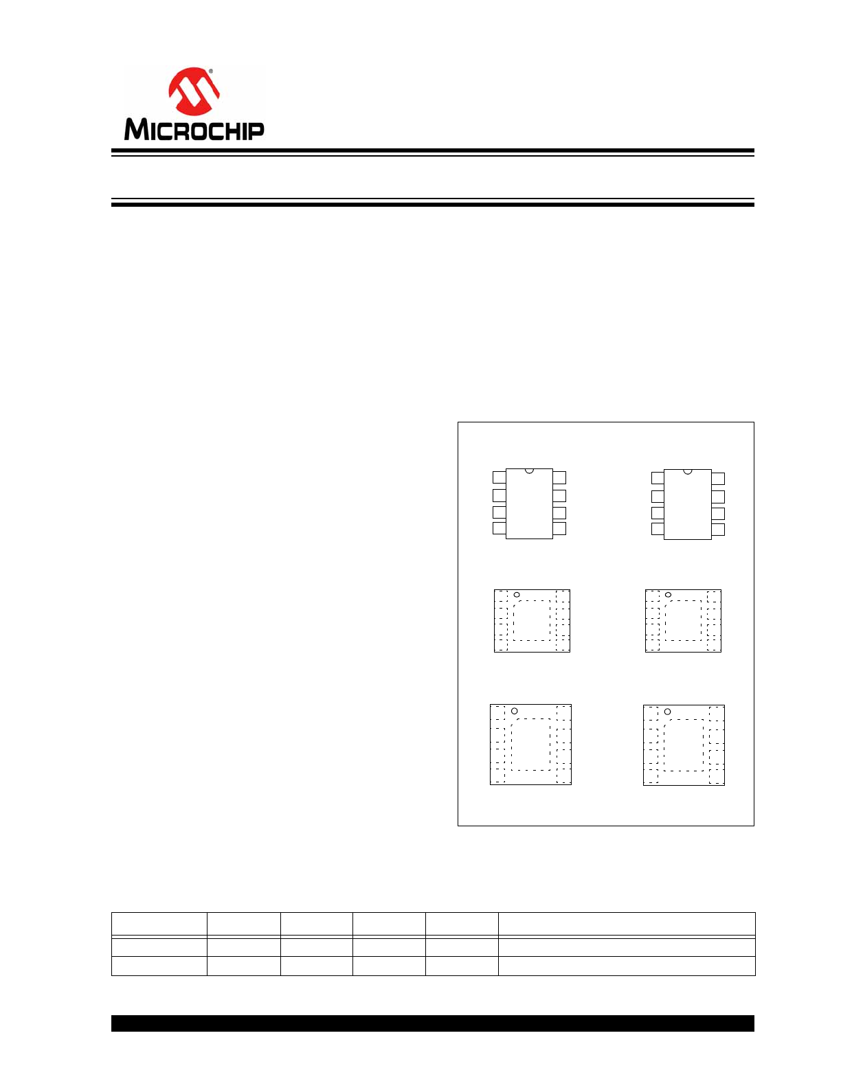
Package Types
MCP2557FD/8FD Family Members
MCP2558FD
SOIC
V
DD
V
SS
R
XD
CANH
CANL
1
2
3
4
8
7
6
5 V
IO
S
T
XD
MCP2557FD
SOIC
V
DD
V
SS
R
XD
CANH
CANL
NC
S
T
XD
MCP2557FD
2x3 TDFN*
MCP2558FD
2x3 TDFN*
V
DD
V
SS
R
XD
CANH
CANL
1
2
3
4
8
7
6
5 NC
S
T
XD
V
DD
V
SS
R
XD
CANH
CANL
V
IO
S
T
XD
MCP2558FD
3x3 DFN*
MCP2557FD
3x3 DFN*
V
DD
V
SS
R
XD
CANH
CANL
NC
S
T
XD
V
DD
V
SS
R
XD
CANH
CANL
V
IO
S
T
XD
1
2
3
4
8
7
6
5
EP
9
1
2
3
4
8
7
6
5
EP
9
1
2
3
4
8
7
6
5
EP
9
1
2
3
4
8
7
6
5
EP
9
*Includes Exposed Thermal Pad (EP); see
Table 1-1
.
Device
V
IO
Pin
NC
TTL I/O
V
IO
I/O
Description
MCP2557FD
N/A
Yes
Yes
N/A
—
MCP2558FD
Yes
N/A
N/A
Yes
Internal level shifter on digital I/O pins.
Note:
For ordering information, see the
Product Identification System
section.
CAN FD Transceiver with Silent Mode
MCP2557FD/8FD
DS20005533A-page 2
2016 Microchip Technology Inc.
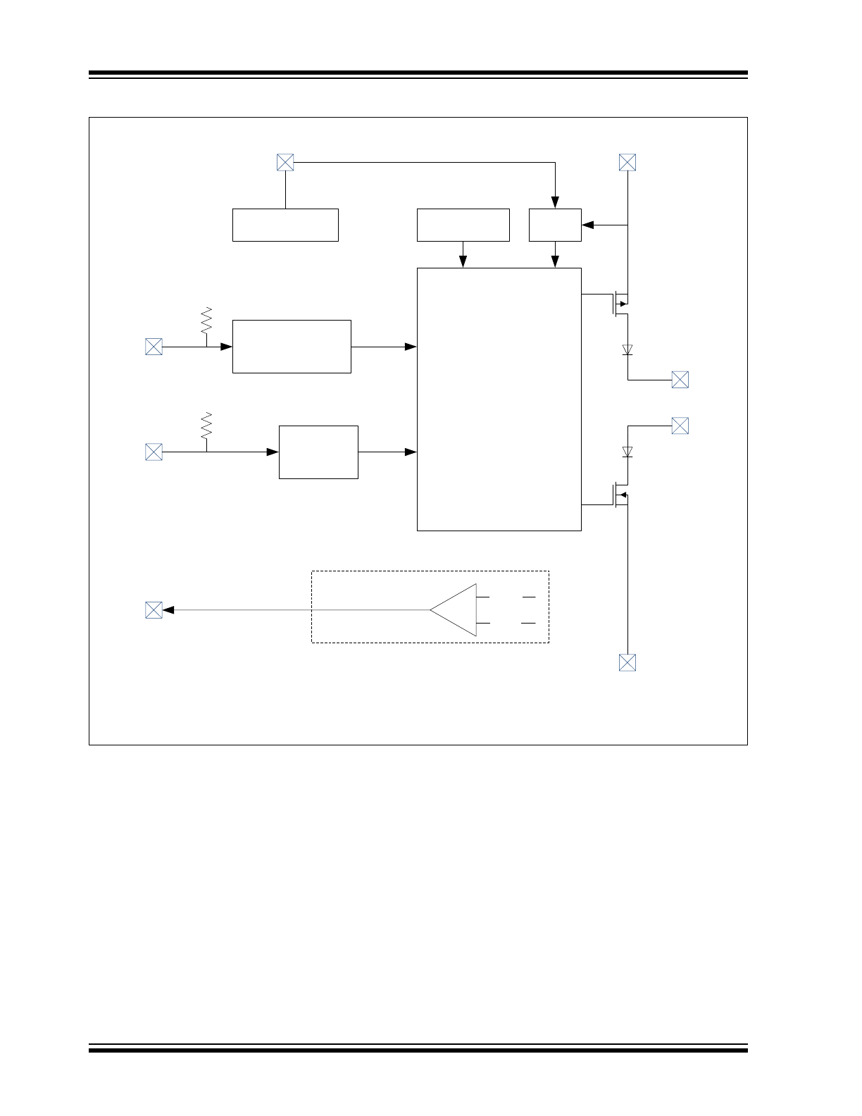
Block Diagram
Note:
Only the MCP2558FD has the V
IO
pin. In the MCP2557FD, the supply for the digital I/O is internally
connected to V
DD
.
V
DD
CANH
CANL
T
XD
R
XD
DRIVER
AND
SLOPE CONTROL
THERMAL
PROTECTION
POR
UVLO
DIGITAL I/O
SUPPLY
V
IO
V
SS
S
PERMANENT
DOMINANT DETECT
V
IO
V
IO
MODE
CONTROL
CANH
CANL
HS_RX
V
DD

2016 Microchip Technology Inc.
DS20005533A-page 3
MCP2557FD/8FD
1.0
DEVICE OVERVIEW
The MCP2557FD/8FD CAN transceiver family is
designed for high-speed CAN FD applications with up
to 8 Mbps communication speed. The product offers a
Silent mode controlled by the Silent mode pin. The
Silent mode is used to disable the CAN transmitter.
This ensures that the device doesn’t drive the CAN
bus. The MCP2557FD/8FD device provides
differential transmit and receive capability for the CAN
protocol controller, and is fully compatible with
specification ISO/DIS-11898-2:2015.
The loop delay symmetry is tested to support data rates
that are up to 8 Mbps for CAN FD (Flexible Data rate).
The maximum propagation delay was improved to
support longer bus length.
Typically, each node in a CAN system must have a
device convert the digital signals generated by a CAN
controller to signals suitable for transmission over the
bus cabling (differential output). It also provides a buffer
between the CAN controller and the high-voltage
spikes that can be generated on the CAN bus by
outside sources.
1.1
Transmitter Function
The CAN bus has two states: Dominant and
Recessive. A Dominant state occurs when the
differential voltage between CANH and CANL is
greater than V
DIFF
(
D
)(
I
). A Recessive state occurs
when the differential voltage is less than V
DIFF
(
R
)(
I
).
The Dominant and Recessive states correspond to the
Low and High states of the T
XD
input pin, respectively.
However, a Dominant state initiated by another CAN
node will override a Recessive state on the CAN bus.
1.2
Receiver Function
The R
XD
output pin reflects the differential bus voltage
between CANH and CANL. The Low and High states of
the R
XD
output pin correspond to the Dominant and
Recessive states of the CAN bus, respectively.
1.3
Internal Protection
CANH and CANL are protected against battery short
circuits and electrical transients that can occur on the
CAN bus. This feature prevents destruction of the
transmitter output stage during such a fault condition.
The device is further protected from excessive current
loading by thermal shutdown circuitry that disables the
output drivers when the junction temperature exceeds
a nominal limit of +175°C.
All other parts of the chip remain operational, and the
chip temperature is lowered due to the decreased
power dissipation in the transmitter outputs. This
protection is essential to guard against bus line short-
circuit-induced damage. Thermal protection is only
active during Normal mode.
1.4
Permanent Dominant Detection
The MCP2557FD/8FD device prevents a permanent
dominant condition on T
XD
.
In Normal mode, if the MCP2557FD/8FD detects an
extended Low state on the T
XD
input, it will disable the
CANH and CANL output drivers in order to prevent
data corruption on the CAN bus. The drivers will remain
disabled until T
XD
goes High. The high-speed receiver
is active, and data on the CAN bus is received on R
XD
.
The condition has a time-out of 1.9 ms (typical). This
implies a maximum bit time of 128 µs (7.8 kHz),
allowing up to 18 consecutive dominant bits on the bus.
1.5
Power-on Reset (POR) and
Undervoltage Detection
The MCP2557FD/8FD have POR detection on both
supply pins, V
DD
and V
IO
. Typical POR thresholds to
deassert the reset are 1.2V and 3.0V for V
IO
and V
DD
,
respectively.
When the device is powered on, CANH and CANL
remain in a high-impedance state until V
DD
exceeds its
undervoltage level. Once powered on, CANH and
CANL will enter a high-impedance state if the voltage
level at V
DD
drops below the undervoltage level,
providing voltage brown-out protection during normal
operation.
The receiver output is forced to a Recessive state
during an undervoltage condition on V
DD
.

MCP2557FD/8FD
DS20005533A-page 4
2016 Microchip Technology Inc.
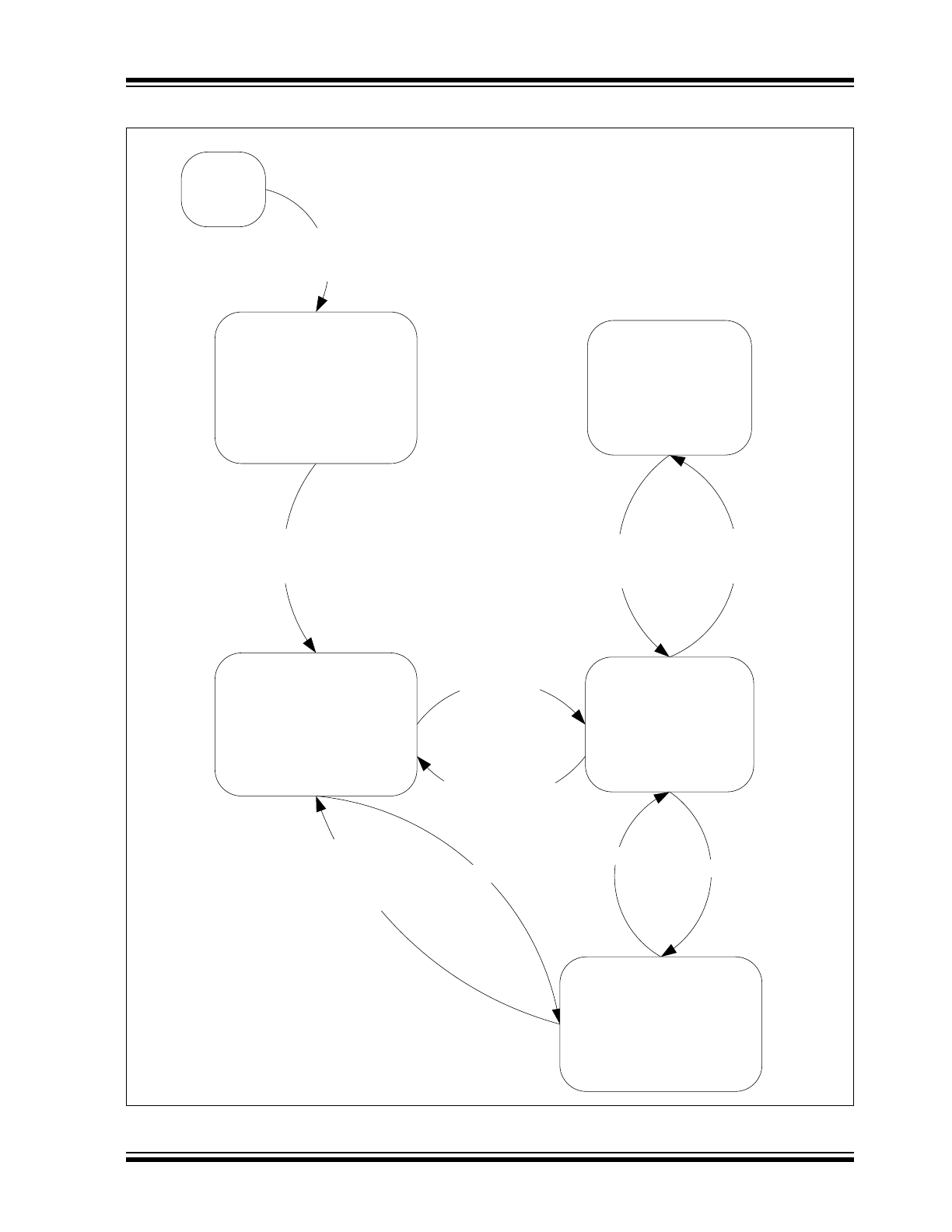
1.6
Mode Control
Figure 1-1
shows the state diagram of the MCP2557FD/
8FD.
1.6.1
UNPOWERED MODE (POR)
The MCP2557FD/8FD enters Unpowered mode if any
of the following conditions occur:
• After powering up the device
• If V
DD
drops below V
PORL
• If V
IO
drops below V
PORL
_V
IO
In Unpowered mode, the CAN bus will be biased to
ground using a high impedance. The MCP2557FD/
8FD is not able to communicate on the bus.
1.6.2
WAKE MODE
The MCP2557FD/8FD transitions from Unpowered
mode to Wake mode when V
DD
and V
IO
are above
their PORH levels. From Normal mode, if V
DD
is
smaller than V
UVL
, or if the bandgap output voltage is
not within valid range, the device will also enter Wake
mode.
In Wake mode, the CAN bus is biased to ground and
R
XD
is always high.
1.6.3
NORMAL MODE
When V
DD
exceeds V
UVH
, the band gap is within valid
range and T
XD
is High, the device transitions into
Normal mode. During POR, when the microcontroller
powers up, the T
XD
pin could be unintentionally pulled
down by the microcontroller powering up. To avoid
driving the bus during a POR of the microcontroller,
the transceiver proceeds to Normal mode only after
T
XD
is high.
In Normal mode, the driver block is operational and
can drive the bus pins. The slopes of the output
signals on CANH and CANL are optimized to reduce
Electromagnetic Emissions (EME). The CAN bus is
biased to V
DD
/2.
The high-speed differential receiver is active.
1.6.4
SILENT MODE
The device may be placed in Silent mode by applying
a high level to the ‘S’ pin (pin 8). In Silent mode, the
transmitter is disabled and the CAN bus is biased to
V
DD
/2. The high-speed differential receiver is active.
The CAN controller must put the MCP2557FD/8FD
back into Normal mode to enable the transmitter.
2016 Microchip Technology Inc.
DS20005533A-page 5
MCP2557FD/8FD
FIGURE 1-1:
MCP2557FD/8FD STATE DIAGRAM
SILENT High
Bandgap Not Ok
Or
V
DD
< V
UVL
And
Bandgap Not Ok
Or
V
DD
< V
UVL
TXD High
And
Bandgap ok
And
V
DD
> V
UVH
And
Silent Low
SILENT Low
SILENT High
T
XD
High
And
T < TJ(SD)-TJ(HYST)
T
XD
Low > Tpdt
Or
T > TJ(SD)
V
DD
< V
PORL
Or
V
IO
< V
PORL
_V
IO
V
DD
> V
PORH
And
V
IO
> V
PORH
_V
IO
Normal
CAN Driven
Common Mode V
DD
/2
HS RX ON
R
XD
= f(HS RX)
T
XD
Time-Out
CAN Recessive
Common Mode V
DD
/2
HS RX ON
R
XD
= f(HS RX)
UnPowered (POR)
CAN High Impedance
Common Mode Tied to
GND
HS RX OFF
R
XD
High
Bandgap OFF
From any
State
Wake
Start Bandgap
CAN High Impedance
Common Mode Tied to
GND
HS RX OFF
RXD High
Silent
CAN Recessive (TX OFF)
Common Mode V
DD
/2
HS RX ON
RX
D
= f(HS RX)
MCP2557FD/8FD
DS20005533A-page 6
2016 Microchip Technology Inc.
1.7
Pin Descriptions
The descriptions of the pins are listed in
Table 1-1
.
1.7.1
TRANSMITTER DATA
INPUT PIN (T
XD
)
The CAN transceiver drives the differential output pins
CANH and CANL according to T
XD
. It is usually
connected to the transmitter data output of the CAN
controller device. When T
XD
is Low, CANH and CANL
are in the Dominant state. When T
XD
is High, CANH
and CANL are in the Recessive state, provided that
another CAN node is not driving the CAN bus with a
Dominant state. T
XD
is connected from an internal pull-
up resistor (nominal 33 k
) to V
DD
or V
IO
, in the
MCP2557FD or MCP2558FD, respectively.
1.7.2
GROUND SUPPLY PIN (V
SS
)
Ground supply pin.
1.7.3
SUPPLY VOLTAGE PIN (V
DD
)
Positive supply voltage pin. Supplies transmitter and
receiver.
1.7.4
RECEIVER DATA OUTPUT PIN (R
XD
)
R
XD
is a CMOS-compatible output that drives High or
Low depending on the differential signals on the CANH
and CANL pins, and is usually connected to the
receiver data input of the CAN controller device. R
XD
is
High when the CAN bus is Recessive, and Low in the
Dominant state. R
XD
is supplied by V
DD
or V
IO
, in the
MCP2557FD or MCP2558FD, respectively.
1.7.5
NC PIN (MCP2557FD)
No Connect. This pin can be left open or connected to
V
SS
.
1.7.6
V
IO
PIN (MCP2557FD)
Supply for digital I/O pins. In the MCP2557FD, the
supply for the digital I/O (T
XD
, R
XD
and S) is internally
connected to V
DD
.
1.7.7
DIGITAL I/O
The MCP2557FD/8FD enable easy interfacing to
MCUs with I/O ranges from 1.8V to 5V.
1.7.7.1
MCP2557FD
The V
IH
(
MIN
) and V
IL
(
MAX
) for T
XD
are independent of
V
DD
. They are set at levels that are compatible with 3V
and 5V microcontrollers.
The R
XD
pin is always driven to V
DD
; therefore, a 3V
microcontroller will need a 5V tolerant input.
1.7.7.2
MCP2558FD
V
IH
and V
IL
for S and T
XD
depend on V
IO
. The R
XD
pin
is driven to V
IO
.
1.7.8
CAN LOW PIN (CANL)
The CANL output drives the Low side of the CAN
differential bus. This pin is also tied internally to the
receive input comparator. CANL disconnects from the
bus when the MCP2557FD/8FD devices are not
powered.
1.7.9
CAN HIGH PIN (CANH)
The CANH output drives the high side of the CAN
differential bus. This pin is also tied internally to the
receive input comparator. CANH disconnects from the
bus when the MCP2557FD/8FD devices are not
powered.
TABLE 1-1:
MCP2557FD/8FD PIN DESCRIPTIONS
MCP2557FD
3 x 3 DFN,
2 x 3 TDFN
MCP2557FD
SOIC
MCP2558FD
3 x 3 DFN,
2 x 3 TDFN
MCP2558FD
SOIC
Symbol
Pin Function
1
1
1
1
T
XD
Transmit Data Input
2
2
2
2
V
SS
Ground
3
3
3
3
V
DD
Supply Voltage
4
4
4
4
R
XD
Receive Data Output
5
5
—
—
NC
No Connect (MCP2557FD only)
—
—
5
5
V
IO
Digital I/O Supply Pin
(MCP2558FD only)
6
6
6
6
CANL
CAN Low-Level Voltage I/O
7
7
7
7
CANH
CAN High-Level Voltage I/O
8
8
8
8
S
Silent Mode Input
9
—
9
—
EP
Exposed Thermal Pad

2016 Microchip Technology Inc.
DS20005533A-page 7
MCP2557FD/8FD
1.7.10
SILENT MODE INPUT PIN (S)
This pin sets Normal or Silent mode. In Silent mode, the
transmitter is off and the high-speed receiver is active.
The CAN bus common mode voltage is V
DD
/2 when in
Silent mode.
The ‘S’ pin (pin 8) is connected to an internal MOS pull-
up resistor to V
DD
or V
IO
, in the MCP2557FD or
MCP2558FD, respectively. The value of the MOS pull-
up resistor depends on the supply voltage. Typical val-
ues are 660 k
for 5V, 1.1 M for 3.3V and 4.4 M for
1.8V
1.7.11
EXPOSED THERMAL PAD (EP)
It is recommended to connect this pad to V
SS
to
enhance electromagnetic immunity and thermal
resistance.
MCP2557FD/8FD
DS20005533A-page 8
2016 Microchip Technology Inc.
1.8
TYPICAL APPLICATION
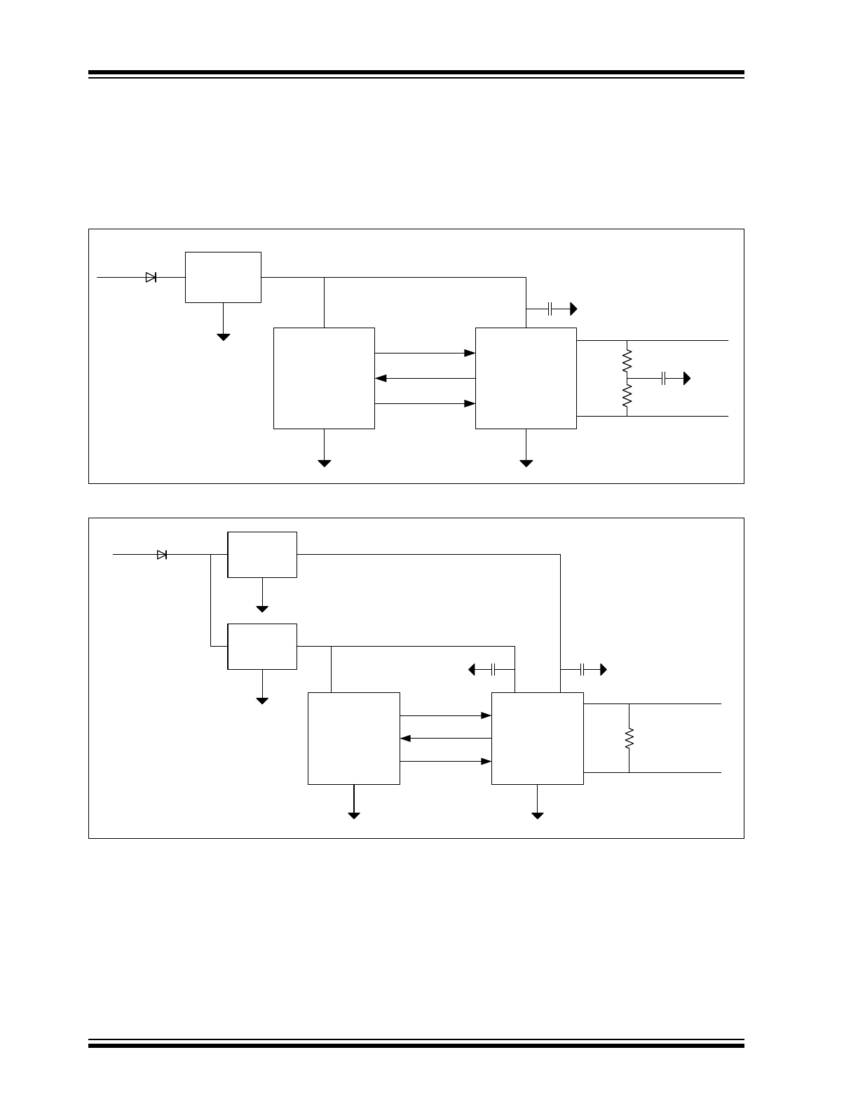
Figure 1-2
shows a typical application for the
MCP2557FD with the NC pin and a split termination.
Figure 1-3
illustrates a typical application for the
MCP2558FD.
FIGURE 1-2:
MCP2557FD WITH NC AND SPLIT TERMINATION
FIGURE 1-3:
MCP2558FD WITH V
IO
PIN
5V LDO
V
BAT
V
DD
V
DD
T
XD
R
XD
S
CANTX
CANRX
RBX
V
SS
V
SS
PIC
®
MC
U
MC
P
2
5
5
7
F
D
NC
CANH
CANL
0.1 μF
CANH
CANL
4700 pF
60
60
3.3V LDO
V
DD
V
DD
T
XD
R
XD
S
CANTX
CANRX
RBX
V
SS
V
SS
PIC
®
MC
U
MC
P
2
5
5
8
F
D
CANH
CANL
5V LDO
V
BAT
V
IO
0.1 µF
0.1 µF
CANH
CANL
120
2016 Microchip Technology Inc.
DS20005533A-page 9
MCP2557FD/8FD
2.0
ELECTRICAL
CHARACTERISTICS
2.1
Terms and Definitions
A number of terms are defined in ISO/DIS-11898 that
are used to describe the electrical characteristics of a
CAN transceiver device. These terms and definitions
are summarized in this section.
2.1.1
BUS VOLTAGE
V
CANL
and V
CANH
denote the voltages of the bus line
wires CANL and CANH relative to the ground of each
individual CAN node.
2.1.2
COMMON MODE BUS VOLTAGE
RANGE
Boundary voltage levels of V
CANL
and V
CANH
with
respect to ground, for which proper operation will occur,
if the maximum number of CAN nodes are connected
to the bus.
2.1.3
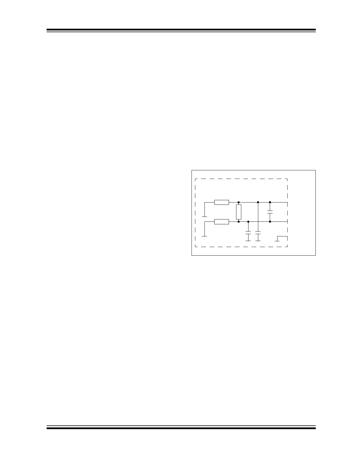
DIFFERENTIAL INTERNAL
CAPACITANCE, C
DIFF
(OF A CAN NODE)
Capacitance seen between CANL and CANH during
the Recessive state when the CAN node is
disconnected from the bus (see
Figure 2-1
).
2.1.4
DIFFERENTIAL INTERNAL
RESISTANCE, R
DIFF
(OF A CAN NODE)
Resistance seen between CANL and CANH during the
Recessive state when the CAN node is disconnected
from the bus (see
Figure 2-1
).
2.1.5
DIFFERENTIAL VOLTAGE, V
DIFF
(OF CAN BUS)
Differential voltage of the two-wire CAN bus, with value
equal to V
DIFF
= V
CANH
– V
CANL
.
2.1.6
INTERNAL CAPACITANCE, C
IN
(OF A CAN NODE)
Capacitance seen between CANL (or CANH) and
ground during the Recessive state when the CAN node
is disconnected from the bus (see
Figure 2-1
).
2.1.7
INTERNAL RESISTANCE, R
IN
(OF A CAN NODE)
Resistance seen between CANL (or CANH) and
ground during the Recessive state when the CAN node
is disconnected from the bus (see
Figure 2-1
).
FIGURE 2-1:
PHYSICAL LAYER
DEFINITIONS
R
IN
R
IN
R
DIFF
C
IN
C
IN
C
DIFF
CANL
CANH
GROUND
ECU

MCP2557FD/8FD
DS20005533A-page 10
2016 Microchip Technology Inc.
2.2
Absolute Maximum Ratings†
V
DD
.............................................................................................................................................................................7.0V
V
IO
..............................................................................................................................................................................7.0V
DC Voltage at T
XD
, R
XD
, S and V
SS
....................................................................................................-0.3V to V
IO
+ 0.3V
DC Voltage at CANH, and CANL ................................................................................................................. -58V to +58V
Transient Voltage on CANH, and CANL (ISO/DIS-7637) (
Figure 2-5
) ..................................................... -150V to +100V
Differential Bus Input Voltage V
DIFF
(I) (t = 60 days, continuous)....................................................................-5V to +10V
Differential Bus Input Voltage V
DIFF
(I) (1000 pulses, t = 0.1 ms, V
CANH
= +18V).....................................................+17V
Dominant State Detection V
DIFF
(I) (10000 pulses, t = 1 ms).......................................................................................+9V
Storage temperature ...............................................................................................................................-55°C to +150°C
Operating ambient temperature ..............................................................................................................-40°C to +150°C
Virtual Junction Temperature, T
VJ
(IEC60747-1) ....................................................................................-40°C to +190°C
Soldering temperature of leads (10 seconds) ....................................................................................................... +300°C
ESD protection on CANH and CANL pins (IEC 61000-4-2) ................................................................................... ±13 kV
ESD protection on CANH and CANL pins (IEC 801; Human Body Model).............................................................. ±8 kV
ESD protection on all other pins (IEC 801; Human Body Model)............................................................................. ±4 kV
ESD protection on all pins (IEC 801; Machine Model) ............................................................................................±400V
ESD protection on all pins (IEC 801; Charge Device Model) ..................................................................................±750V
† Notice: Stresses above those listed under “Maximum ratings” may cause permanent damage to the device. This is
a stress rating only and functional operation of the device at those or any other conditions above those indicated in
the operational listings of this specification is not implied. Exposure to maximum rating conditions for extended periods
may affect device reliability.