
2001-2016 Microchip Technology Inc.
DS20001667G-page 1
MCP2551
Features
• Supports 1 Mb/s operation
• Implements ISO-11898 standard physical layer
requirements
• Suitable for 12V and 24V systems
• Externally-controlled slope for reduced RFI
emissions
• Detection of ground fault (permanent Dominant)
on TXD input
• Power-on Reset and voltage brown-out protection
• An unpowered node or brown-out event will not
disturb the CAN bus
• Low current standby operation
• Protection against damage due to short-circuit
conditions (positive or negative battery voltage)
• Protection against high-voltage transients
• Automatic thermal shutdown protection
• Up to 112 nodes can be connected
• High-noise immunity due to differential bus
implementation
• Temperature ranges:
- Industrial (I): -40°C to +85°C
- Extended (E): -40°C to +125°C
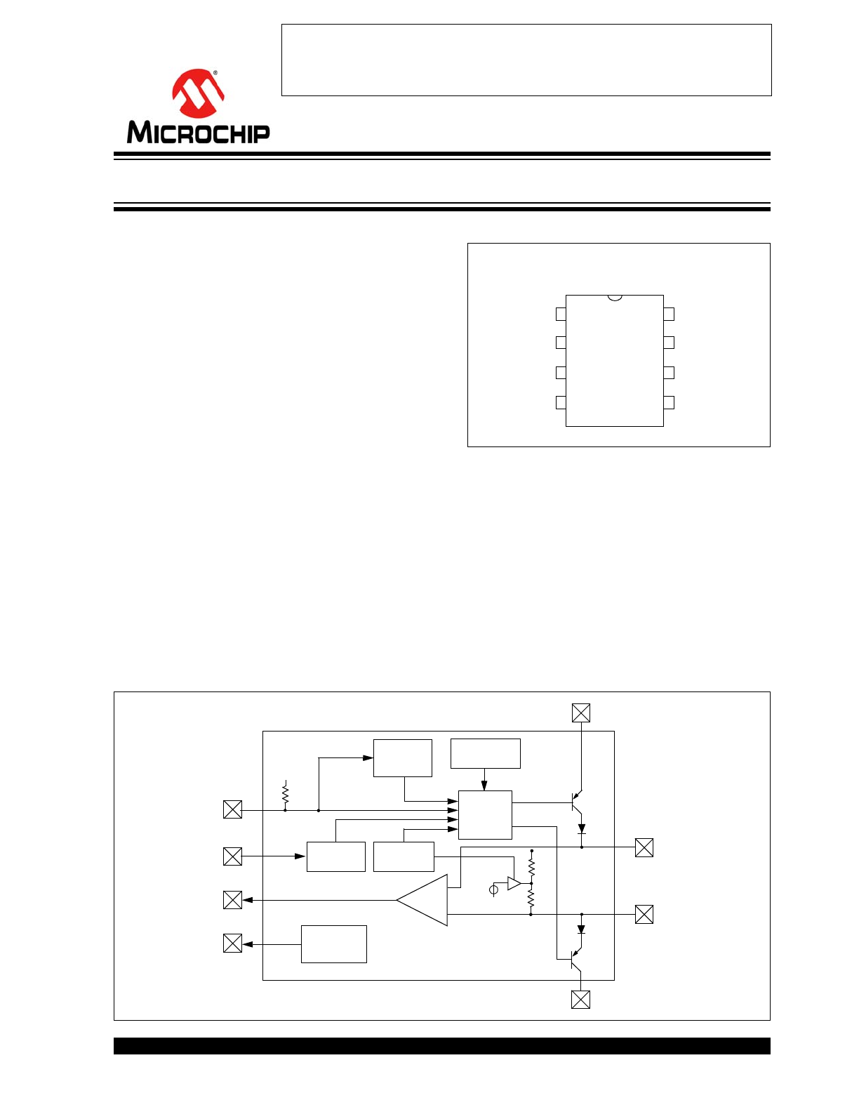
Package Types
Block Diagram
R
S
CANH
CANL
V
REF
TXD
V
SS
V
DD
RXD
1
2
3
4
8
7
6
5
PDIP/SOIC
MCP
255
1
Thermal
Shutdown
V
DD
V
SS
CANH
CANL
TXD
R
S
RXD
V
REF
V
DD
Slope
Control
Power-On
Reset
Reference
Voltage
Receiver
GND
0.5 V
DD
TXD
Dominant
Detect
Driver
Control
High-Speed CAN Transceiver
Not Recommended for New Designs
Please use MCP2561

MCP2551
DS20001667G-page 2
2001-2016 Microchip Technology Inc.
NOTES:

2001-2016 Microchip Technology Inc.
DS20001667G-page 3
MCP2551
1.0
DEVICE OVERVIEW
The MCP2551 is a high-speed CAN, fault-tolerant
device that serves as the interface between a CAN
protocol controller and the physical bus. The MCP2551
device provides differential transmit and receive
capability for the CAN protocol controller, and is fully
compatible with the ISO-11898 standard, including 24V
requirements. It will operate at speeds of up to 1 Mb/s.
Typically, each node in a CAN system must have a
device to convert the digital signals generated by a
CAN controller to signals suitable for transmission over
the bus cabling (differential output). It also provides a
buffer between the CAN controller and the high-voltage
spikes that can be generated on the CAN bus by
outside sources (EMI, ESD, electrical transients, etc.).
1.1
Transmitter Function
The CAN bus has two states: Dominant and
Recessive. A Dominant state occurs when the
differential voltage between CANH and CANL is
greater than a defined voltage (e.g.,1.2V). A Recessive
state occurs when the differential voltage is less than a
defined voltage (typically 0V). The Dominant and
Recessive states correspond to the Low and High state
of the TXD input pin, respectively. However, a
Dominant state initiated by another CAN node will
override a Recessive state on the CAN bus.
1.1.1
MAXIMUM NUMBER OF NODES
The MCP2551 CAN outputs will drive a minimum load
of 45
,
allowing a maximum of 112 nodes to be
connected (given a minimum differential input
resistance of 20 k
and a nominal termination resistor
value of 120
1.2
Receiver Function
The RXD output pin reflects the differential bus voltage
between CANH and CANL. The Low and High states of
the RXD output pin correspond to the Dominant and
Recessive states of the CAN bus, respectively.
1.3
Internal Protection
CANH and CANL are protected against battery short
circuits and electrical transients that can occur on the
CAN bus. This feature prevents destruction of the
transmitter output stage during such a fault condition.
The device is further protected from excessive current
loading by thermal shutdown circuitry that disables the
output drivers when the junction temperature exceeds
a nominal limit of 165°C. All other parts of the chip
remain operational, and the chip temperature is low-
ered due to the decreased power dissipation in the
transmitter outputs. This protection is essential to
protect against bus line short-circuit-induced damage.
1.4
Operating Modes
The R
S
pin allows three modes of operation to be
selected:
• High-Speed
• Slope-Control
• Standby
These modes are summarized in
Table 1-1
.
When in High-Speed or Slope-Control mode, the
drivers for the CANH and CANL signals are internally
regulated to provide controlled symmetry in order to
minimize EMI emissions.
Additionally, the slope of the signal transitions on
CANH and CANL can be controlled with a resistor
connected from pin 8 (R
S
) to ground. The slope must
be proportional to the current output at R
S
, which will
further reduce EMI emissions.
1.4.1
HIGH-SPEED
High-Speed mode is selected by connecting the R
S
pin
to V
SS
. In this mode, the transmitter output drivers have
fast output rise and fall times to support high-speed
CAN bus rates.
1.4.2
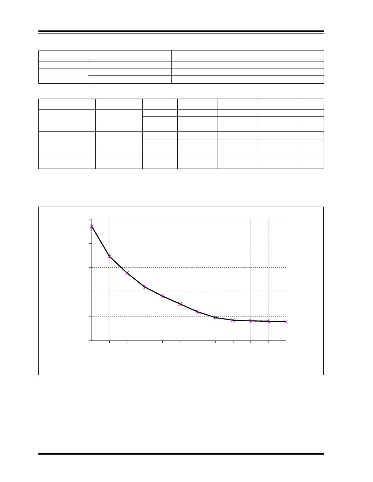
SLOPE-CONTROL
Slope-Control mode further reduces EMI by limiting the
rise and fall times of CANH and CANL. The slope, or
slew rate (SR), is controlled by connecting an external
resistor (R
EXT
) between R
S
and V
OL
(usually ground).
The slope is proportional to the current output at the R
S
pin. Since the current is primarily determined by the
slope-control resistance value R
EXT
, a certain slew rate
is achieved by applying a specific resistance.
Figure 1-1
illustrates typical slew rate values as a
function of the slope-control resistance value.
1.4.3
STANDBY MODE
The device may be placed in Standby or SLEEP mode
by applying a high-level to the R
S
pin. In SLEEP mode,
the transmitter is switched off and the receiver operates
at a lower current. The receive pin on the controller side
(RXD) is still functional, but will operate at a slower
rate. The attached microcontroller can monitor RXD for
CAN bus activity and place the transceiver into normal
operation via the R
S
pin (at higher bus rates, the first
CAN message may be lost).
MCP2551
DS20001667G-page 4
2001-2016 Microchip Technology Inc.
TABLE 1-1:
MODES OF OPERATION
TABLE 1-2:
TRANSCEIVER TRUTH TABLE
FIGURE 1-1:
SLEW RATE VS. SLOPE-CONTROL RESISTANCE VALUE
Mode
Current at R
s
Pin
Resulting Voltage at R
S
Pin
Standby
-I
RS
< 10 µA
V
RS
> 0.75 V
DD
Slope-Control
10 µA < -I
RS
< 200 µA
0.4 V
DD
< V
RS
< 0.6 V
DD
High-Speed
-I
RS
< 610 µA
0 < V
RS
< 0.3V
DD
V
DD
V
RS
TXD
CANH
CANL
Bus State
(
1
)
R
XD
(
1
)
4.5V
V
DD
5.5V
V
RS
< 0.75 V
DD
0
HIGH
LOW
Dominant
0
1 or floating
Not Driven
Not Driven
Recessive
1
V
RS
> 0.75 V
DD
X
Not Driven
Not Driven
Recessive
1
V
POR
< V
DD
< 4.5V
(See
Note 3
)
V
RS
< 0.75 V
DD
0
HIGH
LOW
Dominant
0
1 or floating
Not Driven
Not Driven
Recessive
1
V
RS
> 0.75 V
DD
X
Not Driven
Not Driven
Recessive
1
0 < V
DD
< V
POR
X
X
Not Driven/
No Load
Not Driven/
No Load
High Impedance
X
Note 1:
If another bus node is transmitting a Dominant bit on the CAN bus, then RXD is a logic ‘0’.
2:
X = “don’t care”.
3:
Device drivers will function, although outputs are not ensured to meet the ISO-11898 specification.
0
5
10
15
20
25
10
20
30
40
49
60
70
76
90 100 110 120
Resistance (k)
Slew Rate V/μs
2001-2016 Microchip Technology Inc.
DS20001667G-page 5
MCP2551
1.5
TXD Permanent Dominant
Detection
If the MCP2551 detects an extended Low state on the
TXD input, it will disable the CANH and CANL output
drivers in order to prevent the corruption of data on the
CAN bus. The drivers are disabled if TXD is Low for
more than 1.25 ms (minimum). This implies a
maximum bit time of 62.5 µs (16 kb/s bus rate),
allowing up to 20 consecutive transmitted Dominant
bits during a multiple bit error and error frame scenario.
The drivers remain disabled as long as TXD remains
Low. A rising edge on TXD will reset the timer logic and
enable the CANH and CANL output drivers.
1.6
Power-on Reset
When the device is powered on, CANH and CANL
remain in a high-impedance state until V
DD
reaches the
voltage level V
PORH
. In addition, CANH and CANL will
remain in a high-impedance state if TXD is Low when
V
DD
reaches V
PORH
. CANH and CANL will become
active only after TXD is asserted High. Once powered
on, CANH and CANL will enter a high-impedance state
if the voltage level at V
DD
falls below V
PORL
, providing
voltage brown-out protection during normal operation.
1.7
Pin Descriptions
The 8-pin pinout is listed in
Table 1-3
.
TABLE 1-3:
MCP2551 PINOUT
1.7.1
TRANSMITTER DATA INPUT (TXD)
TXD is a TTL-compatible input pin. The data on this pin
is driven out on the CANH and CANL differential output
pins. It is usually connected to the transmitter data
output of the CAN controller device. When TXD is low,
CANH and CANL are in the Dominant state. When TXD
is high, CANH and CANL are in the Recessive state,
provided that another CAN node is not driving the CAN
bus with a Dominant state. TXD has an internal pull-up
resistor (nominal 25 k
to V
DD
).
1.7.2
GROUND SUPPLY (V
SS
)
Ground supply pin.
1.7.3
SUPPLY VOLTAGE (V
DD
)
Positive supply voltage pin.
1.7.4
RECEIVER DATA OUTPUT (RXD)
RXD is a CMOS-compatible output that drives high or
low depending on the differential signals on the CANH
and CANL pins and is usually connected to the receiver
data input of the CAN controller device. RXD is High
when the CAN bus is Recessive and Low in the
Dominant state.
1.7.5
REFERENCE VOLTAGE (V
REF
)
Reference Voltage Output (defined as V
DD
/2).
1.7.6
CAN LOW (CANL)
The CANL output drives the low side of the CAN
differential bus. This pin is also tied internally to the
receive input comparator.
1.7.7
CAN HIGH (CANH)
The CANH output drives the high side of the CAN
differential bus. This pin is also tied internally to the
receive input comparator.
1.7.8
SLOPE RESISTOR INPUT (R
S
)
The R
S
pin is used to select High-Speed, Slope-Control
or Standby modes via an external biasing resistor.
Pin
Number
Pin
Name
Pin Function
1
TXD
Transmit Data Input
2
V
SS
Ground
3
V
DD
Supply Voltage
4
RXD
Receive Data Output
5
V
REF
Reference Output Voltage
6
CANL
CAN Low-Level Voltage I/O
7
CANH
CAN High-Level Voltage I/O
8
R
S
Slope-Control Input

MCP2551
DS20001667G-page 6
2001-2016 Microchip Technology Inc.
NOTES:
2001-2016 Microchip Technology Inc.
DS20001667G-page 7
MCP2551
2.0
ELECTRICAL
CHARACTERISTICS
2.1
Terms and Definitions
A number of terms are defined in ISO-11898 that are
used to describe the electrical characteristics of a CAN
transceiver device. These terms and definitions are
summarized in this section.
2.1.1
BUS VOLTAGE
V
CANL
and V
CANH
denote the voltages of the bus line
wires CANL and CANH relative to ground of each
individual CAN node.
2.1.2
COMMON MODE BUS VOLTAGE
RANGE
Boundary voltage levels of V
CANL
and V
CANH
with
respect to ground, for which proper operation will occur,
if up to the maximum number of CAN nodes are
connected to the bus.
2.1.3
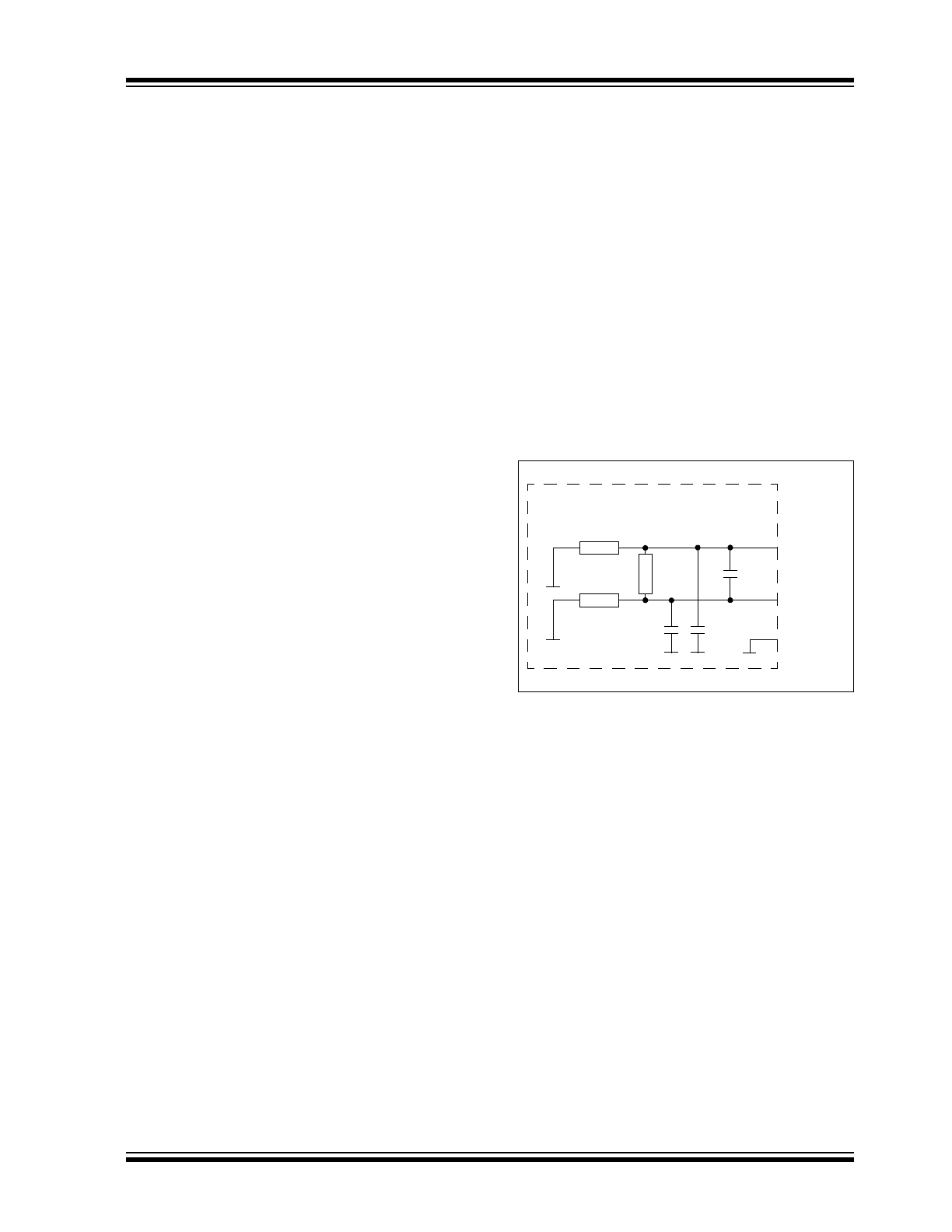
DIFFERENTIAL INTERNAL
CAPACITANCE, C
DIFF
(OF A CAN NODE)
Capacitance seen between CANL and CANH during
the Recessive state when the CAN node is
disconnected from the bus (see
Figure 2-1
).
2.1.4
DIFFERENTIAL INTERNAL
RESISTANCE, R
DIFF
(OF A CAN NODE)
Resistance seen between CANL and CANH during the
Recessive state when the CAN node is disconnected
from the bus (see
Figure 2-1
).
2.1.5
DIFFERENTIAL VOLTAGE, V
DIFF
(OF CAN BUS)
Differential voltage of the two-wire CAN bus, value
V
DIFF
= V
CANH
– V
CANL
.
2.1.6
INTERNAL CAPACITANCE, C
IN
(OF A CAN NODE)
Capacitance seen between CANL (or CANH) and
ground during the Recessive state when the CAN node
is disconnected from the bus (see
Figure 2-1
).
2.1.7
INTERNAL RESISTANCE, R
IN
(OF A CAN NODE)
Resistance seen between CANL (or CANH) and
ground during the Recessive state when the CAN node
is disconnected from the bus (see
Figure 2-1
).
FIGURE 2-1:
PHYSICAL LAYER
DEFINITIONS
R
IN
R
IN
R
DIFF
C
IN
C
IN
C
DIFF
CANL
CANH
GROUND
ECU

MCP2551
DS20001667G-page 8
2001-2016 Microchip Technology Inc.
Absolute Maximum Ratings†
V
DD
.............................................................................................................................................................................7.0V
DC Voltage at TXD, RXD, V
REF
and V
S
............................................................................................ -0.3V to V
DD
+ 0.3V
DC Voltage at CANH, CANL (
Note 1
) .......................................................................................................... -42V to +42V
Transient Voltage on Pins 6 and 7 (
Note 2
) ............................................................................................. -250V to +250V
Storage temperature ...............................................................................................................................-55°C to +150°C
Operating ambient temperature ..............................................................................................................-40°C to +125°C
Virtual Junction Temperature, T
VJ
(
Note 3
).............................................................................................-40°C to +150°C
Soldering temperature of leads (10 seconds) ....................................................................................................... +300°C
ESD protection on CANH and CANL pins (
Note 4
) ................................................................................................... 6 kV
ESD protection on all other pins (
Note 4
) .................................................................................................................. 4 kV
Note 1:Short-circuit applied when TXD is High and Low.
2: In accordance with ISO-7637.
3: In accordance with IEC 60747-1.
4: Classification A: Human Body Model.
† NOTICE: Stresses above those listed under “Maximum ratings” may cause permanent damage to the device. This
is a stress rating only and functional operation of the device at those or any other conditions above those indicated in
the operational listings of this specification is not implied. Exposure to maximum rating conditions for extended periods
may affect device reliability.
2001-2016 Microchip Technology Inc.
DS20001667G-page 9
MCP2551
2.2
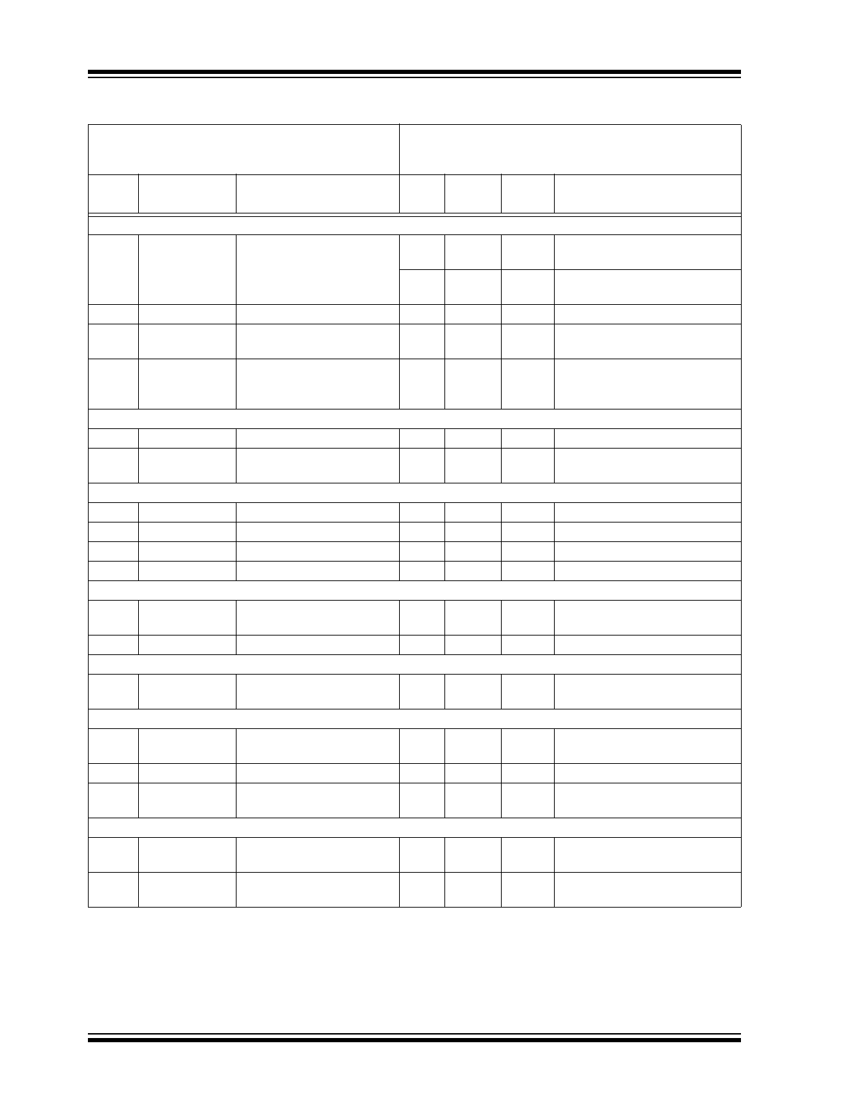
DC Characteristics
DC Specifications
Electrical Characteristics:
Industrial (I):
T
AMB
= -40°C to +85°C V
DD
= 4.5V to 5.5V
Extended (E): T
AMB
= -40°C to +125°C V
DD
= 4.5V to 5.5V
Param
No.
Sym
Characteristic
Min
Max
Units
Conditions
Supply
D1
I
DD
Supply Current
—
75
mA
Dominant; V
TXD
= 0.8V; V
DD
D2
—
10
mA
Recessive; V
TXD
= +2V;
R
S
= 47 kW
D3
—
365
µA
-40°C
T
AMB
+85°C, Standby;
(
Note 2
)
—
465
µA
-40°C
T
AMB
+125°C,
Standby; (
Note 2
)
D4
V
PORH
High-level of the Power-on
Reset comparator
3.8
4.3
V
CANH, CANL outputs are active
when V
DD
> V
PORH
D5
V
PORL
Low-level of the Power-on
Reset comparator
3.4
4.0
V
CANH, CANL outputs are not
active when V
DD
< V
PORL
D6
V
PORD
Hysteresis of Power-on
Reset comparator
0.3
0.8
V
Note 1
Bus Line (CANH; CANL) Transmitter
D7
V
CANH(r);
V
CANL(r)
CANH, CANL Recessive
bus voltage
2.0
3.0
V
V
TXD
= V
DD
; no load.
D8
I
O
(
CANH
)(reces)
I
O
(
CANL
)(reces)
Recessive output current
-2
+2
mA
-2V < V(
CAHL
,
CANH
) < +7V,
0V <V
DD
< 5.5V
D9
-10
+10
mA
-5V < V(
CANL
,
CANH
) < +40V,
0V <V
DD
< 5.5V
D10
V
O
(
CANH
)
CANH Dominant
output voltage
2.75
4.5
V
V
TXD
= 0.8V
D11
V
O
(
CANL
)
CANL Dominant
output voltage
0.5
2.25
V
V
TXD
= 0.8V
D12
V
DIFF
(r)(o)
Recessive differential
output voltage
-500
+50
mV
V
TXD
= 2V; no load
D13
V
DIFF
(d)(o)
Dominant differential
output voltage
1.5
3.0
V
V
TXD
= 0.8V; V
DD
= 5V
40W < R
L
< 60W (
Note 2
)
D14
I
O
(SC)(
CANH
)
CANH short-circuit
output current
—
-200
mA
V
CANH
= -5V
D15
—
-100
(typical)
mA
V
CANH
= -40V, +40V. (
Note 1
)
D16
I
O
(SC)(
CANL
)l
CANL short-circuit
output current
—
200
mA
V
CANL
= -40V, +40V. (
Note 1
)
D17
V
DIFF
(r)(i)
Recessive differential
input voltage
-1.0
+0.5
V
-2V < V(
CANL
,
CANH
) < +7V
(
Note 3
)
-1.0
+0.4
V
-12V < V(
CANL
,
CANH
) < +12V
(
Note 3
)
Note 1:
This parameter is periodically sampled and not 100% tested.
2:
I
TXD
= I
RXD
= I
VREF
= 0 mA; 0V < V
CANL
< V
DD
; 0V < V
CANH
< V
DD
; V
RS
= V
DD.
3:
This is valid for the receiver in all modes; High-speed, Slope-control and Standby.
MCP2551
DS20001667G-page 10
2001-2016 Microchip Technology Inc.
Bus Line (CANH; CANL) Receiver: [TXD = 2V; pins 6 and 7 externally driven]
D18
V
DIFF
(d)(i)
Dominant differential
input voltage
0.9
5.0
V
-2V < V(
CANL
,
CANH
) < +7V
(
Note 3
)
1.0
5.0
V
-12V < V(
CANL
,
CANH
) < +12V
(
Note 3
)
D19
V
DIFF
(h)(i)
Differential input hysteresis
100
200
mV
See
Figure 2-3
(
Note 1
)
D20
R
IN
CANH, CANL Common-
mode input resistance
5
50
kW
D21
R
IN
(d)
Deviation between CANH
and CANL Common-mode
input resistance
-3
+3
%
V
CANH
= V
CANL
Bus Line (CANH; CANL) Receiver: [TXD = 2V; pins 6 and 7 externally driven]
D22
R
DIFF
Differential input resistance
20
100
kW
D24
I
LI
CANH, CANL input leakage
current
—
150
µA
V
DD
< V
POR
;
V
CANH
= V
CANL
= +5V
Transmitter Data Input (TXD)
D25
V
IH
High-level input voltage
2.0
V
DD
V
Output Recessive
D26
V
IL
Low-level input voltage
V
SS
+0.8
V
Output Dominant
D27
I
IH
High-level input current
-1
+1
µA
V
TXD
= V
DD
D28
I
IL
Low-level input current
-100
-400
µA
V
TXD
= 0V
Receiver Data Output (RXD)
D31
V
OH
High-level output voltage
0.7 V
D
D
—
V
I
OH
= 8 mA
D32
V
OL
Low-level output voltage
—
0.8
V
I
OL
= 8 mA
Voltage Reference Output (V
REF
)
D33
V
REF
Reference output voltage
0.45 V
DD
0.55 V
D
D
V
-50 µA < I
VREF
< 50 µA
Standby/Slope-Control (R
S
pin)
D34
V
STB
Input voltage for standby
mode
0.75 V
DD
—
V
D35
I
SLOPE
Slope-control mode current
-10
-200
µA
D36
V
SLOPE
Slope-control mode voltage
0.4 V
D
D
0.6 V
DD
V
Thermal Shutdown
D37
T
J(sd)
Shutdown junction
temperature
155
180
o
C
Note 1
D38
T
J(h)
Shutdown temperature
hysteresis
20
30
o
C
-12V < V(
CANL
,
CANH
) < +12V
(
Note 3
)
2.2
DC Characteristics (Continued)
DC Specifications (Continued)
Electrical Characteristics:
Industrial (I):
T
AMB
= -40°C to +85°C V
DD
= 4.5V to 5.5V
Extended (E): T
AMB
= -40°C to +125°C V
DD
= 4.5V to 5.5V
Param
No.
Sym
Characteristic
Min
Max
Units
Conditions
Note 1:
This parameter is periodically sampled and not 100% tested.
2:
I
TXD
= I
RXD
= I
VREF
= 0 mA; 0V < V
CANL
< V
DD
; 0V < V
CANH
< V
DD
; V
RS
= V
DD.
3:
This is valid for the receiver in all modes; High-speed, Slope-control and Standby.