
2016 Microchip Technology Inc.
DS20005514A-page 1
MCP2542FD/4FD,
MCP2542WFD/4WFD
Features
• Supports CAN 2.0 and CAN with Flexible Data Rate
(CAN FD) Physical Layer Transceiver Requirements
• Optimized for CAN FD at 2, 5 and 8 Mbps Operation
- Maximum propagation delay: 120 ns
- Loop delay symmetry: -10%/+10% (2 Mbps)
• MCP2542FD/4FD:
- Wake-up on CAN activity, 3.6 µs filter time
• MCP2542WFD/4WFD:
- Wake-up on Pattern (WUP), as specified in
ISO11898-2:2015, 3.6 µs activity filter time
• Implements ISO11898-2:2003, ISO11898-5:2007, and
ISO/DIS11898-2:2015
• Qualification: AEC-Q100 Rev. G, Grade 0 (-40°C to
+150°C)
• Very Low Standby Current (4 µA, typical)
• V
IO
Supply Pin to Interface Directly to CAN Controllers
and Microcontrollers with 1.8V to 5V I/O
• CAN Bus Pins are Disconnected when Device is
Unpowered
- An unpowered node or brown-out event will not
load the CAN bus
- Device is unpowered if V
DD
or V
IO
drop below its
POR level
• Detection of Ground Fault:
- Permanent Dominant detection on T
XD
- Permanent Dominant detection on bus
• Automatic Thermal Shutdown Protection
• Suitable for 12V and 24V Systems
• Meets or Exceeds Stringent Automotive Design
Requirements Including “Hardware Requirements for
LIN, CAN and FlexRay Interfaces in Automotive
Applications”, Version 1.3, May 2012
- Conducted emissions @ 2 Mbps with
Common-Mode Choke (CMC)
- Direct Power Injection (DPI) @ 2 Mbps with CMC
• Meets SAE J2962/2 “Communication Transceiver Quali-
fication Requirements - CAN”
- Radiated emissions @ 2 Mbps without a CMC
• High Electrostatic Discharge (ESD) Protection on CANH
and CANL, meeting IEC61000-4-2 up to ±13 kV
• Temperature ranges:
- Extended (E): -40°C to +125°C
- High (H): -40°C to +150°C
Description
The MCP2542FD/4FD and MCP2542WFD/4WFD CAN
transceiver family is designed for high-speed CAN FD
applications up to 8 Mbps communication speed. The
maximum propagation delay was improved to support longer
bus length.
The device meets the automotive requirements for CAN FD bit
rates exceeding 2 Mbps, low quiescent current,
electromagnetic compatibility (EMC) and electrostatic
discharge (ESD).
Applications
CAN 2.0 and CAN FD networks in Automotive, Industrial,
Aerospace, Medical, and Consumer applications.
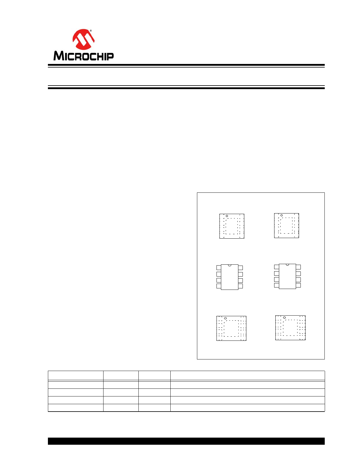
Package Types
MCP2542FD/4FD, MCP2542WFD/4WFD Family Members
MCP2542FD
MCP2542WFD
8-Lead SOIC
V
DD
V
SS
R
XD
CANH
CANL
1
2
3
4
8
7
6
5 V
IO
STBY
T
XD
MCP2544FD
MCP2544WFD
8-Lead SOIC
VDD
VSS
RXD
CANH
CANL
1
2
3
4
8
7
6
5 NC
STBY
TXD
V
DD
V
SS
R
XD
CANH
CANL
1
2
3
4
8
7
6
5 NC
STBY
T
XD
EP
9
V
DD
V
SS
R
XD
CANH
CANL
1
2
3
4
8
7
6
5 V
IO
STBY
T
XD
EP
9
* Includes Exposed Thermal Pad (EP); see
Table 1-1
.
MCP2544FD
MCP2544WFD
3x3 DFN*
MCP2542FD
MCP2542WFD
3x3 DFN*
V
DD
V
SS
R
XD
CANH
CANL
1
2
3
4
8
7
6
5
V
IO
STBY
T
XD
EP
9
V
DD
V
SS
R
XD
CANH
CANL
1
2
3
4
8
7
6
5
NC
STBY
T
XD
EP
9
MCP2542FD
MCP2542WFD
2x3 TDFN*
MCP2544FD
MCP2544WFD
2x3 TDFN*
Device
V
IO
pin
WUP
Description
MCP2542FD
Yes
No
MCP2544FD
No
No
Internal level shifter on digital I/O pins
MCP2542WFD
Yes
Yes
Wake-Up on Pattern (see
Section 1.6.5
)
MCP2544WFD
No
Yes
Internal level shifter on digital I/O pins; Wake-Up on Pattern
Note: For ordering information, see the
Product Identification System
section.
CAN FD Transceiver with Wake-Up Pattern (WUP) Option
MCP2542FD/4FD, MCP2542WFD/4WFD
DS20005514A-page 2
2016 Microchip Technology Inc.
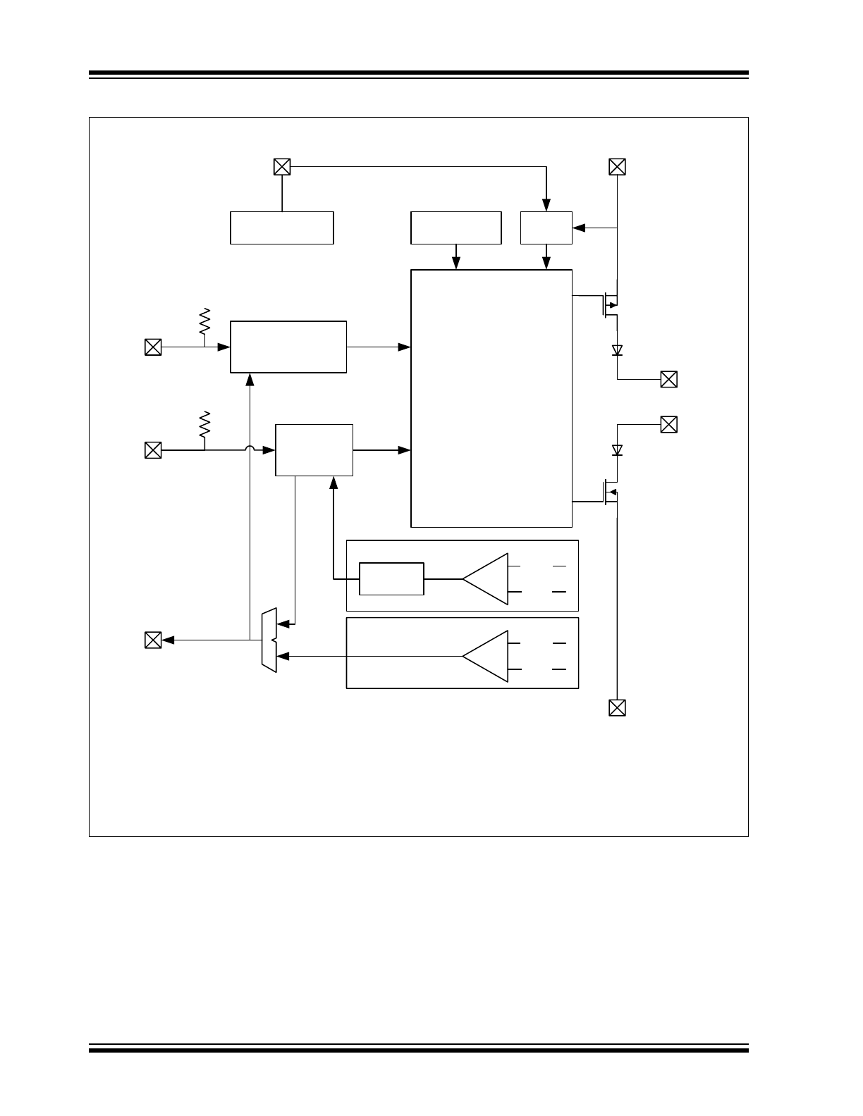
Block Diagram
Note 1: There is one receiver implemented. The receiver can operate in Low-Power or High-Speed mode.
2: Only MCP2542FD and MCP2542WFD have the V
IO
pin.
3: In the MCP2544FD and MCP2544WFD, the supply for the digital I/O is internally connected to V
DD
.
V
DD
CANH
CANL
T
XD
R
XD
Driver
and
Slope Control
Thermal
Protection
POR
UVLO
Digital I/O
Supply
V
IO
V
SS
STBY
Permanent Dominant
Detect
V
IO
V
IO
Mode Control
Wake-Up
Filter
CANH
CANL
CANH
CANL
LP_RX
HS_RX
V
DD
V
DD

2016 Microchip Technology Inc.
DS20005514A-page 3
MCP2542FD/4FD, MCP2542WFD/4WFD
1.0
DEVICE OVERVIEW
The MCP2542FD/4FD and MCP2542WFD/4WFD
devices serve as the interface between a CAN protocol
controller and the physical bus. The devices provide
differential transmit and receive capability for the CAN
protocol controller. The devices are fully compatible
with the ISO11898-2 and ISO11898-5 standards, and
with the ISO/DIS11898-2:2015 working draft.
Excellent Loop Delay Symmetry supports data rates up
to 8 Mbps for CAN FD. The maximum propagation
delay was improved to support longer bus length.
Typically, each node in a CAN system must have a
device to convert the digital signals generated by a
CAN controller to signals suitable for transmission over
the bus cabling (differential output). It also provides a
buffer between the CAN controller and the high-voltage
spikes that can be generated on the CAN bus by
outside sources.
The MCP2542FD/4FD wakes up on CAN activity (basic
wake-up). The CAN activity filter time is 3.6 µs maximum.
The MCP2542WFD/4WFD wakes up after receiving
two consecutive dominant states separated by a reces-
sive state: WUP. The minimum duration of each domi-
nant and recessive state is t
FILTER
. The complete WUP
has to be detected within t
WAKE
(
TO
).
1.1
Transmitter Function
The CAN bus has two states: Dominant and
Recessive. A Dominant state occurs when the
differential voltage between CANH and CANL is
greater than V
DIFF
(
D
)(
I
). A Recessive state occurs
when the differential voltage is less than V
DIFF
(
R
)(
I
).
The Dominant and Recessive states correspond to the
Low and High states of the T
XD
input pin, respectively.
However, a Dominant state initiated by another CAN
node will override a Recessive state on the CAN bus.
1.2
Receiver Function
In Normal mode, the R
XD
output pin reflects the
differential bus voltage between CANH and CANL. The
Low and High states of the R
XD
output pin correspond
to the Dominant and Recessive states of the CAN bus,
respectively.
1.3
Internal Protection
CANH and CANL are protected against battery short
circuits and electrical transients that can occur on the
CAN bus. This feature prevents destruction of the
transmitter output stage during such a fault condition.
The device is further protected from excessive current
loading by thermal shutdown circuitry that disables the
output drivers when the junction temperature exceeds
a nominal limit of +175°C.
All other parts of the chip remain operational, and the
chip temperature is lowered due to the decreased
power dissipation in the transmitter outputs. This
protection is essential to protect against bus line
short-circuit-induced damage. Thermal protection is
only active during Normal mode.
1.4
Permanent Dominant Detection
The MCP2542FD/4FD and MCP2542WFD/4WFD
device prevents two conditions:
• Permanent Dominant condition on T
XD
• Permanent Dominant condition on the bus
In Normal mode, if the MCP2542FD/4FD and
MCP2542WFD/4WFD detects an extended Low state
on the T
XD
input, it will disable the CANH and CANL
output drivers in order to prevent the corruption of data
on the CAN bus. The drivers will remain disabled until
T
XD
goes High. The high-speed receiver is active and
data on the CAN bus is received on R
XD
.
In Standby mode, if the MCP2542FD/4FD and
MCP2542WFD/4WFD detects an extended dominant
condition on the bus, it will set the R
XD
pin to a
Recessive state. This allows the attached controller to
go to Low-Power mode until the dominant issue is
corrected. R
XD
is latched High until a Recessive state
is detected on the bus and the Wake-Up function is
enabled again.
1.5
Power-On Reset (POR) and
Undervoltage Detection
The MCP2542FD/4FD and MCP2542WFD/4WFD
have POR detection on both supply pins: V
DD
and V
IO
.
Typical POR thresholds to deassert the reset are 1.2V
and 3.0V for V
IO
and V
DD
, respectively.
When the device is powered on, CANH and CANL
remain in a high-impedance state until V
DD
exceeds its
undervoltage level. Once powered on, CANH and
CANL will enter a high-impedance state if the voltage
level at V
DD
drops below the undervoltage level,
providing voltage brown-out protection during normal
operation.
In Normal mode, the receiver output is forced to
Recessive state during an undervoltage condition on
V
DD
. In Standby mode, the low-power receiver is
designed to work down to 1.7V V
IO
. Therefore, the
low-power receiver remains operational down to V
PORL
on V
DD
(MCP2544FD and MCP2544WFD). The
MCP2542FD and MCP2542WFD transfers data to the
R
XD
pin down to 1.7V on the V
IO
supply.

MCP2542FD/4FD, MCP2542WFD/4WFD
DS20005514A-page 4
2016 Microchip Technology Inc.
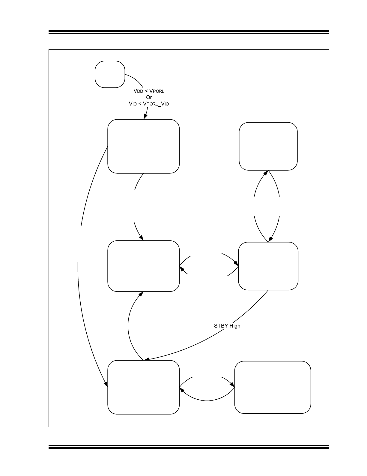
1.6
Mode Control
The main difference between the MCP2542FD/4FD
and MCP2542WFD/4WFD is the wake-up method.
Figure 1-1
shows the state diagram of the
MCP2542FD/4FD. The devices wake up on CAN activity.
Figure 1-2
shows the state diagram of the
MCP2542WFD/4WFD. The devices wake up on a
WUP.
1.6.1
UNPOWERED MODE (POR)
The MCP2542FD/4FD and MCP2542WFD/4WFD
enter Unpowered mode under the following conditions:
• After powering up the device, or
• If V
DD
drops below V
PORL
, or
• If V
IO
drops below V
PORL
_V
IO
.
In Unpowered mode, the CAN bus will be biased to
ground using a high impedance. The
MCP2542FD/4FD and MCP2542WFD/4WFD are not
able to communicate on the bus or detect a wake-up
event.
1.6.2
WAKE MODE
The MCP2542FD/4FD and MCP2542WFD/4WFD
transitions from Unpowered mode to Wake mode
when V
DD
and V
IO
are above their PORH levels. From
Normal mode, the device will also enter Wake mode if
V
DD
is smaller than V
UVL
, or if the band gap output
voltage is not within valid range. Additionally, the
device will transition from Standby mode to Wake
mode if STBY is pulled Low.
In Wake mode, the CAN bus is biased to ground and
R
XD
is always high.
1.6.3
NORMAL MODE
When V
DD
exceeds V
UVH
, the band gap is within valid
range and T
XD
is High, the device transitions into
Normal mode. During POR, when the microcontroller
powers up, the T
XD
pin could be unintentionally pulled
down by the microcontroller powering up. To avoid
driving the bus during a POR of the microcontroller,
the transceiver proceeds to Normal mode only after
T
XD
is high.
In Normal mode, the driver block is operational and
can drive the bus pins. The slopes of the output
signals on CANH and CANL are optimized to reduce
Electromagnetic Emissions (EME). The CAN bus is
biased to V
DD
/2.
The high-speed differential receiver is active.
1.6.4
STANDBY MODE
The device may be placed in Standby mode by
applying a high level to the STBY pin. In Standby
mode, the transmitter and the high-speed part of the
receiver are switched off to minimize power
consumption.
The low-power receiver and the wake-up block are
enabled in order to monitor the bus for activity. The
CAN bus is biased to ground.
The R
XD
pin remains HIGH until a wake-up event has
occurred.
The MCP2542FD/4FD uses Basic Wake-Up: one
dominant phase for a minimum time of t
FILTER
will
wake up the device.
The MCP2542WFD/4WFD will only wake up if it
detects a complete WUP. The WUP method is
described in the next section.
After a wake-up event was detected, the CAN
controller gets interrupted by a negative edge on the
R
XD
pin.
The CAN controller must put the MCP2542FD/4FD and
MCP2542WFD/4WFD back into Normal mode by
deasserting the STBY pin in order to enable
high-speed data communication.
The CAN bus Wake-Up function requires both supply
voltages, V
DD
and V
IO
, to be in valid range.
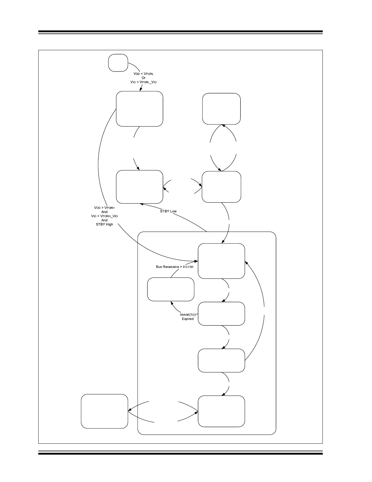
1.6.5
REMOTE WAKE-UP VIA CAN BUS (WUP)
The MCP2542WFD/4WFD wakes up from
Standby/Silent mode when a dedicated wake-up pat-
tern (WUP) is detected on the CAN bus. The wake-up
pattern is specified in ISO11898-6 and
ISO/DIS11898-2:2015 (see
Figure 1-2
and
Figure 2-11
).
The Wake-Up Pattern consists of three events:
• a Dominant phase of at least t
FILTER
, followed by
• a Recessive phase of at least t
FILTER
, followed by
• a Dominant phase of at least t
FILTER
The complete pattern must be received within
t
WAKE
(
TO
). Otherwise, the internal wake-up logic is
reset and the complete wake-up pattern must be
retransmitted in order to trigger a wake-up event.
2016 Microchip Technology Inc.
DS20005514A-page 5
MCP2542FD/4FD, MCP2542WFD/4WFD
FIGURE 1-1:
MCP2542FD/4FD STATE DIAGRAM: BASIC WAKE-UP
V
DD
> V
PORH
And
V
IO
> V
PORH
_V
IO
And
STBY High
Bandgap not OK
Or
V
DD
< V
UVL
T
XD
High
And
Bandgap OK
And
V
DD
> V
UVH
Bus Recessive
Bus Dominant > t
PDT
STBY Low
T
XD
High
And
T < TJ(SD)-TJ(HYST)
T
XD
Low > T
PDT
Or
T > TJ(SD)
V
DD
> V
PORH
And
V
IO
> V
PORH
_V
IO
And
STBY Low
Normal
CAN Driven
Common mode V
DD
/2
HS RX ON
Wake-Up Disabled
R
XD
= f(HS RX)
T
XD
Time Out
CAN Recessive
Common mode V
DD
/2
HS RX ON
Wake-Up Disabled
5
;'
I+65;
Un
Sowered (POR)
CAN High Impedance
Common mode tied to GND
HS RX OFF
Wake-Up Disabled
R
XD
High
Bandgap OFF
From any
Vtate
Standby
CAN High Impedance
Common mode tied to GND
HS RX OFF
Wake-Up Enabled
R
XD
= f(LP RX)
Stop Bandgap
Bus Dominant
Time Out
CAN High Impedance
Common mode tied to GND
HS RX OFF
Wake-Up Disabled
R
XD
High
Wake
Start Bandgap
CAN High Impedance
Common mode tied to GND
HS RX OFF
Wake-Up Disabled
R
XD
High
MCP2542FD/4FD, MCP2542WFD/4WFD
DS20005514A-page 6
2016 Microchip Technology Inc.
FIGURE 1-2:
MCP2542WFD/4WFD STATE DIAGRAM: WAKE-UP PATTERN
t
WAKE
(
TO
)
Expired
Bus Recessive
Bus Dominant > t
FILTER
Bus Recessive > t
FILTER
Bus Dominant > t
FILTER
Bandgap Not Ok
Or
V
DD
< V
UVL
T
XD
High
And
Bandgap OK
And
V
DD
> V
UVH
Bus Dominant > t
PDT
STBY High
T
XD
High
And
T < TJ(SD)-TJ(HYST)
T
XD
Low > T
PDT
Or
T > TJ(SD)
V
DD
> V
PORH
And
V
IO
> V
PORH
_V
IO
And
STBY Low
Normal
CAN Driven
Common mode V
DD
/2
HS RX ON
Wake-Up Disabled
R
XD
= f(HS RX)
TXD Time Out
CAN Recessive
Common mode V
DD
/2
HS RX ON
Wake-Up Disabled
R
XD
= f(HS RX)
UnPowered (POR)
CAN High Impedance
Common mode tied to GND
HS RX OFF
Wake-Up Disabled
R
XD
High
Bandgap OFF
From any
State
Standby Init
CAN High Impedance
Common mode tied to GND
HS RX OFF
Wake-Up Enabled
R
XD
High
Stop Bandgap
Wake
Start Bandgap
CAN High Impedance
Common mode tied to GND
HS RX OFF
Wake-Up Disabled
R
XD
High
Standby 1
Start t
WAKE
TIME
OUT
R
XD
High
Standby 2
R
XD
High
Standby/Receiving
CAN High Impedance
Common mode tied to GND
HS RX OFF
R
XD
= f(LP RX)
Standby
Bus Dominant
Time Out
CAN High Impedance
Common mode tied to GND
HS RX OFF
Wake-Up Disabled
R
XD
High
Standby 3
R
XD
High
2016 Microchip Technology Inc.
DS20005514A-page 7
MCP2542FD/4FD, MCP2542WFD/4WFD
1.7
Pin Descriptions
The description of the pins are listed in
Table 1-1
.
1.7.1
TRANSMITTER DATA
INPUT PIN (T
XD
)
The CAN transceiver drives the differential output pins
CANH and CANL according to T
XD
. It is usually
connected to the transmitter data output of the CAN
controller device. When T
XD
is Low, CANH and CANL
are in the Dominant state. When T
XD
is High, CANH
and CANL are in the Recessive state, provided that
another CAN node is not driving the CAN bus with a
Dominant state. T
XD
is connected from an internal
pull-up resistor (nominal 33 k
) to V
IO
in the
MCP2542FD and MCP2542WFD, and to V
DD
in the
MCP2544FD and MCP2544WFD.
1.7.2
GROUND SUPPLY PIN (V
SS
)
Ground supply pin.
1.7.3
SUPPLY VOLTAGE PIN (V
DD
)
Positive supply voltage pin. Supplies transmitter and
receiver, including the wake-up receiver.
1.7.4
RECEIVER DATA OUTPUT PIN (R
XD
)
R
XD
is a CMOS-compatible output that drives High or
Low depending on the differential signals on the CANH
and CANL pins, and is usually connected to the
receiver data input of the CAN controller device. R
XD
is
High when the CAN bus is Recessive, and Low in the
Dominant state. R
XD
is supplied by V
IO
in the
MCP2542FD and MCP2542WFD and by V
DD
in the
MCP2544FD and MCP2544WFD.
1.7.5
NC PIN (MCP2544FD AND
MCP2544WFD)
No Connect. This pin can be left open or connected to
V
SS
.
1.7.6
V
IO
PIN (MCP2542FD AND
MCP2542WFD)
Supply for digital I/O pins. In the MCP2544FD and
MCP2544WFD, the supply for the digital I/O (T
XD
, R
XD
and STBY) is internally connected to V
DD
.
1.7.7
DIGITAL I/O
The MCP2542FD/4FD and MCP2542WFD/4WFD
enable easy interfacing to MCU with I/O ranges from
1.8V to 5V.
1.7.7.1
MCP2544FD and MCP2544WFD
The V
IH
(
MIN
) and V
IL
(
MAX
) for STBY and T
XD
are
independent of V
DD
. They are set at levels that are
compatible with 3V and 5V microcontrollers.
The R
XD
pin is always driven to V
DD
, therefore a 3V
microcontroller will need a 5V tolerant input.
1.7.7.2
MCP2542FD and MCP2542WFD
V
IH
and V
IL
for STBY and T
XD
depend on V
IO
. The
R
XD
pin is driven to V
IO
.
1.7.8
CAN LOW PIN (CANL)
The CANL output drives the Low side of the CAN
differential bus. This pin is also tied internally to the
receive input comparator. CANL disconnects from the
bus when MCP2542FD/4FD and
MCP2542WFD/4WFD are not powered.
1.7.9
CAN HIGH PIN (CANH)
The CANH output drives the high side of the CAN
differential bus. This pin is also tied internally to the
receive input comparator. CANH disconnects from the
bus when MCP2542FD/4FD and
MCP2542WFD/4WFD are not powered.
TABLE 1-1:
MCP2542/4FD AND MCP2542/4WFD PIN DESCRIPTIONS
MCP2542FD
MCP2542WFD
3x3 DFN,
2x3TDFN
MCP2542FD
MCP2542WFD
SOIC
MCP2544FD
MCP2544WFD
3x3 DFN,
2x3TDFN
MCP2544FD
MCP2544WFD
SOIC
Symbol
Pin Function
1
1
1
1
T
XD
Transmit Data Input
2
2
2
2
V
SS
Ground
3
3
3
3
V
DD
Supply Voltage
4
4
4
4
R
XD
Receive Data Output
—
—
5
5
NC
No Connect
5
5
—
—
V
IO
Digital I/O Supply Pin
6
6
6
6
CANL
CAN Low-Level Voltage I/O
7
7
7
7
CANH
CAN High-Level Voltage I/O
8
8
8
8
STBY
Standby Mode Input
9
—
9
—
EP
Exposed Thermal Pad

MCP2542FD/4FD, MCP2542WFD/4WFD
DS20005514A-page 8
2016 Microchip Technology Inc.
1.7.10
STANDBY MODE INPUT PIN (STBY)
This pin selects between Normal or Standby mode. In
Standby mode, the transmitter and high-speed receiver
are turned off, only the low-power receiver and wake-up
filter are active. STBY is connected from an internal
MOS pull-up resistor to V
IO
in the MCP2542FD and
MCP2542WFD, and to V
DD
in the MCP2544FD and
MCP2544WFD. The value of the MOS pull-up resistor
depends on the supply voltage. Typical values are
660 k
for 5V, 1.1 M for 3.3V and 4.4 M for 1.8V.
1.7.11
EXPOSED THERMAL PAD (EP)
It is recommended to connect this pad to V
SS
to
enhance electromagnetic immunity and thermal
resistance.
2016 Microchip Technology Inc.
DS20005514A-page 9
MCP2542FD/4FD, MCP2542WFD/4WFD
1.8
Typical Applications
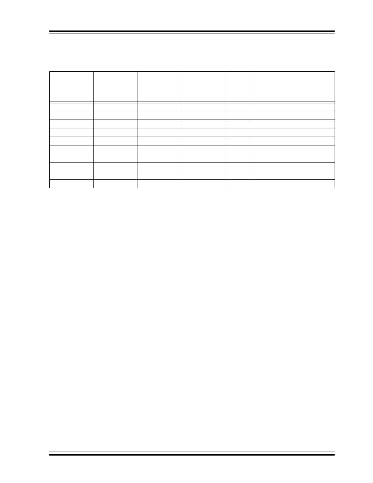
In order to meet the EMC/EMI requirements, a
Common Mode Choke (CMC) may be required for data
rates greater than 1 Mbps.
Figure 1-3
and
Figure 1-4
illustrate examples of typical applications of the
devices.
FIGURE 1-3:
MCP2544WFD WITH NC AND SPLIT TERMINATION
FIGURE 1-4:
MCP2542FD WITH V
IO
PIN
5V LDO
V
BAT
V
DD
V
DD
T
XD
R
XD
STBY
CANTX
CANRX
RBX
V
SS
V
SS
PI
C
®
MC
U
MC
P
2
544
W
F
D
NC
CANH
CANL
0.1 µF
CANH
CANL
4700 pF
60
60
3.3V LDO
V
DD
V
DD
TXD
RXD
STBY
CANTX
CANRX
RBX
V
SS
V
SS
PI
C
®
MC
U
MC
P
2542
F
D
CANH
CANL
5V LDO
V
BAT
V
IO
0.1 µF
0.1 µF
CANH
CANL
120
EN
RBX

MCP2542FD/4FD, MCP2542WFD/4WFD
DS20005514A-page 10
2016 Microchip Technology Inc.
NOTES: