
2003-2016 Microchip Technology Inc.
DS20001801H-page 1
MCP2515
Features
• Implements CAN V2.0B at 1 Mb/s:
- 0 to 8-byte length in the data field
- Standard and extended data and remote
frames
• Receive Buffers, Masks and Filters:
- Two receive buffers with prioritized message
storage
- Six 29-bit filters
- Two 29-bit masks
• Data Byte Filtering on the First Two Data Bytes
(applies to standard data frames)
• Three Transmit Buffers with Prioritization and
Abort Features
• High-Speed SPI Interface (10 MHz):
- SPI modes 0,0 and 1,1
• One-Shot mode Ensures Message Transmission
is Attempted Only One Time
• Clock Out Pin with Programmable Prescaler:
- Can be used as a clock source for other
device(s)
• Start-of-Frame (SOF) Signal is Available for
Monitoring the SOF Signal:
- Can be used for time slot-based protocols
and/or bus diagnostics to detect early bus
degradation
• Interrupt Output Pin with Selectable Enables
• Buffer Full Output Pins Configurable as:
- Interrupt output for each receive buffer
- General purpose output
• Request-to-Send (RTS) Input Pins Individually
Configurable as:
- Control pins to request transmission for each
transmit buffer
- General purpose inputs
• Low-Power CMOS Technology:
- Operates from 2.7V-5.5V
- 5 mA active current (typical)
- 1 µA standby current (typical) (Sleep mode)
• Temperature Ranges Supported:
- Industrial (I): -40°C to +85°C
- Extended (E): -40°C to +125°C
Description
Microchip Technology’s MCP2515 is a stand-alone
Controller Area Network (CAN) controller that imple-
ments the CAN specification, Version 2.0B. It is capable
of transmitting and receiving both standard and
extended data and remote frames. The MCP2515 has
two acceptance masks and six acceptance filters that
are used to filter out unwanted messages, thereby
reducing the host MCU’s overhead. The MCP2515
interfaces with microcontrollers (MCUs) via an industry
standard Serial Peripheral Interface (SPI).
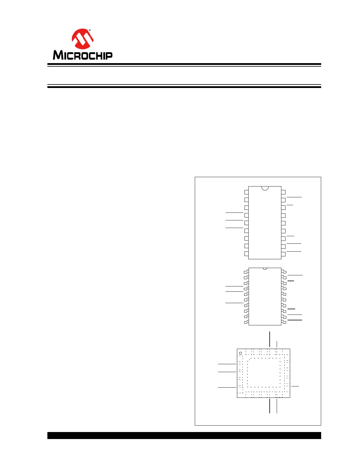
Package Types
16
5
TXCAN
RXCAN
V
DD
RESET
CS
SO
M
C
P251
5
1
2
3
4
18
17
16
15
SI
SCK
INT
RX0BF
14
13
12
11
RX1BF
10
OSC2
OSC1
CLKOUT/SOF
TX2RTS
5
6
7
8
V
SS
9
TX0RTS
TX1RTS
TXCAN
RXCAN
TX0RTS
OSC1
CLKOUT/SOF
OSC2
CS
V
DD
RESET
SO
SCK
INT
SI
RX0BF
RX1BF
V
SS
TX1RTS
TX2RTS
NC
NC
18-Lead PDIP/SOIC
20-Lead TSSOP
2
NC
TX2RTS
TX0RTS
SO
SI
OS
C2
NC
OS
C1
GND
RX
1B
F
SCK
RX
C
A
N
TXC
A
N
V
DD
RE
S
E
T
TX1RTS
EP
20
1
19 18 17
3
4
14
13
12
11
6
7
8
9
21
10
15
CLKOUT
CS
INT
RX
0
B
F
* Includes Exposed Thermal Pad (EP); see
Table 1-1
.
13
12
1
2
3
4
5
6
7
8
9
20
19
18
17
16
15
14
11
10
MCP
2
51
5
20-Lead QFN*
Stand-Alone CAN Controller with SPI Interface

MCP2515
DS20001801H-page 2
2003-2016 Microchip Technology Inc.
NOTES:
2003-2016 Microchip Technology Inc.
DS20001801H-page 3
MCP2515
1.0
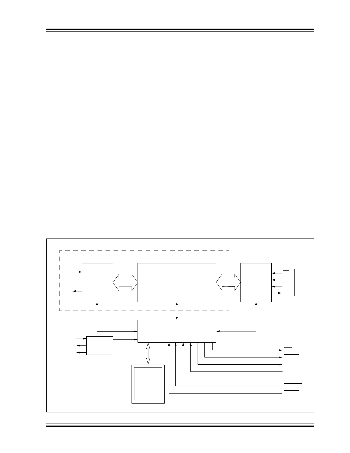
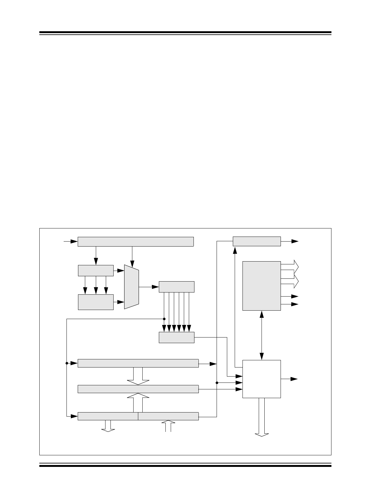
DEVICE OVERVIEW
The MCP2515 is a stand-alone CAN controller devel-
oped to simplify applications that require interfacing
with a CAN bus. A simple block diagram of the
MCP2515 is shown in
Figure 1-1
. The device consists
of three main blocks:
1.
The CAN module, which includes the CAN
protocol engine, masks, filters, transmit and
receive buffers.
2.
The control logic and registers that are used to
configure the device and its operation.
3.
The SPI protocol block.
An example system implementation using the device is
shown in
Figure 1-2
.
1.1
CAN Module
The CAN module handles all functions for receiving and
transmitting messages on the CAN bus. Messages are
transmitted by first loading the appropriate message buf-
fer and control registers. Transmission is initiated by
using control register bits via the SPI interface or by
using the transmit enable pins. Status and errors can be
checked by reading the appropriate registers. Any
message detected on the CAN bus is checked for errors
and then matched against the user-defined filters to see
if it should be moved into one of the two receive buffers.
1.2
Control Logic
The control logic block controls the setup and operation
of the MCP2515 by interfacing to the other blocks in
order to pass information and control.
Interrupt pins are provided to allow greater system
flexibility. There is one multipurpose interrupt pin (as
well as specific interrupt pins) for each of the receive
registers that can be used to indicate a valid message
has been received and loaded into one of the receive
buffers. Use of the specific interrupt pins is optional.
The general purpose interrupt pin, as well as status
registers (accessed via the SPI interface), can also be
used to determine when a valid message has been
received.
Additionally, there are three pins available to initiate
immediate transmission of a message that has been
loaded into one of the three transmit registers. Use of
these pins is optional, as initiating message transmis-
sions can also be accomplished by utilizing control
registers accessed via the SPI interface.
1.3
SPI Protocol Block
The MCU interfaces to the device via the SPI interface.
Writing to, and reading from, all registers is
accomplished using standard SPI read and write
commands, in addition to specialized SPI commands.
FIGURE 1-1:
BLOCK DIAGRAM
SPI
Interface
Logic
SPI
Bus
INT
CS
SCK
SI
SO
CAN
Protocol
Engine
RXCAN
TXCAN
Control Logic
RX0BF
RX1BF
TX0RTS
TX1RTS
TX2RTS
TX and RX Buffers
Masks and Filters
CAN Module
RESET
Timing
Generation
OSC1
OSC2
CLKOUT
Control
and
Interrupt
Registers
MCP2515
DS20001801H-page 4
2003-2016 Microchip Technology Inc.
FIGURE 1-2:
EXAMPLE SYSTEM IMPLEMENTATION
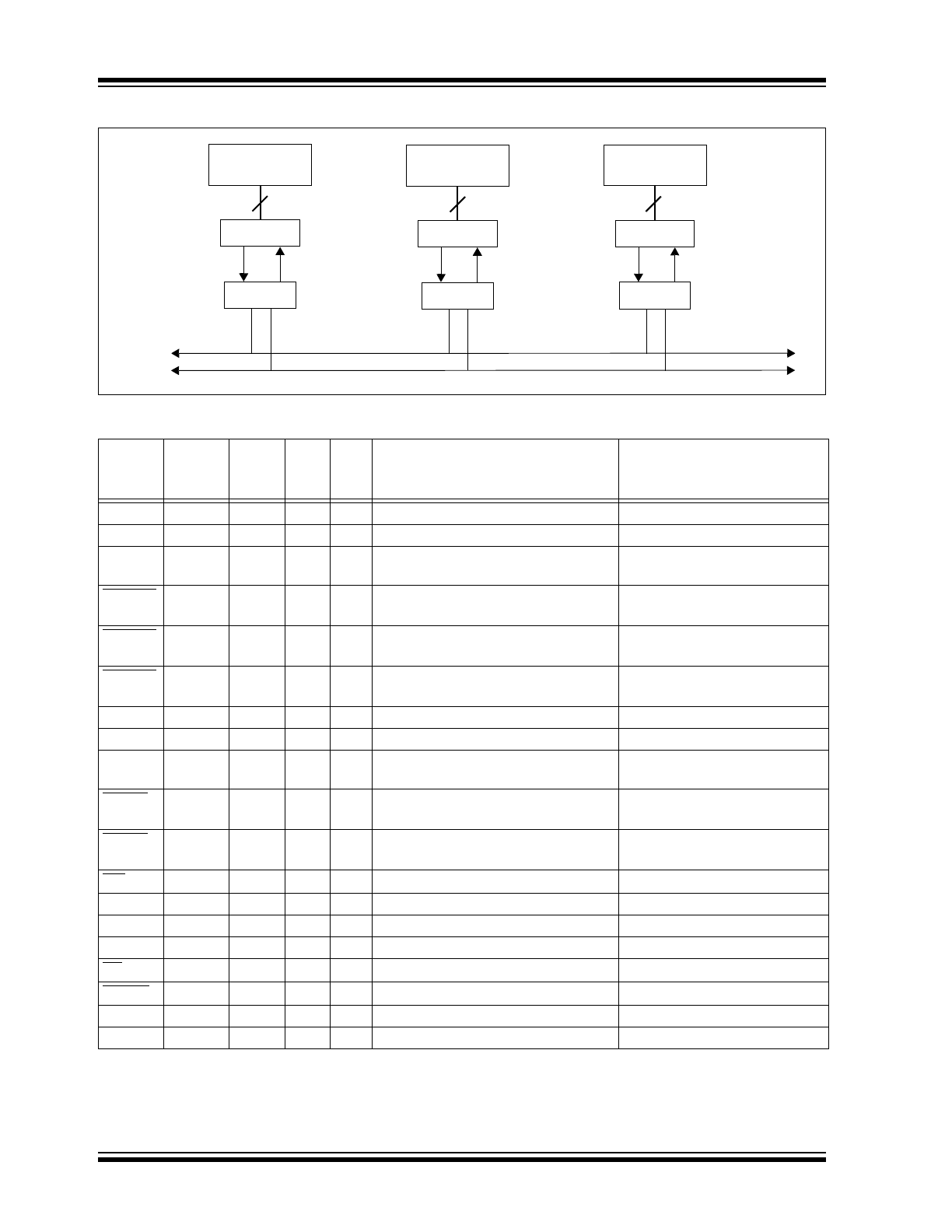
TABLE 1-1:
PINOUT DESCRIPTION
Name
PDIP/
SOIC
Pin #
TSSOP
Pin #
QFN
Pin #
I/O/P
Type
Description
Alternate Pin Function
TXCAN
1
1
19
O
Transmit output pin to CAN bus
—
RXCAN
2
2
20
I
Receive input pin from CAN bus
—
CLKOUT
3
3
1
O
Clock output pin with programmable
prescaler
Start-of-Frame signal
TX0RTS
4
4
2
I
Transmit buffer TXB0 Request-to-Send;
100 k
internal pull-up to V
DD
General purpose digital input,
100 k
internal pull-up to V
DD
TX1RTS
5
5
3
I
Transmit buffer TXB1 Request-to-Send;
100 k
internal pull-up to V
DD
General purpose digital input,
100 k
internal pull-up to V
DD
TX2RTS
6
7
5
I
Transmit buffer TXB2 Request-to-Send;
100 k
internal pull-up to V
DD
General purpose digital input,
100 k
internal pull-up to V
DD
OSC2
7
8
6
O
Oscillator output
—
OSC1
8
9
7
I
Oscillator input
External clock input
V
SS
9
10
8
P
Ground reference for logic and I/O
pins
—
RX1BF
10
11
9
O
Receive buffer RXB1 interrupt pin or
general purpose digital output
General purpose digital output
RX0BF
11
12
10
O
Receive buffer RXB0 interrupt pin or
general purpose digital output
General purpose digital output
INT
12
13
11
O
Interrupt output pin
—
SCK
13
14
12
I
Clock input pin for SPI interface
—
SI
14
16
14
I
Data input pin for SPI interface
—
SO
15
17
15
O
Data output pin for SPI interface
—
CS
16
18
16
I
Chip select input pin for SPI interface
—
RESET
17
19
17
I
Active-low device Reset input
—
V
DD
18
20
18
P
Positive supply for logic and I/O pins
—
NC
—
6,15
4,13
—
No internal connection
—
Legend: I = Input; O = Output; P = Power
XCVR
SPI
TX
RX
CANH
CANL
XCVR
SPI
TX
RX
XCVR
SPI
TX
RX
Node
Controller
MCP2515
Node
Controller
MCP2515
Node
Controller
MCP2515
2003-2016 Microchip Technology Inc.
DS20001801H-page 5
MCP2515
1.4
Transmit/Receive Buffers/Masks/
Filters
The MCP2515 has three transmit and two receive
buffers, two acceptance masks (one for each receive
buffer) and a total of six acceptance filters.
Figure 1-3
shows a block diagram of these buffers and their
connection to the protocol engine.
FIGURE 1-3:
CAN BUFFERS AND PROTOCOL ENGINE BLOCK DIAGRAM
Acceptance Filter
RXF2
R
X
B
1
Identifier
Data Field
Data Field
Identifier
Acceptance Mask
RXM1
Acceptance Filter
RXF3
Acceptance Filter
RXF4
Acceptance Filter
RXF5
M
A
B
Acceptance Filter
RXF0
Acceptance Filter
RXF1
R
X
B
0
TXR
E
Q
TXB2
AB
TF
ML
O
A
TXE
R
R
ME
SS
AGE
Message
Queue
Control
TXR
E
Q
TXB0
AB
TF
ML
O
A
TXE
R
R
ME
SS
AGE
Comparator
Receive
Error
Transmit
Error
Protocol
REC
TEC
ErrPas
BusOff
Finite
State
Machine
Counter
Counter
Shift<14:0>
{Transmit<5:0>, Receive<8:0>}
Transmit
Logic
TX
RX
Configuration
Registers
Clock
Generator
PROTOCOL
ENGINE
BUFFERS
TXR
E
Q
TXB1
AB
TF
ML
O
A
TXE
R
R
ME
SS
AGE
Acceptance Mask
RXM0
A
c
c
e
p
t
A
c
c
e
p
t
SOF
Bit
Timing
Logic
Receive<7:0>
Transmit<7:0>
Transmit Byte Sequencer
CRC<14:0>
MCP2515
DS20001801H-page 6
2003-2016 Microchip Technology Inc.
1.5
CAN Protocol Engine
The CAN protocol engine combines several functional
blocks, shown in
Figure 1-4
and described below.
1.5.1
PROTOCOL FINITE STATE MACHINE
The heart of the engine is the Finite State Machine
(FSM). The FSM is a sequencer that controls the
sequential data stream between the TX/RX Shift
register, the CRC register and the bus line. The FSM
also controls the Error Management Logic (EML) and
the parallel data stream between the TX/RX Shift
registers and the buffers. The FSM ensures that the
processes of reception, arbitration, transmission and
error signaling are performed according to the CAN
protocol. The automatic retransmission of messages
on the bus line is also handled by the FSM.
1.5.2
CYCLIC REDUNDANCY CHECK
The Cyclic Redundancy Check register generates the
Cyclic Redundancy Check (CRC) code, which is
transmitted after either the Control Field (for messages
with 0 data bytes) or the Data Field and is used to
check the CRC field of incoming messages.
1.5.3
ERROR MANAGEMENT LOGIC
The Error Management Logic (EML) is responsible for
the Fault confinement of the CAN device. Its two count-
ers, the Receive Error Counter (REC) and the Transmit
Error Counter (TEC), are incremented and decremented
by commands from the bit stream processor. Based on
the values of the error counters, the CAN controller is set
into the states: error-active, error-passive or bus-off.
1.5.4
BIT TIMING LOGIC
The Bit Timing Logic (BTL) monitors the bus line input
and handles the bus related bit timing according to the
CAN protocol. The BTL synchronizes on a recessive-
to-dominant bus transition at the Start-of-Frame (hard
synchronization) and on any further recessive-to-
dominant bus line transition if the CAN controller itself
does not transmit a dominant bit (resynchronization).
The BTL also provides programmable Time Segments
to compensate for the propagation delay time, phase
shifts and to define the position of the sample point
within the bit time. The programming of the BTL
depends on the baud rate and external physical delay
times.
FIGURE 1-4:
CAN PROTOCOL ENGINE BLOCK DIAGRAM
Bit Timing Logic
CRC<14:0>
Comparator
Receive<7:0>
Transmit<7:0>
Sample<2:0>
Majority
Decision
StuffReg<5:0>
Comparator
Transmit Logic
Receive
Error Counter
Transmit
Error Counter
Protocol
FSM
RX
SAM
BusMon
Rec/Trm Addr.
RecData<7:0>
TrmData<7:0>
Shift<14:0>
(Transmit<5:0>, Receive<7:0>)
TX
REC
TEC
ErrPas
BusOff
Interface to Standard Buffer
SOF

2003-2016 Microchip Technology Inc.
DS20001801H-page 7
MCP2515
2.0
CAN MESSAGE FRAMES
The MCP2515 supports standard data frames, extended
data frames and remote frames (standard and
extended), as defined in the CAN 2.0B specification.
2.1
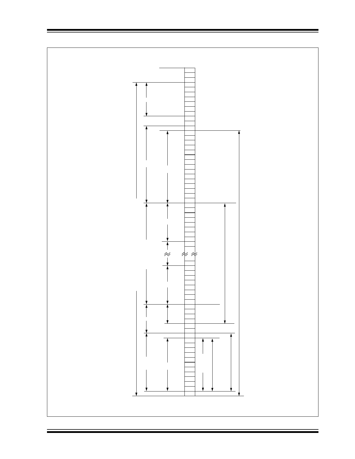
Standard Data Frame
The CAN standard data frame is shown in
Figure 2-1
.
As with all other frames, the frame begins with a Start-
of-Frame (SOF) bit, which is of the dominant state and
allows hard synchronization of all nodes.
The SOF is followed by the arbitration field, consisting
of 12 bits: the 11-bit identifier and the Remote
Transmission Request (RTR) bit. The RTR bit is used
to distinguish a data frame (RTR bit dominant) from a
remote frame (RTR bit recessive).
Following the arbitration field is the control field,
consisting of six bits. The first bit of this field is the
Identifier Extension (IDE) bit, which must be dominant
to specify a standard frame. The following bit, Reserved
Bit Zero (RB0), is reserved and is defined as a dominant
bit by the CAN protocol. The remaining four bits of the
control field are the Data Length Code (DLC), which
specifies the number of bytes of data (0-8 bytes)
contained in the message.
After the control field, is the data field, which contains
any data bytes that are being sent, and is of the length
defined by the DLC (0-8 bytes).
The Cyclic Redundancy Check (CRC) field follows the
data field and is used to detect transmission errors. The
CRC field consists of a 15-bit CRC sequence, followed
by the recessive CRC Delimiter bit.
The final field is the two-bit Acknowledge (ACK) field.
During the ACK Slot bit, the transmitting node sends
out a recessive bit. Any node that has received an
error-free frame Acknowledges the correct reception of
the frame by sending back a dominant bit (regardless
of whether the node is configured to accept that
specific message or not). The recessive Acknowledge
delimiter completes the Acknowledge field and may not
be overwritten by a dominant bit.
2.2
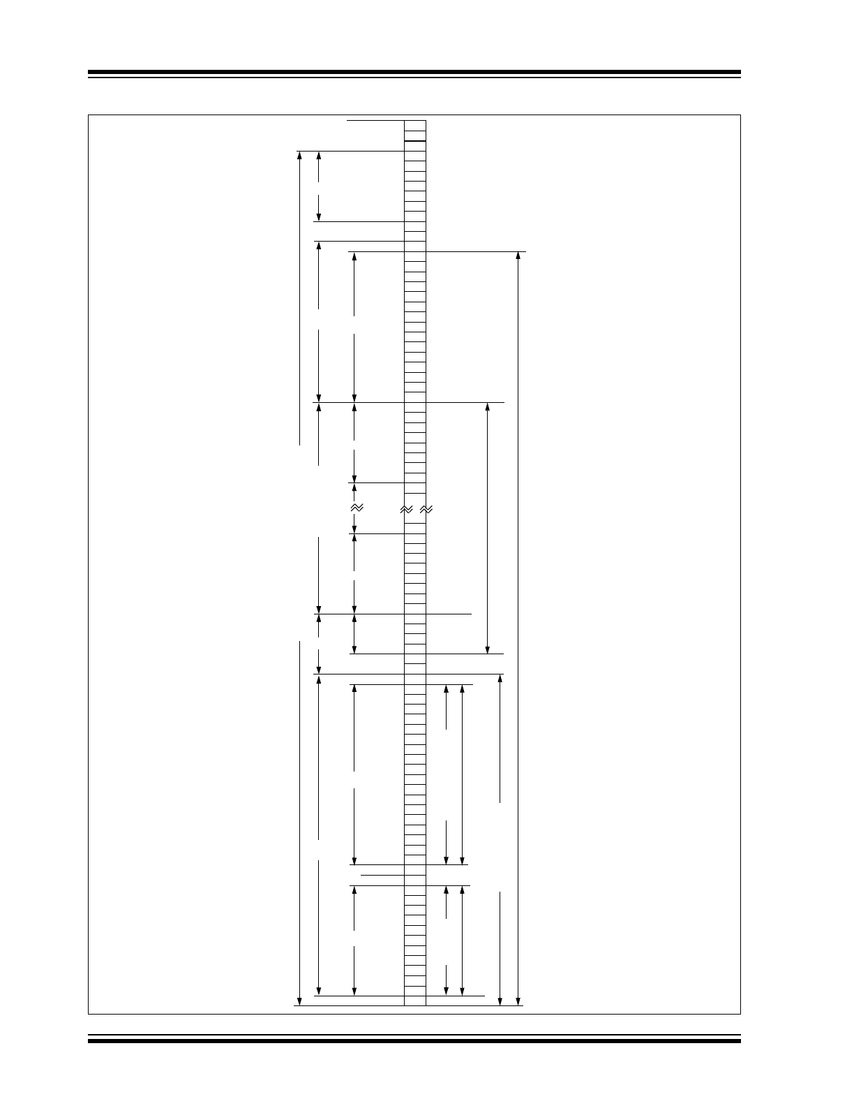
Extended Data Frame
In the extended CAN data frame, shown in
Figure 2-2
,
the SOF bit is followed by the arbitration field, which
consists of 32 bits. The first 11 bits are the Most
Significant bits (MSb) (Base-lD) of the 29-bit identifier.
These 11 bits are followed by the Substitute Remote
Request (SRR) bit, which is defined to be recessive.
The SRR bit is followed by the lDE bit, which is
recessive to denote an extended CAN frame.
It should be noted that if arbitration remains unresolved
after transmission of the first 11 bits of the identifier, and
one of the nodes involved in the arbitration is sending
a standard CAN frame (11-bit identifier), the standard
CAN frame will win arbitration due to the assertion of a
dominant lDE bit. Also, the SRR bit in an extended
CAN frame must be recessive to allow the assertion of
a dominant RTR bit by a node that is sending a
standard CAN remote frame.
The SRR and lDE bits are followed by the remaining
18 bits of the identifier (Extended lD) and the Remote
Transmission Request bit.
To enable standard and extended frames to be sent
across a shared network, the 29-bit extended message
identifier is split into 11-bit (Most Significant) and 18-bit
(Least Significant) sections. This split ensures that the
lDE bit can remain at the same bit position in both the
standard and extended frames.
Following the arbitration field is the six-bit control field.
The first two bits of this field are reserved and must be
dominant. The remaining four bits of the control field
are the DLC, which specifies the number of data bytes
contained in the message.
The remaining portion of the frame (data field, CRC
field, Acknowledge field, End-of-Frame and intermis-
sion) is constructed in the same way as a standard data
frame (see
Section 2.1 “Standard Data Frame”
).
2.3
Remote Frame
Normally, data transmission is performed on an
autonomous basis by the data source node (e.g., a
sensor sending out a data frame). It is possible,
however, for a destination node to request data from the
source. To accomplish this, the destination node sends
a remote frame with an identifier that matches the iden-
tifier of the required data frame. The appropriate data
source node will then send a data frame in response to
the remote frame request.
There are two differences between a remote frame
(shown in
Figure 2-3
) and a data frame. First, the RTR
bit is at the recessive state, and second, there is no
data field. In the event of a data frame and a remote
frame with the same identifier being transmitted at the
same time, the data frame wins arbitration due to the
dominant RTR bit following the identifier. In this way,
the node that transmitted the remote frame receives
the desired data immediately.
2.4
Error Frame
An error frame is generated by any node that detects a
bus error. An error frame, shown in
Figure 2-4
, consists
of two fields: an error flag field followed by an error
delimiter field. There are two types of error flag fields.
The type of error flag field sent depends upon the error
status of the node that detects and generates the error
flag field.

MCP2515
DS20001801H-page 8
2003-2016 Microchip Technology Inc.
2.4.1
ACTIVE ERRORS
If an error-active node detects a bus error, the node
interrupts transmission of the current message by
generating an active error flag. The active error flag is
composed of six consecutive dominant bits. This bit
sequence actively violates the bit-stuffing rule. All other
stations recognize the resulting bit-stuffing error, and in
turn, generate error frames themselves, called error
echo flags.
The error flag field, therefore, consists of between six
and twelve consecutive dominant bits (generated by
one or more nodes). The error delimiter field (eight
recessive bits) completes the error frame. Upon
completion of the error frame, bus activity returns to
normal and the interrupted node attempts to resend the
aborted message.
2.4.2
PASSIVE ERRORS
If an error-passive node detects a bus error, the node
transmits an error-passive flag followed by the error
delimiter field. The error-passive flag consists of six
consecutive recessive bits. The error frame for an error-
passive node consists of 14 recessive bits. From this, it
follows that unless the bus error is detected by an error-
active node or the transmitting node, the message will
continue transmission because the error-passive flag
does not interfere with the bus.
If the transmitting node generates an error-passive flag,
it will cause other nodes to generate error frames due to
the resulting bit-stuffing violation. After transmission of
an error frame, an error-passive node must wait for six
consecutive recessive bits on the bus before attempting
to rejoin bus communications.
The error delimiter consists of eight recessive bits, and
allows the bus nodes to restart bus communications
cleanly after an error has occurred.
2.5
Overload Frame
An overload frame, shown in
Figure 2-5
, has the same
format as an active-error frame. An overload frame,
however, can only be generated during an interframe
space. In this way, an overload frame can be
differentiated from an error frame (an error frame is
sent during the transmission of a message). The
overload frame consists of two fields: an overload flag
followed by an overload delimiter. The overload flag
consists of six dominant bits followed by overload flags
generated by other nodes (and, as for an active error
flag, giving a maximum of twelve dominant bits). The
overload delimiter consists of eight recessive bits. An
overload frame can be generated by a node as a result
of two conditions:
1.
The node detects a dominant bit during the inter-
frame space, an illegal condition. Exception: The
dominant bit is detected during the third bit of IFS.
In this case, the receivers will interpret this as a
SOF.
2.
Due to internal conditions, the node is not yet
able to begin reception of the next message. A
node may generate a maximum of two sequential
overload frames to delay the start of the next
message.
2.6
Interframe Space
The interframe space separates a preceding frame (of
any type) from a subsequent data or remote frame.
The interframe space is composed of at least three
recessive bits, called the ‘Intermission’. This allows
nodes time for internal processing before the start of
the next message frame. After the intermission, the
bus line remains in the recessive state (Bus Idle) until
the next transmission starts.
Note:
Error echo flags typically occur when a
localized disturbance causes one or more
(but not all) nodes to send an error flag.
The remaining nodes generate error flags
in response (echo) to the original error flag.
Note:
Case 2 should never occur with the
MCP2515 due to very short internal
delays.
2003-2016 Microchip Technology Inc.
DS20001801H-page 9
MCP2515
FIGURE 2-1:
STANDARD DATA FRAME
0
0
0
0
1
1
1
1
1
1
1
1
Start
-of
-Fram
e
Dat
a
F
rame (num
ber of
bit
s
=
44 +
8N
)
12
A
rbit
ra
tion F
ield
ID 1
0
11
ID3
ID0
Ident
if
ier
Mes
s
age
F
iltering
S
tored i
n
Buf
fe
rs
RTR
IDE
RB0
DLC3
DLC0
6
4
Cont
rol
Fie
ld
Dat
a
Lengt
h
Code
Re
served B
it
8N (0
N
8)
Dat
a
F
ield
8
8
S
tored in
T
rans
mit
/Rec
e
iv
e B
u
ff
ers
Bi
t-
S
tu
ffi
n
g
16
CRC F
ield
15
CRC
7
E
nd-of
-
Fr
a
m
e
CRC Del
Ack Sl
ot B
it
ACK
De
l
IFS
1
1
1
1
MCP2515
DS20001801H-page 10
2003-2016 Microchip Technology Inc.
FIGURE 2-2:
EXTENDED DATA FRAME
0
1
1
00
0
1
Start
-of
-Fra
me
Arb
it
rat
ion F
iel
d
32
11
ID1
0
ID3
ID0
IDE
Ident
if
ier
Mes
s
age
Filt
ering
S
tore
d
in B
u
ff
ers
SRR
EID
17
EID
0
RTR
RB1
RB0
DLC3
18
DLC0
6
Cont
ro
l
Fi
e
ld
4
Reserved B
its
Dat
a
Lengt
h
Code
S
to
red in
T
rans
mit
/Receiv
e B
u
ff
er
s
8
8
Dat
a
F
rame (num
ber of
bi
ts
=
64 +
8N
)
8N
(0
N
8)
D
a
ta
F
ie
ld
11
1
1
1
1
1
1
16
CRC F
ield
15
CRC
CRC Del
Ack Sl
ot B
it
ACK
De
l
E
nd-of
-
Fr
a
m
e
7
Bi
t-
S
tu
ffin
g
IF
S
Exte
n
d
e
d
Id
e
n
ti
fie
r
1
1
1