
©
2007 Microchip Technology Inc.
DS21291F-page 1
MCP2510
Features
• Implements Full CAN V2.0A and V2.0B at 1 Mb/s:
- 0 - 8 byte message length
- Standard and extended data frames
- Programmable bit rate up to 1 Mb/s
- Support for remote frames
- Two receive buffers with prioritized message
storage
- Six full acceptance filters
- Two full acceptance filter masks
- Three transmit buffers with prioritization and
abort features
- Loop-back mode for self test operation
• Hardware Features:
- High Speed SPI Interface
(5 MHz at 4.5V I temp)
- Supports SPI modes 0,0 and 1,1
- Clock out pin with programmable prescaler
- Interrupt output pin with selectable enables
- ‘Buffer full’ output pins configureable as inter-
rupt pins for each receive buffer or as general
purpose digital outputs
- ‘Request to Send’ input pins configureable as
control pins to request immediate message
transmission for each transmit buffer or as
general purpose digital inputs
- Low Power Sleep mode
• Low power CMOS technology:
- Operates from 3.0V to 5.5V
- 5 mA active current typical
- 10 µA standby current typical at 5.5V
• 18-pin PDIP/SOIC and 20-pin TSSOP packages
• Temperature ranges supported:
Description
The Microchip Technology Inc. MCP2510 is a Full Con-
troller Area Network (CAN) protocol controller imple-
menting CAN specification V2.0 A/B. It supports CAN
1.2, CAN 2.0A, CAN 2.0B Passive, and CAN 2.0B
Active versions of the protocol, and is capable of trans-
mitting and receiving standard and extended mes-
sages. It is also capable of both acceptance filtering
and message management. It includes three transmit
buffers and two receive buffers that reduce the amount
of microcontroller (MCU) management required. The
MCU communication is implemented via an industry
standard Serial Peripheral Interface (SPI) with data
rates up to 5 Mb/s.
Package Types
- Industrial (I):
-40°C to +85°C
- Extended (E):
-40°C to +125°C
TXCAN
RXCAN
V
DD
RESET
CS
SO
MC
P
2
51
0
1
2
3
4
18
17
16
15
SI
SCK
INT
RX0BF
14
13
12
11
RX1BF
10
OSC2
OSC1
CLKOUT
TX2RTS
5
6
7
8
V
SS
9
MC
P
2
51
0
TXCAN
RXCAN
TX0RTS
OSC1
CLKOUT
OSC2
CS
V
DD
RESET
SO
SCK
INT
SI
RX0BF
RX1BF
V
SS
TX0RTS
TX1RTS
TX1RTS
TX2RTS
NC
NC
13
12
1
2
3
4
5
6
7
8
9
20
19
18
17
16
15
14
11
10
18 LEAD PDIP/SOIC
20 LEAD TSSOP
Stand-Alone CAN Controller with SPI
™
Interface

MCP2510
DS21291F-page 2
©
2007 Microchip Technology Inc.
Table of Contents
1.0
Device Functionality . . . . . . . . . . . . . . . . . . . . . . . . . . . . . . . . . . . . . . . . . . . . . . . . . . . . . . . . . . . . . . . . . . . . . . . . . . . . . . . 3
2.0
Can Message Frames. . . . . . . . . . . . . . . . . . . . . . . . . . . . . . . . . . . . . . . . . . . . . . . . . . . . . . . . . . . . . . . . . . . . . . . . . . . . . . 7
3.0
Message Transmission . . . . . . . . . . . . . . . . . . . . . . . . . . . . . . . . . . . . . . . . . . . . . . . . . . . . . . . . . . . . . . . . . . . . . . . . . . . . 15
4.0
Message Reception . . . . . . . . . . . . . . . . . . . . . . . . . . . . . . . . . . . . . . . . . . . . . . . . . . . . . . . . . . . . . . . . . . . . . . . . . . . . . . 21
5.0
Bit Timing . . . . . . . . . . . . . . . . . . . . . . . . . . . . . . . . . . . . . . . . . . . . . . . . . . . . . . . . . . . . . . . . . . . . . . . . . . . . . . . . . . . . . . 35
6.0
Error Detection . . . . . . . . . . . . . . . . . . . . . . . . . . . . . . . . . . . . . . . . . . . . . . . . . . . . . . . . . . . . . . . . . . . . . . . . . . . . . . . . . . 41
7.0
Interrupts. . . . . . . . . . . . . . . . . . . . . . . . . . . . . . . . . . . . . . . . . . . . . . . . . . . . . . . . . . . . . . . . . . . . . . . . . . . . . . . . . . . . . . . 45
8.0
Oscillator . . . . . . . . . . . . . . . . . . . . . . . . . . . . . . . . . . . . . . . . . . . . . . . . . . . . . . . . . . . . . . . . . . . . . . . . . . . . . . . . . . . . . . . 49
9.0
Modes of Operation . . . . . . . . . . . . . . . . . . . . . . . . . . . . . . . . . . . . . . . . . . . . . . . . . . . . . . . . . . . . . . . . . . . . . . . . . . . . . . 51
10.0
Register Map. . . . . . . . . . . . . . . . . . . . . . . . . . . . . . . . . . . . . . . . . . . . . . . . . . . . . . . . . . . . . . . . . . . . . . . . . . . . . . . . . . . . 55
11.0
SPI Interface . . . . . . . . . . . . . . . . . . . . . . . . . . . . . . . . . . . . . . . . . . . . . . . . . . . . . . . . . . . . . . . . . . . . . . . . . . . . . . . . . . . . 57
12.0
Electrical Characteristics. . . . . . . . . . . . . . . . . . . . . . . . . . . . . . . . . . . . . . . . . . . . . . . . . . . . . . . . . . . . . . . . . . . . . . . . . . . 61
13.0
Packaging Information . . . . . . . . . . . . . . . . . . . . . . . . . . . . . . . . . . . . . . . . . . . . . . . . . . . . . . . . . . . . . . . . . . . . . . . . . . . . 65
Index . . . . . . . . . . . . . . . . . . . . . . . . . . . . . . . . . . . . . . . . . . . . . . . . . . . . . . . . . . . . . . . . . . . . . . . . . . . . . . . . . . . . . . . . . . . . . . . . . . 69
On-Line Support . . . . . . . . . . . . . . . . . . . . . . . . . . . . . . . . . . . . . . . . . . . . . . . . . . . . . . . . . . . . . . . . . . . . . . . . . . . . . . . . . . . . . . . . . 71
Reader Response . . . . . . . . . . . . . . . . . . . . . . . . . . . . . . . . . . . . . . . . . . . . . . . . . . . . . . . . . . . . . . . . . . . . . . . . . . . . . . . . . . . . . . . . 72
Product Identification System . . . . . . . . . . . . . . . . . . . . . . . . . . . . . . . . . . . . . . . . . . . . . . . . . . . . . . . . . . . . . . . . . . . . . . . . . . . . . . . 73
Worldwide Sales and Service . . . . . . . . . . . . . . . . . . . . . . . . . . . . . . . . . . . . . . . . . . . . . . . . . . . . . . . . . . . . . . . . . . . . . . . . . . . . . . . 76
TO OUR VALUED CUSTOMERS
It is our intention to provide our valued customers with the best documentation possible to ensure successful use of your Micro-
chip products. To this end, we will continue to improve our publications to better suit your needs. Our publications will be refined
and enhanced as new volumes and updates are introduced.
If you have any questions or comments regarding this publication, please contact the Marketing Communications Department via
E-mail at docerrors@microchip.com or fax the Reader Response Form in the back of this data sheet to (480) 792-4150. We
welcome your feedback.
Most Current Data Sheet
To obtain the most up-to-date version of this data sheet, please register at our Worldwide Web site at:
http://www.microchip.com
You can determine the version of a data sheet by examining its literature number found on the bottom outside corner of any page.
The last character of the literature number is the version number, (e.g., DS30000A is version A of document DS30000).
Errata
An errata sheet, describing minor operational differences from the data sheet and recommended workarounds, may exist for cur-
rent devices. As device/documentation issues become known to us, we will publish an errata sheet. The errata will specify the revi-
sion of silicon and revision of document to which it applies.
To determine if an errata sheet exists for a particular device, please check with one of the following:
• Microchip’s Worldwide Web site; http://www.microchip.com
• Your local Microchip sales office (see last page)
When contacting a sales office, please specify which device, revision of silicon and data sheet (include literature number) you are
using.
Customer Notification System
Register on our web site at www.microchip.com to receive the most current information on all of our products.
©
2007 Microchip Technology Inc.
DS21291F-page 3
MCP2510
1.0
DEVICE FUNCTIONALITY
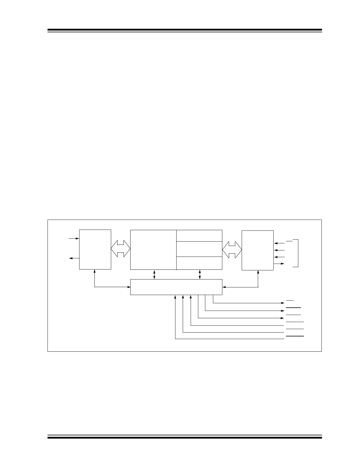
1.1
Overview
The MCP2510 is a stand-alone CAN controller devel-
oped to simplify applications that require interfacing
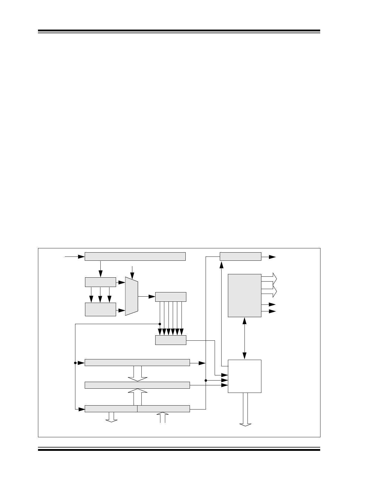
with a CAN bus. A simple block diagram of the
MCP2510 is shown in Figure 1-1. The device consists
of three main blocks:
1.
The CAN protocol engine.
2.
The control logic and SRAM registers that are
used to configure the device and its operation.
3.
The SPI protocol block.
A typical system implementation using the device is
shown in Figure 1-2.
The CAN protocol engine handles all functions for
receiving and transmitting messages on the bus. Mes-
sages are transmitted by first loading the appropriate
message buffer and control registers. Transmission is
initiated by using control register bits, via the SPI inter-
face, or by using the transmit enable pins. Status and
errors can be checked by reading the appropriate reg-
isters. Any message detected on the CAN bus is
checked for errors and then matched against the user
defined filters to see if it should be moved into one of
the two receive buffers.
The MCU interfaces to the device via the SPI interface.
Writing to and reading from all registers is done using
standard SPI read and write commands.
Interrupt pins are provided to allow greater system flex-
ibility. There is one multi-purpose interrupt pin as well
as specific interrupt pins for each of the receive regis-
ters that can be used to indicate when a valid message
has been received and loaded into one of the receive
buffers. Use of the specific interrupt pins is optional,
and the general purpose interrupt pin as well as status
registers (accessed via the SPI interface) can also be
used to determine when a valid message has been
received.
There are also three pins available to initiate immediate
transmission of a message that has been loaded into
one of the three transmit registers. Use of these pins is
optional and initiating message transmission can also
be done by utilizing control registers accessed via the
SPI interface.
Table 1-1 gives a complete list of all of the pins on the
MCP2510.
FIGURE 1-1:
BLOCK DIAGRAM
3 TX
Buffers
2 RX Buffers
Message Assembly
6 Acceptance
Filters
SPI
Interface
Logic
SPI
Bus
INT
Buffer
CS
SCK
SI
SO
CAN
Protocol
Engine
RXCAN
TXCAN
Control Logic
RX0BF
RX1BF
TX0RTS
TX1RTS
TX2RTS
MCP2510
DS21291F-page 4
©
2007 Microchip Technology Inc.
FIGURE 1-2:
TYPICAL SYSTEM IMPLEMENTATION
TABLE 1-1:
PIN DESCRIPTIONS
Name
DIP/
SOIC
Pin #
TSSOP
Pin #
I/O/P
Type
Description
TXCAN
1
1
O
Transmit output pin to CAN bus
RXCAN
2
2
I
Receive input pin from CAN bus
CLKOUT
3
3
O
Clock output pin with programmable prescaler
TX0RTS
4
4
I
Transmit buffer TXB0 request to send or general purpose digital input. 100 k
Ω
internal pullup to V
DD
TX1RTS
5
5
I
Transmit buffer TXB1 request to send or general purpose digital input. 100 k
Ω
internal pullup to V
DD
TX2RTS
6
7
I
Transmit buffer TXB2 request to send or general purpose digital input. 100 k
Ω
internal pullup to V
DD
OSC2
7
8
O
Oscillator output
OSC1
8
9
I
Oscillator input
V
SS
9
10
P
Ground reference for logic and I/O pins
RX1BF
10
11
O
Receive buffer RXB1 interrupt pin or general purpose digital output
RX0BF
11
12
O
Receive buffer RXB0 interrupt pin or general purpose digital output
INT
12
13
O
Interrupt output pin
SCK
13
14
I
Clock input pin for SPI interface
SI
14
16
I
Data input pin for SPI interface
SO
15
17
O
Data output pin for SPI interface
CS
16
18
I
Chip select input pin for SPI interface
RESET
17
19
I
Active low device reset input
V
DD
18
20
P
Positive supply for logic and I/O pins
NC
—
6,15
—
No internal connection
Note:
Type Identification: I=Input; O=Output; P=Power
MCP2510
SPI
MCP2510
MCP2510
MCP2510
INTERFACE
CAN
BUS
MCP2510
Main
System
Controller
CAN
Transceiver
CAN
Transceiver
CAN
Transceiver
CAN
Transceiver
CAN
Transceiver
Node
Controller
Node
Controller
Node
Controller
Node
Controller
©
2007 Microchip Technology Inc.
DS21291F-page 5
MCP2510
1.2
Transmit/Receive Buffers
The MCP2510 has three transmit and two receive buffers, two acceptance masks (one for each receive buffer), and a
total of six acceptance filters. Figure 1-3 is a block diagram of these buffers and their connection to the protocol engine.
FIGURE 1-3:
CAN BUFFERS AND PROTOCOL ENGINE BLOCK DIAGRAM
Acceptance Filter
RXF2
R
X
B
1
Identifier
Data Field
Data Field
Identifier
Acceptance Mask
RXM1
Acceptance Filter
RXF3
Acceptance Filter
RXF4
Acceptance Filter
RXF5
M
A
B
Acceptance Filter
RXF0
Acceptance Filter
RXF1
R
X
B
0
TX
R
E
Q
TXB2
ABT
F
ML
O
A
TX
ERR
ME
SS
AGE
Message
Queue
Control
Transmit Byte Sequencer
TX
R
E
Q
TXB0
ABT
F
ML
O
A
TX
ERR
ME
SS
AGE
CRC<14:0>
Comparator
Receive<7:0>
Transmit<7:0>
Receive
Error
Transmit
Error
Protocol
REC
TEC
ErrPas
BusOff
Finite
State
Machine
Counter
Counter
Shift<14:0>
{Transmit<5:0>, Receive<8:0>}
Transmit
Logic
Bit
Timing
Logic
TX
RX
Configuration
Registers
Clock
Generator
PROTOCOL
ENGINE
BUFFERS
TX
R
E
Q
TXB1
ABT
F
ML
O
A
TX
ERR
ME
SS
AGE
Acceptance Mask
RXM0
A
c
c
e
p
t
A
c
c
e
p
t
MCP2510
DS21291F-page 6
©
2007 Microchip Technology Inc.
1.3
CAN Protocol Engine
The CAN protocol engine combines several functional
blocks, shown in Figure 1-4. These blocks and their
functions are described below.
1.4
Protocol Finite State Machine
The heart of the engine is the Finite State Machine
(FSM). This state machine sequences through mes-
sages on a bit by bit basis, changing states as the fields
of the various frame types are transmitted or received.
The FSM is a sequencer controlling the sequential data
stream between the TX/RX Shift Register, the CRC
Register, and the bus line. The FSM also controls the
Error Management Logic (EML) and the parallel data
stream between the TX/RX Shift Registers and the
buffers. The FSM insures that the processes of recep-
tion, arbitration, transmission, and error signaling are
performed according to the CAN protocol. The auto-
matic retransmission of messages on the bus line is
also handled by the FSM.
1.5
Cyclic Redundancy Check
The Cyclic Redundancy Check Register generates the
Cyclic Redundancy Check (CRC) code which is trans-
mitted after either the Control Field (for messages with
0 data bytes) or the Data Field, and is used to check the
CRC field of incoming messages.
1.6
Error Management Logic
The Error Management Logic is responsible for the
fault confinement of the CAN device. Its two counters,
the Receive Error Counter (REC) and the Transmit
Error Counter (TEC), are incremented and decre-
mented by commands from the Bit Stream Processor.
According to the values of the error counters, the CAN
controller is set into the states error-active, error-pas-
sive or bus-off.
1.7
Bit Timing Logic
The Bit Timing Logic (BTL) monitors the bus line input
and handles the bus related bit timing according to the
CAN protocol. The BTL synchronizes on a recessive to
dominant bus transition at Start of Frame (hard syn-
chronization) and on any further recessive to dominant
bus line transition if the CAN controller itself does not
transmit a dominant bit (resynchronization). The BTL
also provides programmable time segments to com-
pensate for the propagation delay time, phase shifts,
and to define the position of the Sample Point within the
bit time. The programming of the BTL depends upon
the baud rate and external physical delay times.
FIGURE 1-4:
CAN PROTOCOL ENGINE BLOCK DIAGRAM
Bit Timing Logic
CRC<14:0>
Comparator
Receive<7:0>
Transmit<7:0>
Sample<2:0>
Majority
Decision
StuffReg<5:0>
Comparator
Transmit Logic
Receive
Error Counter
Transmit
Error Counter
Protocol
FSM
RX
SAM
BusMon
Rec/Trm Addr.
RecData<7:0>
TrmData<7:0>
Shift<14:0>
(Transmit<5:0>, Receive<7:0>)
TX
REC
TEC
ErrPas
BusOff
Interface to Standard Buffer

©
2007 Microchip Technology Inc.
DS21291F-page 7
MCP2510
2.0
CAN MESSAGE FRAMES
The MCP2510 supports Standard Data Frames,
Extended Data Frames, and Remote Frames (Stan-
dard and Extended) as defined in the CAN 2.0B speci-
fication.
2.1
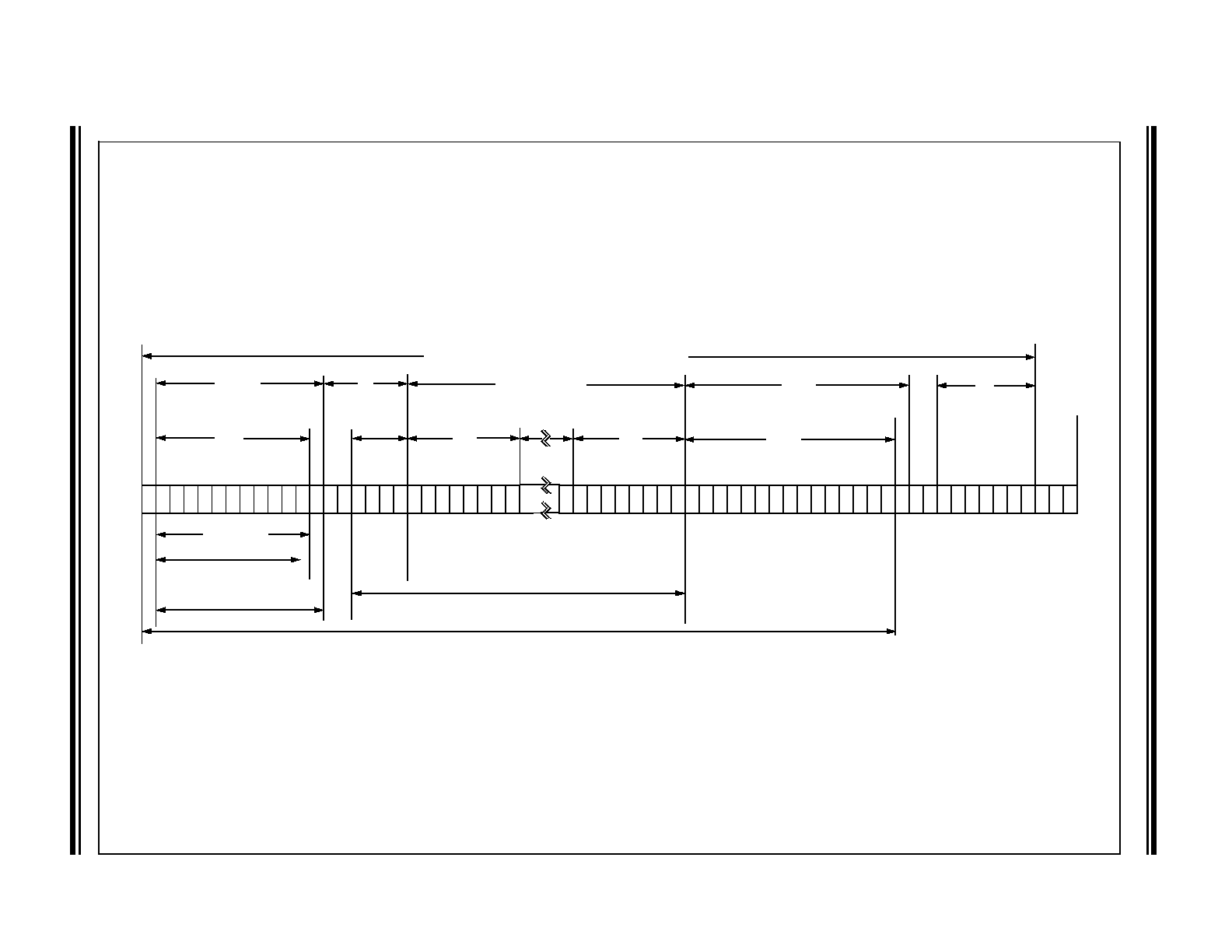
Standard Data Frame
The CAN Standard Data Frame is shown in Figure 2-1.
In common with all other frames, the frame begins with
a Start Of Frame (SOF) bit, which is of the dominant
state, which allows hard synchronization of all nodes.
The SOF is followed by the arbitration field, consisting
of 12 bits; the 11-bit ldentifier and the Remote Trans-
mission Request (RTR) bit. The RTR bit is used to dis-
tinguish a data frame (RTR bit dominant) from a remote
frame (RTR bit recessive).
Following the arbitration field is the control field, con-
sisting of six bits. The first bit of this field is the Identifier
Extension (IDE) bit which must be dominant to specify
a standard frame. The following bit, Reserved Bit Zero
(RB0), is reserved and is defined to be a dominant bit
by the can protocol. the remaining four bits of the con-
trol field are the Data Length Code (DLC) which speci-
fies the number of bytes of data contained in the
message.
After the control field is the data field, which contains
any data bytes that are being sent, and is of the length
defined by the DLC above (0-8 bytes).
The Cyclic Redundancy Check (CRC) Field follows the
data field and is used to detect transmission errors. The
CRC Field consists of a 15-bit CRC sequence, followed
by the recessive CRC Delimiter bit.
The final field is the two-bit acknowledge field. During
the ACK Slot bit, the transmitting node sends out a
recessive bit. Any node that has received an error free
frame acknowledges the correct reception of the frame
by sending back a dominant bit (regardless of whether
the node is configured to accept that specific message
or not). The recessive acknowledge delimiter com-
pletes the acknowledge field and may not be overwrit-
ten by a dominant bit.
2.2
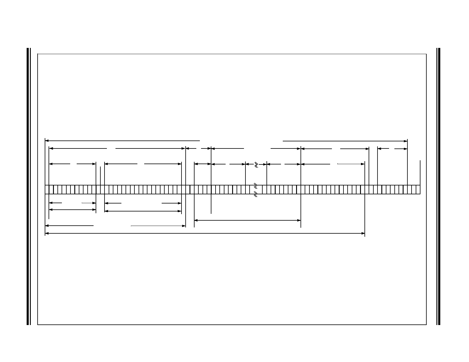
Extended Data Frame
In the Extended CAN Data Frame, the SOF bit is fol-
lowed by the arbitration field which consists of 32 bits,
as shown in Figure 2-2. The first 11 bits are the most
significant bits (Base-lD) of the 29-bit identifier. These
11 bits are followed by the Substitute Remote Request
(SRR) bit which is defined to be recessive. The SRR bit
is followed by the lDE bit which is recessive to denote
an extended CAN frame.
It should be noted that if arbitration remains unresolved
after transmission of the first 11 bits of the identifier, and
one of the nodes involved in the arbitration is sending
a standard CAN frame (11-bit identifier), then the stan-
dard CAN frame will win arbitration due to the assertion
of a dominant lDE bit. Also, the SRR bit in an extended
CAN frame must be recessive to allow the assertion of
a dominant RTR bit by a node that is sending a stan-
dard CAN remote frame.
The SRR and lDE bits are followed by the remaining 18
bits of the identifier (Extended lD) and the remote trans-
mission request bit.
To enable standard and extended frames to be sent
across a shared network, it is necessary to split the 29-
bit extended message identifier into 11-bit (most signif-
icant) and 18-bit (least significant) sections. This split
ensures that the lDE bit can remain at the same bit
position in both standard and extended frames.
Following the arbitration field is the six-bit control field.
the first two bits of this field are reserved and must be
dominant. the remaining four bits of the control field are
the Data Length Code (DLC) which specifies the num-
ber of data bytes contained in the message.
The remaining portion of the frame (data field, CRC
field, acknowledge field, end of frame and lntermission)
is constructed in the same way as for a standard data
frame (see Section 2.1).
2.3
Remote Frame
Normally, data transmission is performed on an auton-
omous basis by the data source node (e.g. a sensor
sending out a data frame). It is possible, however, for a
destination node to request data from the source. To
accomplish this, the destination node sends a remote
frame with an identifier that matches the identifier of the
required data frame. The appropriate data source node
will then send a data frame in response to the remote
frame request.
There are two differences between a remote frame
(shown in Figure 2-3) and a data frame. First, the RTR
bit is at the recessive state, and second, there is no
data field. In the event of a data frame and a remote
frame with the same identifier being transmitted at the
same time, the data frame wins arbitration due to the
dominant RTR bit following the identifier. In this way,
the node that transmitted the remote frame receives
the desired data immediately.
2.4
Error Frame
An Error Frame is generated by any node that detects
a bus error. An error frame, shown in Figure 2-4, con-
sists of two fields, an error flag field followed by an error
delimiter field. There are two types of error flag fields.
Which type of error flag field is sent depends upon the
error status of the node that detects and generates the
error flag field.
If an error-active node detects a bus error then the
node interrupts transmission of the current message by
generating an active error flag. The active error flag is
composed of six consecutive dominant bits. This bit

MCP2510
DS21291F-page 8
©
2007 Microchip Technology Inc.
sequence actively violates the bit stuffing rule. All other
stations recognize the resulting bit stuffing error and in
turn generate error frames themselves, called error
echo flags. The error flag field, therefore, consists of
between six and twelve consecutive dominant bits
(generated by one or more nodes). The error delimiter
field completes the error frame. After completion of the
error frame, bus activity returns to normal and the inter-
rupted node attempts to resend the aborted message.
If an error-passive node detects a bus error then the
node transmits an error-passive flag followed by the
error delimiter field. The error-passive flag consists of
six consecutive recessive bits, and the error frame for
an error-passive node consists of 14 recessive bits.
From this, it follows that unless the bus error is
detected by the node that is actually transmitting, the
transmission of an error frame by an error-passive
node will not affect any other node on the network. If
the transmitting node generates an error-passive flag
then this will cause other nodes to generate error
frames due to the resulting bit stuffing violation. After
transmission of an error frame, an error-passive node
must wait for six consecutive recessive bits on the bus
before attempting to rejoin bus communications.
The error delimiter consists of eight recessive bits and
allows the bus nodes to restart bus communications
cleanly after an error has occurred.
2.5
Overload Frame
An Overload Frame, shown in Figure 2-5, has the
same format as an active error frame. An overload
frame, however can only be generated during an lnter-
frame space. In this way an overload frame can be dif-
ferentiated from an error frame (an error frame is sent
during the transmission of a message). The overload
frame consists of two fields, an overload flag followed
by an overload delimiter. The overload flag consists of
six dominant bits followed by overload flags generated
by other nodes (and, as for an active error flag, giving
a maximum of twelve dominant bits). The overload
delimiter consists of eight recessive bits. An overload
frame can be generated by a node as a result of two
conditions. First, the node detects a dominant bit during
the interframe space which is an illegal condition. Sec-
ond, due to internal conditions the node is not yet able
to start reception of the next message. A node may
generate a maximum of two sequential overload
frames to delay the start of the next message.
2.6
Interframe Space
The lnterframe Space separates a preceeding frame
(of any type) from a subsequent data or remote frame.
The interframe space is composed of at least three
recessive bits called the Intermission. This is provided
to allow nodes time for internal processing before the
start of the next message frame. After the intermission,
the bus line remains in the recessive state (bus idle)
until the next transmission starts.
©
2007
Micr
ochip T
e
ch
nol
ogy
I
n
c.
DS
21291F
-page 9
MCP2
510
FIGURE 2-1:
STANDARD DATA FRAME
0
S
ta
rt
of
F
rame
Data Frame (number of bits = 44 + 8N)
12
Arbitration Field
ID 1
0
11
ID3
ID0
Identifier
Message
Filtering
Stored in Buffers
RTR
ID
E
RB
0
DLC
3
DL
C0
6
4
Control
Field
Data
Length
Code
Reserv
ed B
it
8N (0
≤
N
≤
8)
Data Field
8
8
Stored in Transmit/Receive Buffers
Bit Stuffing
16
CRC Field
15
CRC
7
End of
Frame
C
RC De
l
A
ck Sl
ot Bi
t
AC
K
D
e
l
IFS
0 0 0
1
1 1 1 1 1 1 1 1 1 1 1
©
2007
Micr
ochip T
e
ch
nol
ogy
I
n
c.
DS
21291F
-page 10
MCP2
510
FIGURE 2-2:
EXTENDED DATA FRAME
0
1 1
0 0 0
1
S
tar
t of
F
rame
Arbitration Field
32
11
ID1
0
ID3
ID
0
ID
E
Identifier
Message
Filtering
Stored in Buffers
SR
R
EI
D
1
7
EI
D
0
RTR RB
1
RB
0
DLC3
18
DLC0
6
Control
Field
4
Res
e
rved bit
s
Data
Length
Code
Stored in Transmit/Receive Buffers
8
8
Data Frame (number of bits = 64 + 8N)
8N (0
≤
N
≤
8)
Data Field
1 1 1 1 1 1 1 1
16
CRC Field
15
CRC
CRC
Del
Ac
k S
lot
Bi
t
AC
K
D
e
l
End of
Frame
7
Bit Stuffing
IFS
Extended Identifier
1 1 1