
2001 Microchip Technology Inc.
DS20072A-page 1
M
MCP2505X
This document includes the programming
specifications for the following devices:
• MCP25050
• MCP25055
1.0
OVERVIEW
This specification describes the requirements to pro-
gram a device. Programming is accomplished through
a serial interface. A serial interface reduces the number
of device pins that must be controlled and eases the
application requirements for the device to be pro-
grammed while in the users system. This capability
increases design flexibility, and is referred to as In-Cir-
cuit Serial Programming™ (ICSP™).
1.1
Hardware Requirements
The MCP2505X requires two programmable power
supplies, one for V
DD
(2.0V to 6.0V recommended) and
one for V
PP
(12V to 14V). Both supplies should have a
minimum resolution of 0.25V.
1.2
Programming Mode
The programming mode for the MCP2505X allows pro-
gramming of user program memory and the configura-
tion word.
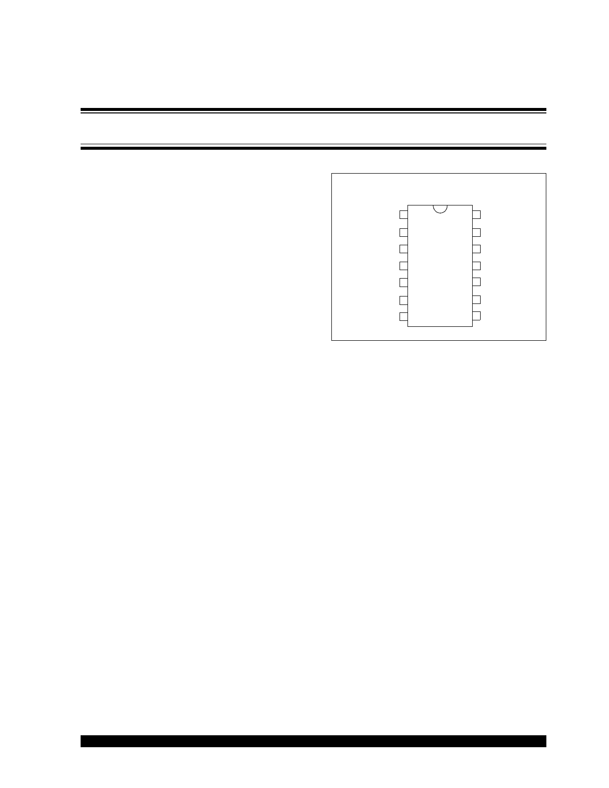
PACKAGE TYPES:
PDIP/SOIC
GP0/AN0
GP1/AN1
V
DD
TXCAN/TXRXCAN
RXCAN/NC
GP5/V
REF
+/CLOCK
1
2
3
4
GP4/V
REF
-/DATA
GP6/CLKOUT
14
13
12
11
10
GP3/AN3/PWM2
OSC1/CLKIN
GP2/AN2/PWM1
5
6
7
8
9
OSC2
V
SS
GP7/RST/V
PP
MCP
25055
MCP
25050
Programming Specifications
MCP2505X
DS20072A-page 2
2001 Microchip Technology Inc.
2.0
MCP2505X MEMORY
The MCP2505X has two memory spaces. The first is
the User EPROM Memory. This memory stores the
default configuration values for the device. The second
memory space is the configuration memory. This con-
tains the values for the device oscillator and reset pin
configurations.
2.1
User EPROM Memory Map
The User EPROM memory space extends from 0x00 to
0x45. Table 2-1 shows this program memory map.
This User EPROM memory is offset within the device
memory map. When programming the device, an offset
to the addresses in Table 2-1 is required.
2.2
Configuration Memory
Configuration memory is accessed with the Load Con-
figuration command. Once in configuration memory,
the only way to access the User EPROM Memory is to
reset the device and re-enter Programming mode, as
described in Section 3.1. Only the lower 3 bits should
be programmed. The remaining 11 bits are reserved
and should be programmed as a ‘1’. Programming
these bits as a ‘1’ will ensure that the factory value is
not modified. When verifying this location, only verify
against the lower 3 bits (the bits that were pro-
grammed).
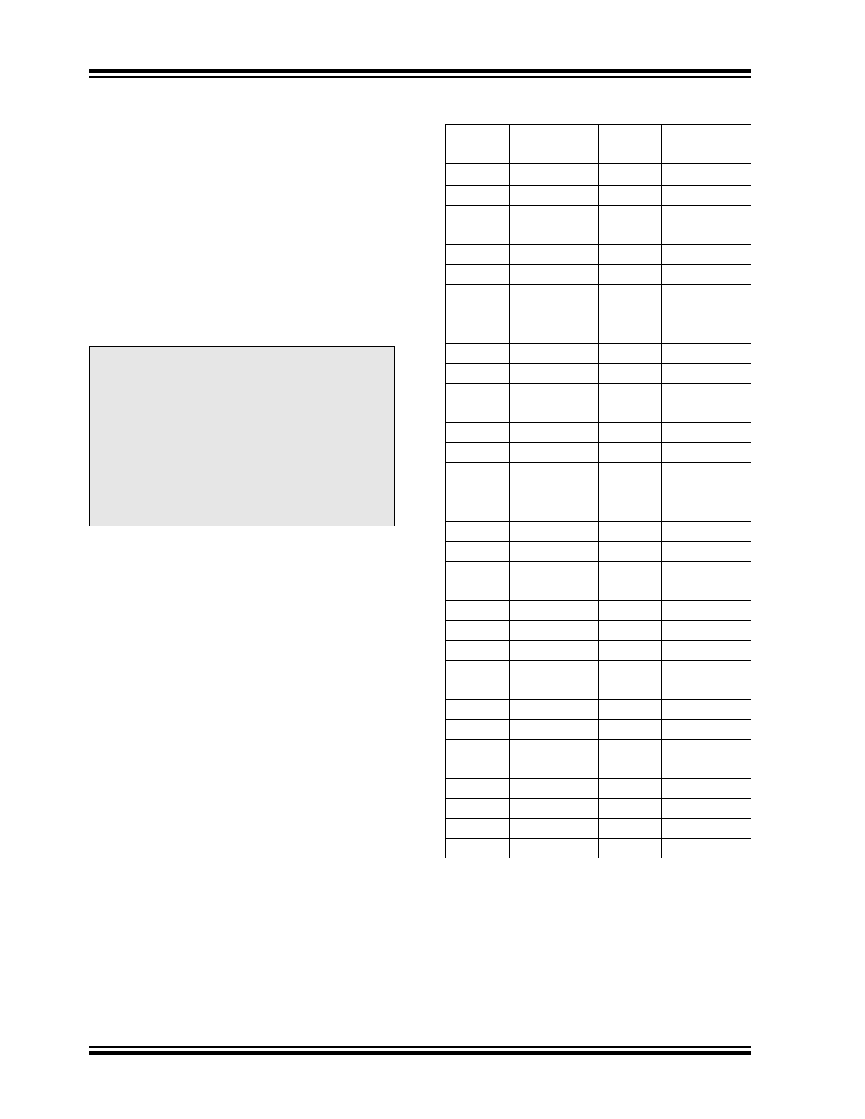
TABLE 2-1:
USER EPROM MEMORY MAP
Note 1: An offset of 0x10 is required to be added
to the addresses shown in the User Pro-
gram Memory Map (Table 2-1) when
programming these locations. There-
fore, there should be 16 Increment
Address commands before program-
ming the contents of the User EPROM
Memory.
2: Do not program outside the specified
user EPROM memory range or
improper operation may occur.
Address
(1)
Location
Name
Address
(1)
Location
Name
00h
IOINTEN
23h
TXID0EID0
01h
IOINTPO
24h
TXID1SIDH
02h
GPLAT
25h
TXID1SIDL
03h
—
(2)
26h
TXID1EID8
04h
OPTREG1
27h
TXID1EID0
05h
T1CON
28h
TXID2SIDH
06h
T2CON
29h
TXID2SIDL
07h
PR1
2Ah
TXID2EID8
08h
PR2
2Bh
TXID2EID0
09h
PWM1DCH
2Ch
ADCMP3H
0Ah
PWM2DCH
2Dh
ADCMP3L
0Bh
CNF1
2Eh
ADCMP2H
0Ch
CNF2
2Fh
ADCMP2L
0Dh
CNF3
30h
ADCMP1H
0Eh
ADCON0
31h
ADCMP1L
0Fh
ADCON1
32h
ADCMP0H
10h
STCON
33h
ADCMP0L
11h
OPTREG2
34h
GPDDR
12h
—
(3)
35h
USER0
13h
—
(3)
36h
USER1
14h
RXMSIDH
37h
USER2
15h
RXMSIDL
38h
USER3
16h
RXMEID8
39h
USER4
17h
RXMEID0
3Ah
USER5
18h
RXF0SIDH
3Bh
USER6
19h
RXF0SIDL
3Ch
USER7
1Ah
RXF0EID8
3Dh
USER8
1Bh
RXF0EID0
3Eh
USER9
1Ch
RXF1SIDH
3Fh
USERA
1Dh
RXF1SIDL
40h
USERB
1Eh
RXF1EID8
41h
USERC
1Fh
RXF1EID0
42h
USERD
20h
TXID0SIDH
43h
USERE
21h
TXID0SIDL
44h
USERF
22h
TXID0EID8
45h
CHKSUM
Note 1: An offset of 0x10 is required.
2: Reserved, Program this location as
0x3FFF.
3: Unimplemented, Program this location as
0x3FFF.

2001 Microchip Technology Inc.
DS20072A-page 3
MCP2505X
3.0
PROGRAMMING MODE ENTRY
A specific hardware sequence is required to force the
device from the normal operating mode into Program-
ming programming mode. After entering into the Pro-
gramming mode, the 2-wire serial interface can be
used to send the commands to the MCP2505X. These
commands are discussed in Section 4.0.
3.1
Programming Entry Sequence
The Programming mode is entered by raising V
DD
.
Then while holding the CLOCK and DATA pins (GP5
and GP4) low, raising the RST pin from V
IL
IHH
Once in this mode, the User EPROM memory and the
configuration memory can be accessed (read and pro-
grammed). The interface is serial and the CLOCK pin
(GP5) is a Schmitt Trigger input in this mode.
The sequence that forces the device into the Program-
ming mode also puts all other logic into the reset state
(the RST pin was initially at V
IL
). This means that all I/
O are in the reset state (High impedance inputs).
Figure 7-2 shows the waveform for entry into Program-
ming mode.
3.2
Programming Operation
The CLOCK pin (GP5) is used as a clock input pin. The
DATA pin (GP4) is used for entering command bits and
data input/output during serial communication.
To input a command, the CLOCK pin (GP5) is cycled
six times. Each command bit is latched on the falling
edge of the clock with the least significant bit (LSb) of
the command being input first. The data on the DATA
pin (GP4) is required to have a minimum setup and
hold time (see Parameter P3 and Parameter P4) with
respect to the falling edge of the clock. Commands that
have data associated with them (read and load) are
specified to have a minimum delay between the com-
mand and the data (Parameter P6).
After this delay, the clock pin is cycled 16 times with the
first cycle being a start bit and the last cycle being a
stop bit. The data is input/output LSb first. During a
read operation the LSb will be transmitted onto the
DATA pin (GP4) on the rising edge of the second cycle,
and during a load operation the LSb will be latched on
the falling edge of the second cycle.
All commands and data words are transmitted LSb first.
The DATA pin value is latched on the falling edge of the
CLOCK pin. A minimum time between the command
and the data word (or another command) is required.
This separation time is shown in Parameter P6 of the
Electrical Specification.
The commands that are available are listed in Table 4-
1. The waveforms for these commands are shown in
Figure 7-3 through Figure 7-8.
Note 1: Do not power any I/O pins before V
DD
is
applied.

MCP2505X
DS20072A-page 4
2001 Microchip Technology Inc.
4.0
PROGRAMMING COMMANDS
There are six commands that the MCP2505X will exe-
cute when in Programming mode. These commands
are shown in Table 4-1. Three of the commands have
data that are required. The Load commands supply
data to the MCP2505X, and the Read command
retrieve data from the MCP2505X.
When the device enters into Programming mode, the
address pointer is pointing to 0x00. The User Program
Memory has an offset of 0x10. So before starting to
program a desired location in the User Program Mem-
ory Map, the Increment Address command must be
executed 16 times.
TABLE 4-1:
PROGRAMMING COMMANDS
4.1
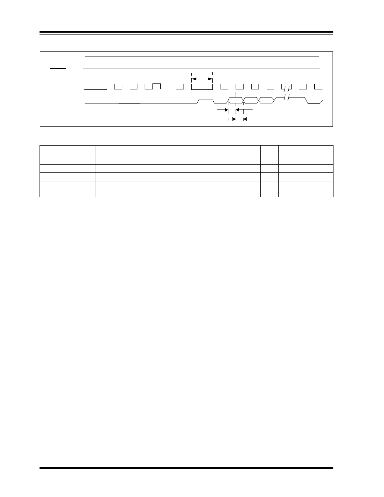
Load Configuration
After receiving this command, the address pointer
points to the Configuration memory space. To address
the MCP250XX Configuration word the Increment
command must be given seven times (see Figure 4-2).
Then by applying 16 clock cycles to the CLOCK pin, a
14-bit “data word” will be loaded into the Transfer Latch
(ready to be programmed into the configuration word,
see Register 5-1). Only the lower 3 bits of the “data
word” should be programmed. The remaining 11 bits of
the “data word” are reserved and should be pro-
grammed as a ‘1’. Programming these bits as a ‘1’ will
ensure that the factory value is not modified. When ver-
ifying this location, only verify against the lower 3 bits
(the bits that were programmed).
After the Load Configuration command is supplied, the
only way to have the address pointer return to pointing
at the User Program Memory is to exit the Program-
ming mode. This is accomplished by taking the voltage
on the RST pin to a low level (V
IL
, Parameter PD8) and
the re-entering into Programming mode (see
Section 3.1).
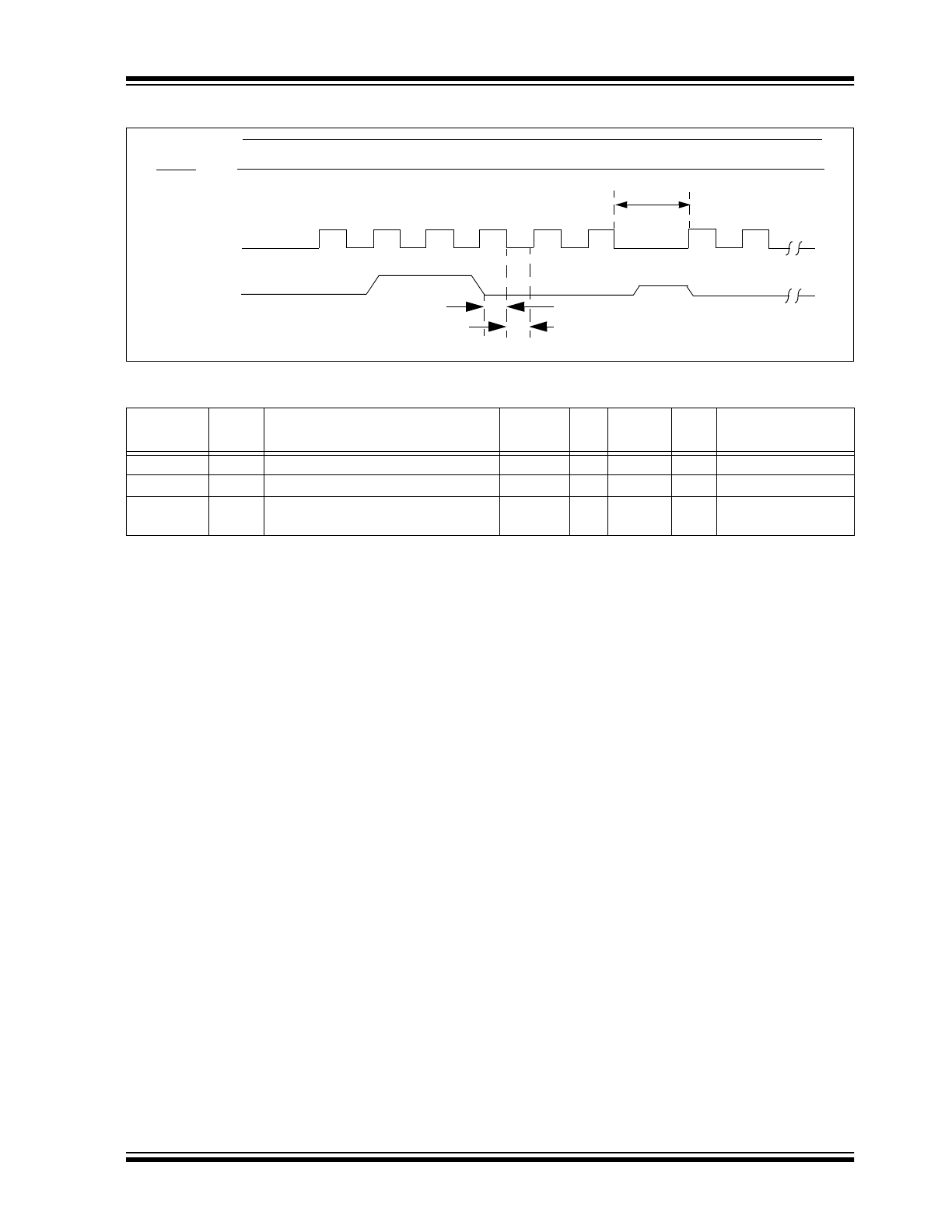
Figure 7-3 shows the waveform for the Load Configu-
ration command and Table 7-3 specifies the timing
parameters that must be meet.
4.2
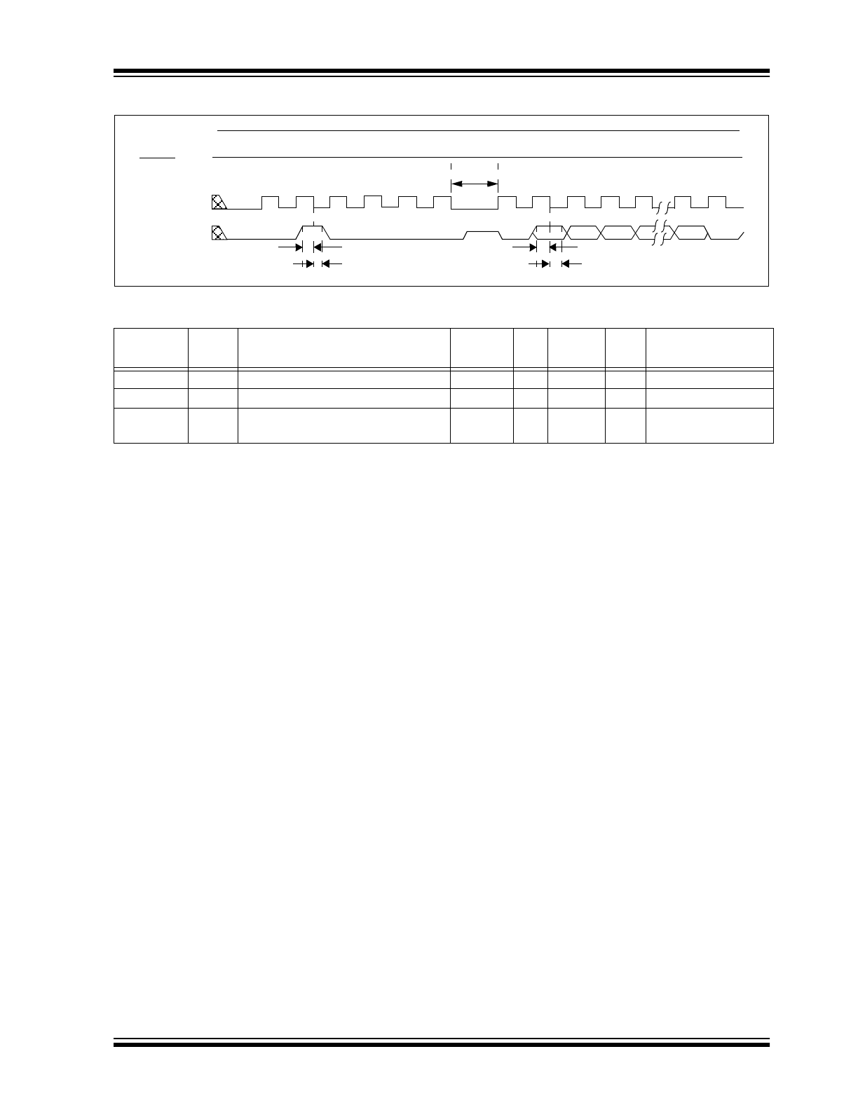
Load Data
After receiving this command, the chip will load in a
14-bit “data word” into the Transfer latch when 16 clock
cycles are applied to the CLOCK pin.
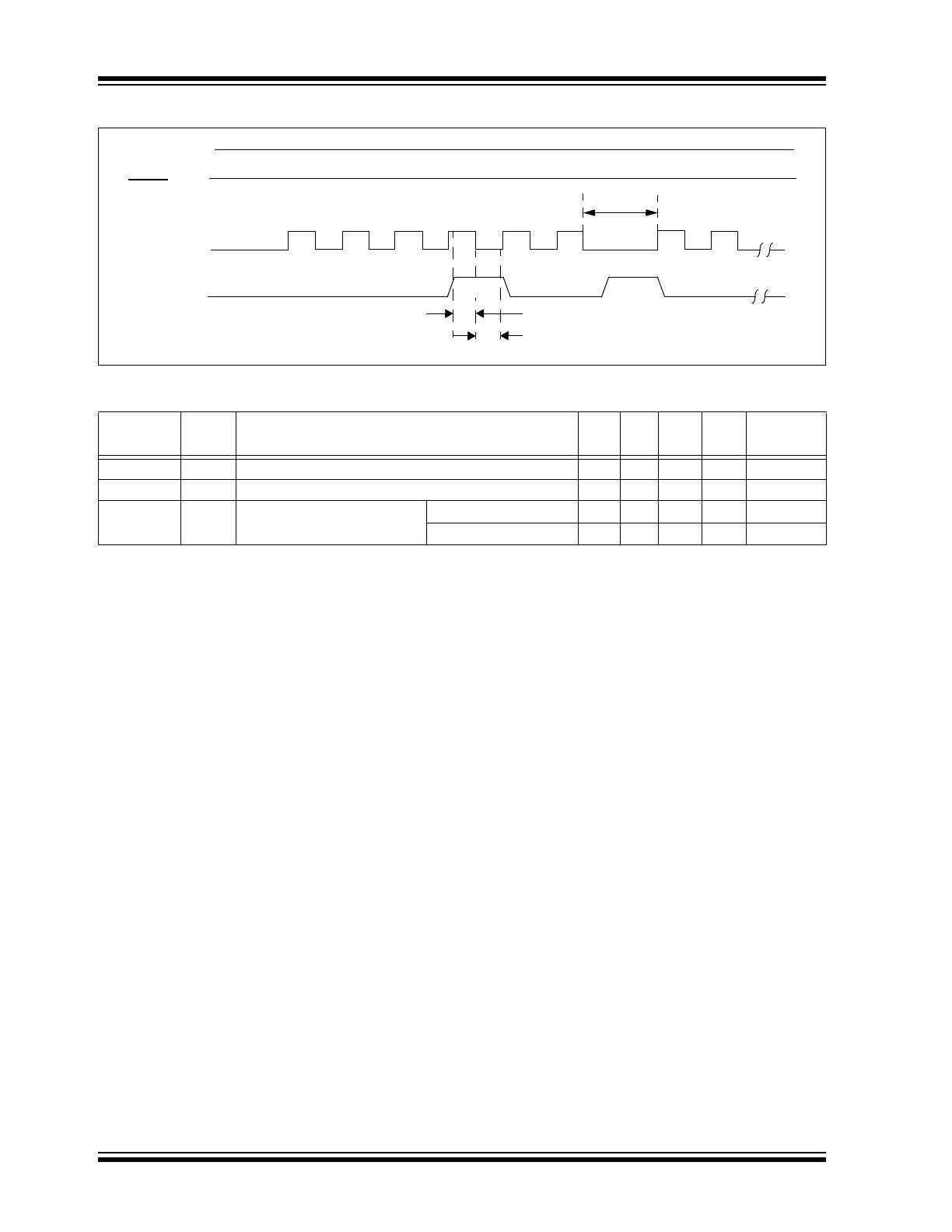
Figure 7-4 shows the waveform for the Load Data com-
mand and Table 7-4 specifies the timing parameters
that must be meet.
4.3
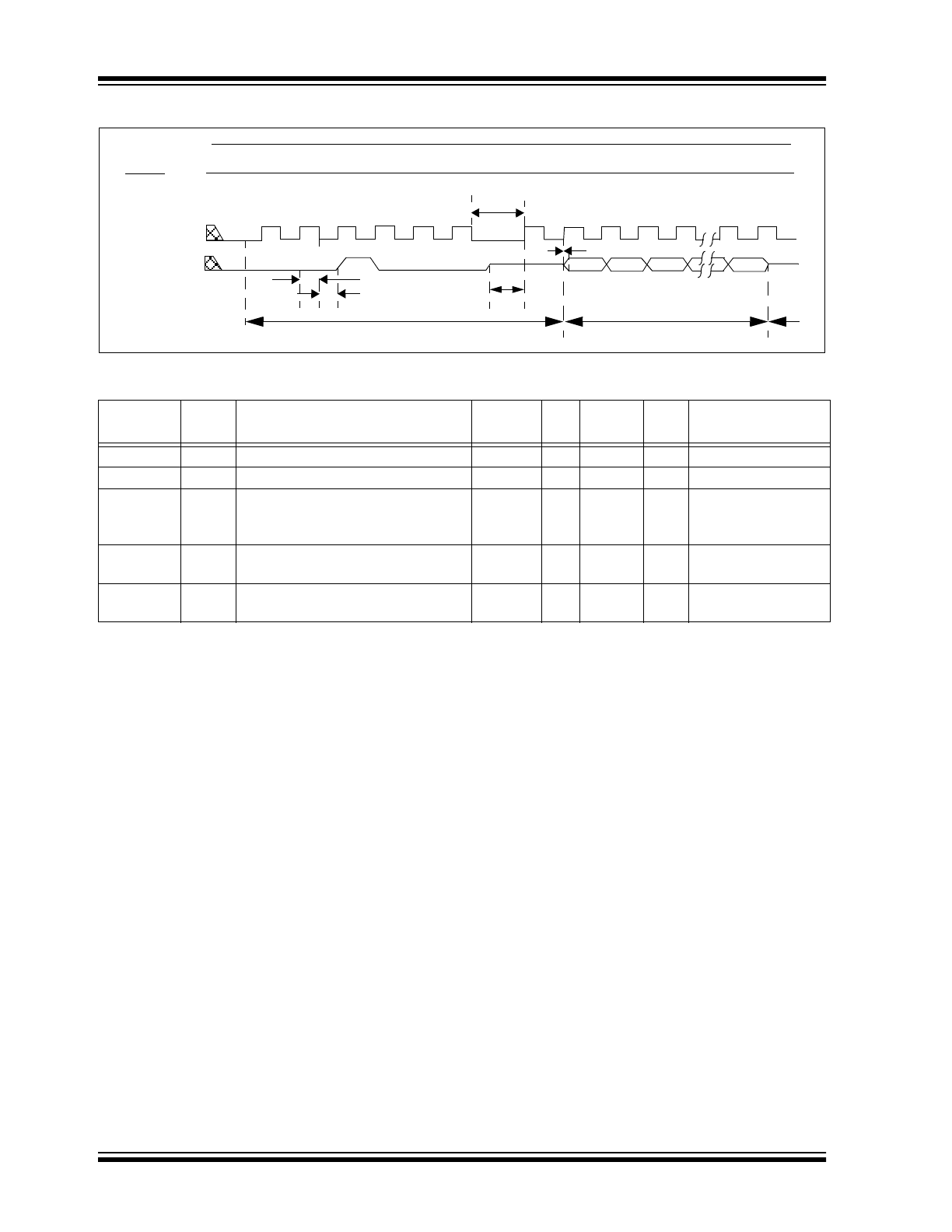
Read Data
After receiving this command (the first 6 bits), the
device data word at the memory address currently
accessed is loaded into the Transfer latch. Then as the
Data is transmitted, the DATA (GP4) pin is automati-
cally configured into an output on the second rising
clock edge, and reverts back to an input (hi-imped-
ance) after the 16th rising edge.
Figure 7-5 shows the waveform for the Read Data
command and Table 7-5 specifies the timing parame-
ters that must be meet.
This command is useful in the verify sequence of the
programming algorithm. This is used to verify that if the
value that was programmed at this location has been
“well programmed”. That is, that the memory cell was
able to retain the value previously written. A memory
verification should be done at the minimum and maxi-
mum voltage that the device will experience within the
application.
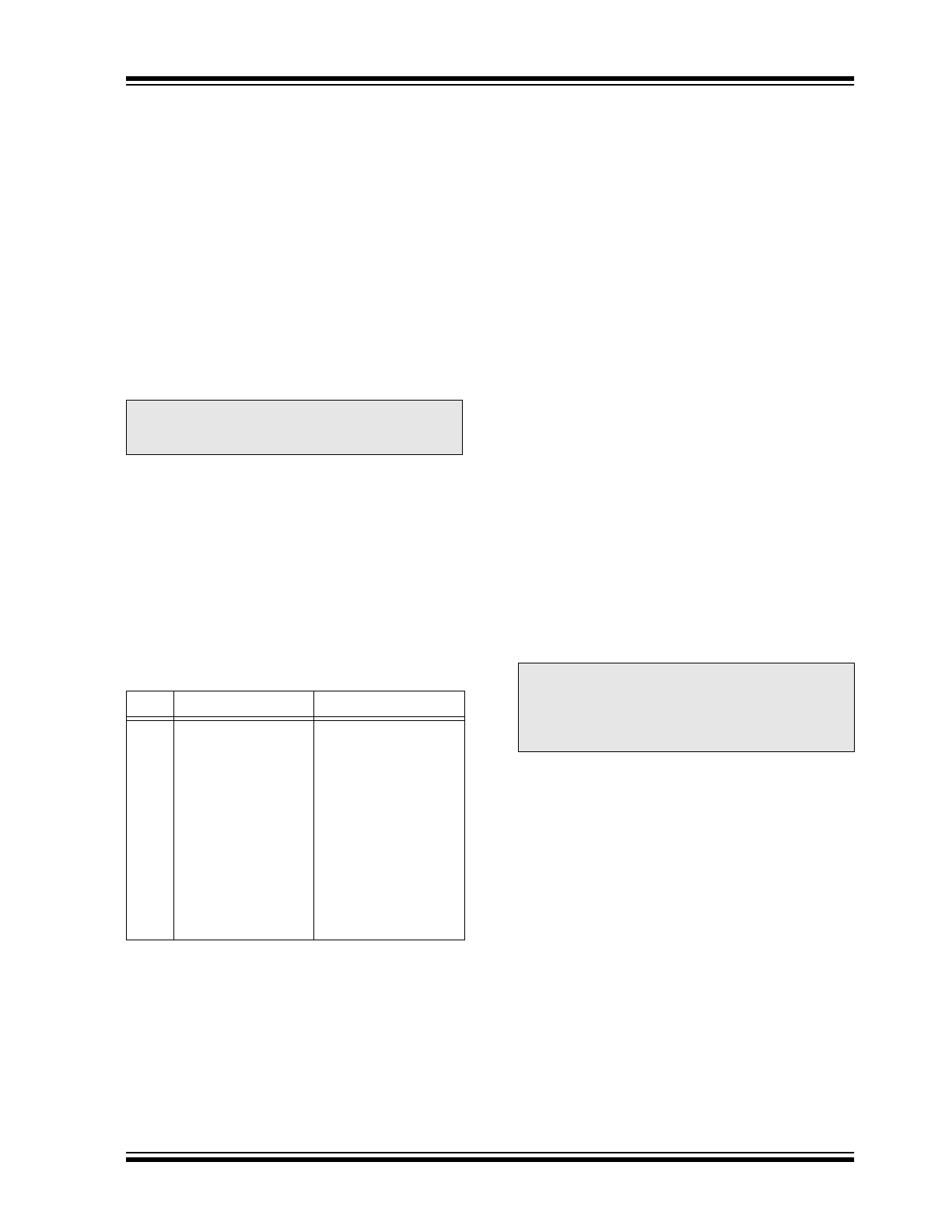
Command
Mapping
(MSb ... LSb)
Data
Load
Configuration
0 0 0 0 0 0 0
, data(14),
0
Load Data
0 0 0 0 1 0 0,1,1,0,1,0,0
,
data(8),
0
Read Data
0 0 0 1 0 0 0
, data(14),
0
Increment
Address
0 0 0 1 1 0
—
Begin
Programming
0 0 1 0 0 0
—
End
Programming
0 0 1 1 1 0
—
2001 Microchip Technology Inc.
DS20072A-page 5
MCP2505X
4.4
Increment Address
The address pointer is incremented when this com-
mand is received.
Figure 7-6 shows the waveform for the Increment
Address command and Table 7-6 specifies the timing
parameters that must be meet.
4.5
Begin Programming
Programming of the appropriate memory (User Pro-
gram Memory or Configuration Memory) will begin after
this command is received and decoded. This program-
ming pulse will continue until an End Programming
command is received. Each programming pulse should
meet a minimum time duration (Parameter P11 in Elec-
trical Specification’s Table 7-7).
Programming should be performed with a series of pro-
gramming pulses (Parameter P11). A programming
pulse is defined as the time between the Begin Pro-
gramming command and the End Programming com-
mand.
Figure 7-7 shows the waveform for the Begin Program-
ming command and Table 7-7 specifies the timing
parameters that must be met.
Example 4-1 shows a typical command sequence that
would be used in the over programming of a device.
EXAMPLE 4-1:
Command Sequence
4.6
End Programming
After receiving this command, the chip stops program-
ming the memory (configuration program memory or
user program memory) that it was programming at the
time.
Figure 7-8 shows the waveform for the End Program-
ming command and Table 7-8 specifies the timing
parameters that must be met.
4.7
Programming Algorithm Requires
Variable V
DD
The algorithm calls for program verification at V
DD
min
as well as V
DD
max. Verification at V
DD
min guarantees
good “erase margin”. Verification at V
DD
max guaran-
tees good “program margin”.
The actual programming must be done with V
DD
in the
V
DDP
range (Parameter PD1).
V
DDP
=
V
DD
range required during programming.
V
DDV
=
V
DD
range required during verification.
V
DDMIN
=
Minimum operating V
DD
specification for
the device.
V
DDMAX
=
Maximum operating V
DD
specification for
the device.
Programmers must verify the MCP2505X at its speci-
fied V
DDMAX
and V
DDMIN
levels. Since Microchip may
introduce future versions of the MCP2505X with a
broader V
DD
range, it is best that these levels are user
selectable (defaults are ok).
Note:
A load command (load configuration or
load data) must be given before every
Begin Programming command.
Step
Command
Comment
1
Load Command
; Data or Configuration
2
Begin Programming
; Pulse #1
; Wait required delay
3
End Programming
4
Load Command
; Data or Configuration
5
Begin Programming
; Pulse #2
; Wait required delay
6
End Programming
:
: ;
Repeat
Load/Begin/
; End Programming
; sequence as needed
Note:
Any programmer not meeting these
requirements may only be classified as
“prototype” or “development” program-
mer but not a “production” quality pro-
grammer.
MCP2505X
DS20072A-page 6
2001 Microchip Technology Inc.
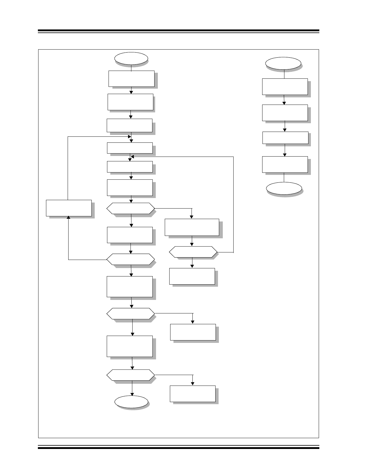
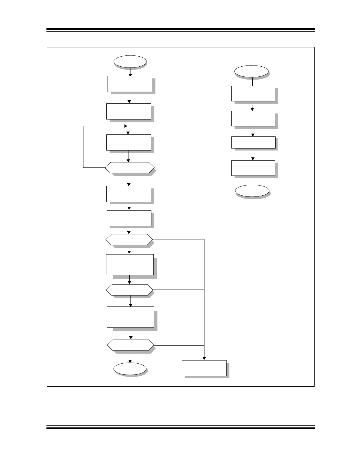
FIGURE 4-1:
PROGRAM FLOW CHART - MCP2505X PROGRAM MEMORY
Start
Set V
DD
= V
DDP
(1)
N = N + 1
Load Data
Command
Increment Address
Command
Report Verify
@ V
DD
MAX
Error
End Programming
Command
Begin Programming
Command
Apply 3N Additional
Program Cycles
Read Data
Command
Program Cycle
N > 25
Data Correct?
Done
No
Yes
Yes
No
No
Yes
Force V
PP
from
Vss to V
IHH
N = 0
All Locations Done?
Verify all Locations
@ V
DD
MIN
.•
V
PP
= V
IHHV
Data Correct?
Yes
Verify all Locations
@ V
DD
MAX
.
V
PP
= V
IHHV
Data Correct?
Yes
Report Programming
Failure
Wait 100
µ
s
Report Verify
@ V
DD
MIN
.
Error
No
No
Note 1:
V
DDP
=
V
DD
range for programming (typically 4.75V - 5.25V).
2:
V
DD
MIN
.
= Minimum
V
DD
for device operation.
V
DD
MAX
.
= Maximum
V
DD
for device operation.
N = # of Program Cycles
Apply 16 Increment
Address Commands
Program Cycle
Return
2001 Microchip Technology Inc.
DS20072A-page 7
MCP2505X
FIGURE 4-2:
PROGRAM FLOW CHART - MCP2505X CONFIGURATION WORD
Start
Load Configuration
Command
Increment Address
Command
Program Cycle
(do 100 times)
Read Data
Command
Report Program
Configuration Error
Data Correct?
Data Correct?
Data Correct?
Incremented 7 times?
Done
Yes
No
No
Yes
No
Yes
Yes
No
Read Data Command
Set V
PP
= V
IHHV
Read Data Command
Set V
PP
= V
IHHV
Force V
PP
from
Vss to V
IHH
Set V
DD
= V
DD
max
Load Data
Command
End Programming
Command
Begin Programming
Command
Wait 100
µ
s
Program Cycle
Return
Set V
DD
= V
DD
min
MCP2505X
DS20072A-page 8
2001 Microchip Technology Inc.
5.0
CONFIGURATION WORD
The MCP2505X family members have several configu-
ration bits. These bits can be programmed (reads ’0’) or
left unprogrammed (reads ’1’) to select various device
configurations. Register 5-1 provides an overview of
configuration bits.
Only the lower 3 bits should be programmed. The
remaining 11 bits are reserved and should be pro-
grammed as a ‘1’. Programming these bits as a ‘1’ will
ensure that the factory value is not modified.
REGISTER 5-1:
CONFIGURATION REGISTER
R-x
R-x
R-x
R-x
R-x
R-x
R-x
R-x
R-x
R-x
R-x
R/P-1
R/P-1
R/P-1
—
—
—
—
—
—
—
—
—
—
—
RSTEN
FOSC1
FOSC0
bit 13
bit 0
bit 13-3 Reserved: Read as ’x’, Program as ‘1’.
bit 2
RSTEN: Reset on GP7 Enable bit
1
= RST function is enabled on the GP7 I/O pin
0
= GP7 is a general purpose I/O pin
bit 1-0
FOSC1:FOSC0: Oscillator Selection bits
11
= RC oscillator
10
= EC (External Clock)
01
= XT oscillator
00
= LP oscillator
Legend:
R = Readable bit
P = Programmable bit
U = Unimplemented bit, read as ‘0’
- n = Value when device is unprogrammed
x = Unknown state
2001 Microchip Technology Inc.
DS20072A-page 9
MCP2505X
6.0
MEMORY VERIFICATION
The User EPROM memory and configuration word is
checksummed. This enhances the validation that the
correct user’s values are programmed into the devices
memory.
6.1 Checksum Calculations
Checksum is calculated by reading the contents of the
MCP2505X User EPROM memory locations and add-
ing the values up. The entire User EPROM memory is
read (00h - 45h). Any carry bits exceeding 16 bits are
ignored. Finally, the configuration word (appropriately
masked) is added to the checksum. Checksum compu-
tation for each member of the MCP2505X devices is
shown in Table 6-1.
The checksum is calculated by summing the following:
• The contents of all User EPROM memory loca-
tions
• The configuration word, appropriately masked
The least significant 16 bits of this sum is the check-
sum.
The Table 6-1 describes how to calculate the check-
sum. When calculating a checksum by reading a
device, the entire User EPROM memory can be read
and summed. The configuration word and ID locations
can always be read.
TABLE 6-1:
CHECKSUM COMPUTATION
Device
Checksum
(1)
Value
Unprogrammed
When:
Addr. 0x000 = 0x25E6
Addr. 0x045 = 0x25E6
MCP2505X
(SUM[0x000:0x045] + (CFGW & 0x07) )
0x7FC1
0x4B8F
Legend: SUM[a:b] = [Sum of locations a through b inclusive]
CFGW = Configuration Word
Note 1:
Checksum
=
[Sum of all the individual expressions] MODULO [0xFFFF]
+ =
Addition
& =
Bitwise
AND
MCP2505X
DS20072A-page 10
2001 Microchip Technology Inc.
7.0
PROGRAM/VERIFY MODE ELECTRICAL CHARACTERISTICS
7.1
DC Characteristics
FIGURE 7-1:
PROGRAMMING DC CHARACTERISTICS WAVEFORMS
TABLE 7-1:
DC CHARACTERISTICS FOR PROGRAMMING MODE (PROGRAM/VERIFY)
Standard Operating Conditions:
Operating Temperature: +10
°
C
≤
T
A
≤
+40
°
C, unless otherwise stated, (25
°
C is recommended)
Operating Voltage: 4.5V
≤
V
DD
≤
5.5V, unless otherwise stated.
Parameter
No.
Sym.
Characteristic
Min.
Typ.
Max.
Units Conditions
PD1 V
DDP
Supply voltage during programming
4.75
5.0
5.25
V
—
PD2
I
DDP
Supply current (from V
DD
)
during programming
—
—
20 mA
—
PD3 V
DDV
Supply voltage during verify
V
DD
min
—
V
DD
max
V
PD4
V
IHH
Voltage on MCLR/V
PP
during
programming/verify
12.75
—
13.25
V
—
PD6
I
PP
Programming supply current
(from V
PP
)
—
—
50
mA —
PD8
V
IL
Voltage input low
level
DATA (GP4)
V
SS
—
0.2 V
DD
V
Schmitt Trigger input
CLOCK (GP5)
V
SS
—
0.2 V
DD
V
Schmitt Trigger input
RESET
V
SS
—
0.2 V
DD
V
—
PD9
V
IH
Voltage input high
level
DATA (GP4)
0.8 V
DD
—
V
DD
V
Schmitt Trigger input
CLOCK (GP5)
0.8 V
DD
—
V
DD
V
Schmitt Trigger input
RESET
0.8 V
DD
—
V
DD
V
—
Note 1: Program must be verified at the minimum and maximum V
DD
limits of the device.
V
DD
V
PP
V
IHHMIN
(PD4)
V
DDMIN
V
IH
(PD9)
V
IL
(PD8)
V
IHHMIN
(PD4)
GP4, GP5
V
IH
V
IL
V
IH
(PD9)
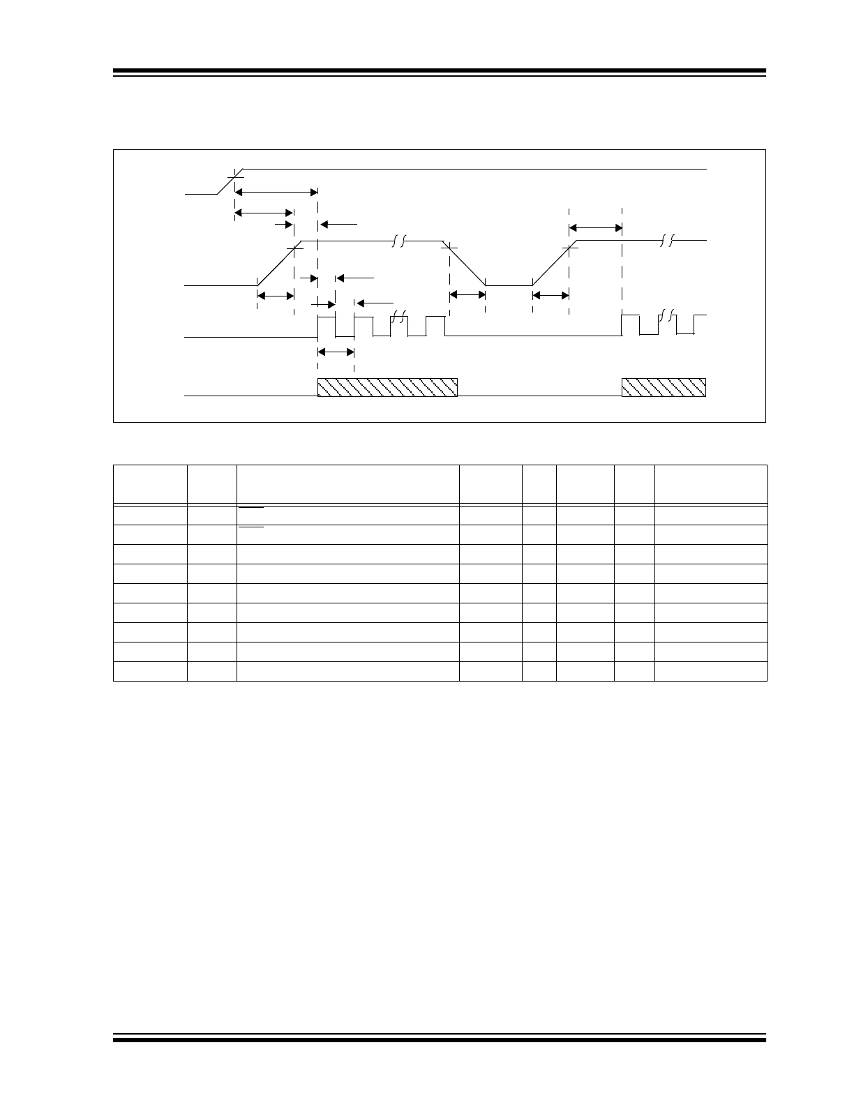
2001 Microchip Technology Inc.
DS20072A-page 11
MCP2505X
7.2
Timing (AC) Characteristics
FIGURE 7-2:
PROGRAMMING MODE ENTRY WAVEFORM
TABLE 7-2:
PROGRAMMING MODE ENTRY TIMING
Parameter
No.
Symbol Characteristic
Min.
Typ.
Max.
Units Conditions
P1
T
R
RST/V
PP
rise time (V
SS
to V
IHH
) 0.15
—
1.0
µ
s
—
P2
T
F
RST Fall time
0.5
—
1.0
µ
s
—
P8
T
HLD
0 Hold time after V
DD
valid to V
PP
= V
IHH
0
—
—
ns
—
P8A
T
PPDP
Hold time after V
PP
= V
IHH
to CLOCK
↑
2
—
—
µ
s
—
P8B
T
HLD
0 Hold time after V
DD
valid to CLOCK
↑
2
—
—
µ
s
—
P9
T
CLOCK
CLOCK pin Period (in Time)
250
—
—
ns
—
P9A
F
CLOCK
CLOCK pin Period (in Frequency)
—
—
4
MHz —
P10A
T
CLK
H CLOCK pin High time
100
—
—
ns
—
P10B
T
CLK
L CLOCK pin Low time
100
—
—
ns
—
Note 1: Program must be verified at the minimum and maximum V
DD
limits of the device.
V
DD
V
PP
V
IHH
V
IH
P1
P8B
CLOCK
P2
P1
P9
P8A
DATA
(GP4)
(GP5)
P8
P10B
P10A
P8A
MCP2505X
DS20072A-page 12
2001 Microchip Technology Inc.
FIGURE 7-3:
LOAD CONFIGURATION COMMAND WAVEFORM
TABLE 7-3:
LOAD CONFIGURATION COMMAND TIMING
Parameter
No.
Symbol Characteristic
Min.
Typ.
Max.
Units Conditions
P3
T
SET
1 Data in setup time before clock
↓
100
—
—
ns
—
P4
T
HLD
1 Data in hold time after clock
↓
100
—
—
ns
—
P6
T
DLY
2 Delay between clock
↓
to clock
↑
of next
command or data
1.0
—
—
µ
s
—
Note 1: Program must be verified at the minimum and maximum V
DD
limits of the device.
P3
P4
0
0
0
P6
0
15
5
4
3
2
1
6
5
0
4
3
0
0
2
1
0
bit 1 bit 2
1
1
CLOCK
DATA
MCLR/V
PP
= V
IHH
V
DD
= V
DDMIN
16
bit 0
2001 Microchip Technology Inc.
DS20072A-page 13
MCP2505X
FIGURE 7-4:
LOAD DATA COMMAND WAVEFORM
TABLE 7-4:
LOAD DATA COMMAND TIMING
Parameter
No.
Symbol Characteristic
Min.
Typ.
Max.
Units Conditions
P3
T
SET
1 Data in setup time before clock
↓
100
—
—
ns
—
P4
T
HLD
1 Data in hold time after clock
↓
100
—
—
ns
—
P6
T
DLY
2 Delay between clock
↓
to clock
↑
of
next command or data
1.0
—
—
µ
s
—
Note 1: Program must be verified at the minimum and maximum V
DD
limits of the device.
0
0
0
P6
0
15
5
4
3
2
1
6
5
0
4
3
0
1
2
1
0
CLOCK
DATA
MCLR/V
PP
= V
IHH
V
DD
= V
DDMIN
P3
P4
P3
P4
16
MCP2505X
DS20072A-page 14
2001 Microchip Technology Inc.
FIGURE 7-5:
READ DATA COMMAND WAVEFORM
TABLE 7-5:
READ DATA COMMAND TIMING
Parameter
No.
Symbol Characteristic
Min.
Typ.
Max.
Units Conditions
P3
T
SET
1 Data in setup time before clock
↓
100
—
—
ns
—
P4
T
HLD
1 Data in hold time after clock
↓
100
—
—
ns
—
P5
T
DLY
1 Data input not driven to next clock
input (delay required between com-
mand/data or command/command)
0.9
—
—
µ
s
—
P6
T
DLY
2 Delay between clock
↓
to clock
↑
of
next command or data
1.0
—
—
µ
s
—
P7
T
DLY
3 Clock
↑
to data out valid
(during read data)
—
—
200
ns
—
Note 1: Program must be verified at the minimum and maximum V
DD
limits of the device.
0
0
P5
P6
15
5
4
3
2
1
6
5
0
4
3
0
1
2
1
CLOCK
DATA
0
DATA line is input to device
DATA line is output
P7
MCLR/V
PP
= V
IHH
V
DD
= V
DDMIN
from device
16
P4
P3
2001 Microchip Technology Inc.
DS20072A-page 15
MCP2505X
FIGURE 7-6:
INCREMENT ADDRESS COMMAND WAVEFORM
TABLE 7-6:
INCREMENT ADDRESS TIMING
Parameter
No.
Symbol Characteristic
Min.
Typ.
Max.
Units Conditions
P3
T
SET
1 Data in setup time before clock
↓
100
—
—
ns
—
P4
T
HLD
1 Data in hold time after clock
↓
100
—
—
ns
—
P6
T
DLY
2 Delay between clock
↓
to clock
↑
of
next command or data
1.0
—
—
µ
s
—
Note 1: Program must be verified at the minimum and maximum V
DD
limits of the device.
0
0
0
0
0
0
1
1
1
2
3
4
5
6
1
2
P3
P4
P6
Next Command
CLOCK
DATA
MCLR/V
PP
= V
IHH
V
DD
= V
DDMIN
MCP2505X
DS20072A-page 16
2001 Microchip Technology Inc.
FIGURE 7-7:
BEGIN PROGRAMMING COMMAND WAVEFORM
TABLE 7-7:
BEGIN PROGRAMMING COMMAND TIMING
Parameter
No.
Symbol Characteristic
Min. Typ. Max. Units Conditions
P3
T
SET
1 Data in setup time before clock
↓
100
—
—
ns
—
P4
T
HLD
1 Data in hold time after clock
↓
100
—
—
ns
—
P11
Programming Pulse Width
User Memory
90
100
110
µ
s
—
Configuration Memory
90
100
110
µ
s
—
Note 1: Program must be verified at the minimum and maximum V
DD
limits of the device.
0
1
0
0
0
0
0
0
1
2
3
4
5
6
1
2
P11
End Programming
CLOCK
DATA
MCLR/V
PP
= V
IHH
V
DD
= V
DDMIN
Command
P3
P4
2001 Microchip Technology Inc.
DS20072A-page 17
MCP2505X
FIGURE 7-8:
END PROGRAMMING COMMAND WAVEFORM
TABLE 7-8:
END PROGRAMMING COMMAND TIMING
Parameter
No.
Symbol Characteristic
Min. Typ. Max. Units Conditions
P3
T
SET
1 Data in setup time before clock
↓
100
—
—
ns
—
P4
T
HLD
1 Data in hold time after clock
↓
100
—
—
ns
—
P6
T
DLY
2 Delay between clock
↓
to clock
↑
of next command or
data
1.0
—
—
µ
s
—
P11
Programming Pulse Width
(1)
User
Memory
90
100
110
µ
s
—
Configuration Memory
90
100
110
µ
s
—
Note 1: Only required if the previous command was the Begin Programming Command.
2: Program must be verified at the minimum and maximum V
DD
limits of the device.
0
1
0
0
0
0
1
1
1
2
3
4
5
6
1
2
P6
Next Command
CLOCK
DATA
MCLR/V
PP
= V
IHH
V
DD
= V
DDMIN
P11
P3
P4

MCP2505X
DS20072A-page 18
2001 Microchip Technology Inc.
NOTES:
2001 Microchip Technology Inc.
DS20072A-page 19
MCP2505X
“All rights reserved. Copyright © 2001, Microchip
Technology Incorporated, USA. Information contained
in this publication regarding device applications and the
like is intended through suggestion only and may be
superseded by updates. No representation or warranty
is given and no liability is assumed by Microchip
Technology Incorporated with respect to the accuracy
or use of such information, or infringement of patents or
other intellectual property rights arising from such use
or otherwise. Use of Microchip’s products as critical
components in life support systems is not authorized
except with express written approval by Microchip. No
licenses are conveyed, implicitly or otherwise, under
any intellectual property rights. The Microchip logo and
name are registered trademarks of Microchip
Technology Inc. in the U.S.A. and other countries. All
rights reserved. All other trademarks mentioned herein
are the property of their respective companies. No
licenses are conveyed, implicitly or otherwise, under
any intellectual property rights.”
Trademarks
The Microchip name, logo, PIC, PICmicro,
PICMASTER, PICSTART, PRO MATE, K
EE
L
OQ
,
SEEVAL, MPLAB and The Embedded Control
Solutions Company are registered trademarks of
Microchip Technology Incorporated in the U.S.A. and
other countries.
Total Endurance, ICSP, In-Circuit Serial Programming,
FilterLab, MXDEV, microID, FlexROM, fuzzyLAB,
MPASM, MPLINK, MPLIB, PICDEM, ICEPIC,
Migratable Memory, FanSense, ECONOMONITOR,
SelectMode and microPort are trademarks of
Microchip Technology Incorporated in the U.S.A.
Serialized Quick Term Programming (SQTP) is a
service mark of Microchip Technology Incorporated in
the U.S.A.
All other trademarks mentioned herein are property of
their respective companies.
© 2001, Microchip Technology Incorporated, Printed in
the U.S.A., All Rights Reserved.
Microchip received QS-9000 quality system
certification for its worldwide headquarters,
design and wafer fabrication facilities in
Chandler and Tempe, Arizona in July 1999. The
Company’s quality system processes and
procedures are QS-9000 compliant for its
PICmicro
®
8-bit MCUs, K
EE
L
OQ
®
code hopping
devices, Serial EEPROMs and microperipheral
products. In addition, Microchip’s quality
system for the design and manufacture of
development systems is ISO 9001 certified.

Information contained in this publication regarding device applications and the like is intended through suggestion only and may be superseded by
updates. It is your responsibility to ensure that your application meets with your specifications. No representation or warranty is given and no liability is
assumed by Microchip Technology Incorporated with respect to the accuracy or use of such information, or infringement of patents or other intellectual
property rights arising from such use or otherwise. Use of Microchip’s products as critical components in life support systems is not authorized except with
express written approval by Microchip. No licenses are conveyed, implicitly or otherwise, except as maybe explicitly expressed herein, under any intellec-
tual property rights. The Microchip logo and name are registered trademarks of Microchip Technology Inc. in the U.S.A. and other countries. All rights
reserved. All other trademarks mentioned herein are the property of their respective companies.
DS20072A-page 20
2001 Microchip Technology Inc.
All rights reserved. © 2001 Microchip Technology Incorporated. Printed in the USA. 3/01
Printed on recycled paper.
M
AMERICAS
Corporate Office
2355 West Chandler Blvd.
Chandler, AZ 85224-6199
Tel: 480-792-7200 Fax: 480-792-7277
Technical Support: 480-792-7627
Web Address: http://www.microchip.com
Rocky Mountain
2355 West Chandler Blvd.
Chandler, AZ 85224-6199
Tel: 480-792-7966 Fax: 480-792-7456
Atlanta
500 Sugar Mill Road, Suite 200B
Atlanta, GA 30350
Tel: 770-640-0034 Fax: 770-640-0307
Austin
Analog Product Sales
8303 MoPac Expressway North
Suite A-201
Austin, TX 78759
Tel: 512-345-2030 Fax: 512-345-6085
Boston
2 Lan Drive, Suite 120
Westford, MA 01886
Tel: 978-692-3848 Fax: 978-692-3821
Boston
Analog Product Sales
Unit A-8-1 Millbrook Tarry Condominium
97 Lowell Road
Concord, MA 01742
Tel: 978-371-6400 Fax: 978-371-0050
Chicago
333 Pierce Road, Suite 180
Itasca, IL 60143
Tel: 630-285-0071 Fax: 630-285-0075
Dallas
4570 Westgrove Drive, Suite 160
Addison, TX 75001
Tel: 972-818-7423 Fax: 972-818-2924
Dayton
Two Prestige Place, Suite 130
Miamisburg, OH 45342
Tel: 937-291-1654 Fax: 937-291-9175
Detroit
Tri-Atria Office Building
32255 Northwestern Highway, Suite 190
Farmington Hills, MI 48334
Tel: 248-538-2250 Fax: 248-538-2260
Los Angeles
18201 Von Karman, Suite 1090
Irvine, CA 92612
Tel: 949-263-1888 Fax: 949-263-1338
Mountain View
Analog Product Sales
1300 Terra Bella Avenue
Mountain View, CA 94043-1836
Tel: 650-968-9241 Fax: 650-967-1590
New York
150 Motor Parkway, Suite 202
Hauppauge, NY 11788
Tel: 631-273-5305 Fax: 631-273-5335
San Jose
Microchip Technology Inc.
2107 North First Street, Suite 590
San Jose, CA 95131
Tel: 408-436-7950 Fax: 408-436-7955
Toronto
6285 Northam Drive, Suite 108
Mississauga, Ontario L4V 1X5, Canada
Tel: 905-673-0699 Fax: 905-673-6509
ASIA/PACIFIC
Australia
Microchip Technology Australia Pty Ltd
Suite 22, 41 Rawson Street
Epping 2121, NSW
Australia
Tel: 61-2-9868-6733 Fax: 61-2-9868-6755
China - Beijing
Microchip Technology Beijing Office
Unit 915
New China Hong Kong Manhattan Bldg.
No. 6 Chaoyangmen Beidajie
Beijing, 100027, No. China
Tel: 86-10-85282100 Fax: 86-10-85282104
China - Shanghai
Microchip Technology Shanghai Office
Room 701, Bldg. B
Far East International Plaza
No. 317 Xian Xia Road
Shanghai, 200051
Tel: 86-21-6275-5700 Fax: 86-21-6275-5060
Hong Kong
Microchip Asia Pacific
RM 2101, Tower 2, Metroplaza
223 Hing Fong Road
Kwai Fong, N.T., Hong Kong
Tel: 852-2401-1200 Fax: 852-2401-3431
India
Microchip Technology Inc.
India Liaison Office
Divyasree Chambers
1 Floor, Wing A (A3/A4)
No. 11, O’Shaugnessey Road
Bangalore, 560 025, India
Tel: 91-80-2290061 Fax: 91-80-2290062
Japan
Microchip Technology Intl. Inc.
Benex S-1 6F
3-18-20, Shinyokohama
Kohoku-Ku, Yokohama-shi
Kanagawa, 222-0033, Japan
Tel: 81-45-471- 6166 Fax: 81-45-471-6122
ASIA/PACIFIC
(continued)
Korea
Microchip Technology Korea
168-1, Youngbo Bldg. 3 Floor
Samsung-Dong, Kangnam-Ku
Seoul, Korea
Tel: 82-2-554-7200 Fax: 82-2-558-5934
Singapore
Microchip Technology Singapore Pte Ltd.
200 Middle Road
#07-02 Prime Centre
Singapore, 188980
Tel: 65-334-8870 Fax: 65-334-8850
Taiwan
Microchip Technology Taiwan
11F-3, No. 207
Tung Hua North Road
Taipei, 105, Taiwan
Tel: 886-2-2717-7175 Fax: 886-2-2545-0139
EUROPE
Denmark
Microchip Technology Denmark ApS
Regus Business Centre
Lautrup hoj 1-3
Ballerup DK-2750 Denmark
Tel: 45 4420 9895 Fax: 45 4420 9910
France
Arizona Microchip Technology SARL
Parc d’Activite du Moulin de Massy
43 Rue du Saule Trapu
Batiment A - ler Etage
91300 Massy, France
Tel: 33-1-69-53-63-20 Fax: 33-1-69-30-90-79
Germany
Arizona Microchip Technology GmbH
Gustav-Heinemann Ring 125
D-81739 Munich, Germany
Tel: 49-89-627-144 0 Fax: 49-89-627-144-44
Germany
Analog Product Sales
Lochhamer Strasse 13
D-82152 Martinsried, Germany
Tel: 49-89-895650-0 Fax: 49-89-895650-22
Italy
Arizona Microchip Technology SRL
Centro Direzionale Colleoni
Palazzo Taurus 1 V. Le Colleoni 1
20041 Agrate Brianza
Milan, Italy
Tel: 39-039-65791-1 Fax: 39-039-6899883
United Kingdom
Arizona Microchip Technology Ltd.
505 Eskdale Road
Winnersh Triangle
Wokingham
Berkshire, England RG41 5TU
Tel: 44 118 921 5869 Fax: 44-118 921-5820
01/30/01
W
ORLDWIDE
S
ALES
AND
S
ERVICE