
2007-2017 Microchip Technology Inc.
DS20001664E-page 1
MCP2502X/5X
Features
• Implements CAN V2.0B
- Programmable bit rate up to 1 Mb/s
- One programmable mask
- Two programmable filters
- Three auto-transmit buffers
- Two message reception buffers
- Does not require synchronization or
configuration messages
• Hardware Features
- Non-volatile memory for user configuration
- User configuration automatically loaded on
Power-up
- Eight general-purpose I/O lines individually
selectable as inputs or outputs
- Individually selectable transmit-on-pin-
change for each input
- Four 10-bit, analog input channels with
programmable conversion clock and V
REF
sources (MCP2505X devices only)
- Message scheduling capability
- Two 10-bit PWM outputs with independently
programmable frequencies
- Device configuration can be modified via
CAN bus messages
- In-Circuit Serial Programming™ (ICSP™) of
default Configuration memory
- Optional 1-wire CAN bus operation
• Low-power CMOS technology
- Operates from 2.7V to 5.5V
- 10 mA active current, typical
- 30 µA standby current (CAN Sleep mode)
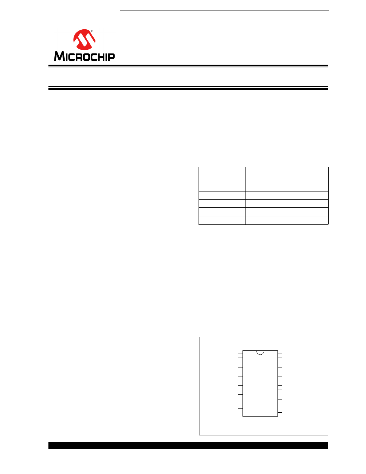
• 14-pin PDIP (300 mil) and SOIC (150 mil)
packages
• Available temperature ranges:
- Industrial (I): -40°C to +85°C
- Extended (E): -40°C to +125°C
Description
The MCP2502X/5X devices operate as I/O expanders
for a Controller Area Network (CAN) system,
supporting CAN v2.0B active, with bus rates up to
1 Mb/s. The MCP2502X/5X allows a simple CAN node
to be implemented without the need for a
microcontroller.
The devices are identical, with the following
exceptions:
The MCP2502X/5X devices feature a number of
peripherals, including digital I/Os, four-channel 10-bit
A/D (MCP2505X), and PWM outputs with automatic
message transmission on change-of-input state. This
includes an analog input exceeding a preset threshold.
One mask and two acceptance filters are provided to
give maximum flexibility during system design with
respect to identifiers that the device will respond to.
The device can also be configured to automatically
transmit a unique message whenever any of several
error conditions occur.
The device is pre-programmed in non-volatile memory
so that the part defaults to a specific configuration at
Power-up.
Package Types
Device
A/D
One Wire
Digital
CANbus
MCP25020
No
No
MCP25025
No
Yes
MCP25050
Yes
No
MCP25055
Yes
Yes
GP0/AN0
GP1/AN1
V
DD
TXCAN/TXRXCAN*
RXCAN/NC*
GP5/V
REF
+
1
2
3
4
GP4/V
REF
-
GP6/CLKOUT
14
13
12
11
10
GP3/AN3/PWM2
OSC1/CLKIN
GP2/AN2/PWM1
5
6
7
8
9
OSC2
V
SS
GP7/RST/V
PP
PDIP/SOIC
* One-wire option available on MCP250X5 devices.
CAN I/O Expander Family
Not Recommended for New Designs
Use MCP2515 or MCP25625

MCP2502X/5X
DS20001664E-page 2
2007-2017 Microchip Technology Inc.
Definition of Terms
The following terms are used throughout this
document:
I/O Expander – refers to the integrated circuit (IC)
device being described (MCP2502X/5X).
Input Message – term given to messages that are
received by the MCP2502X/5X and cause the internal
registers to be modified. Once the register modification
has been performed, the MCP2502X/5X transmits a
Command Acknowledge message to indicate that the
command was received and processed.
Command Acknowledge Message – term given to
the message that is automatically transmitted by the
MCP2502X/5X after receiving and processing an input
message.
Information Request Message – term given to the
Remote Request messages that are received by the
MCP2502X/5X that subsequently generate an output
message (data frame) in response.
Output Message – term given to the message that the
MCP2502X/5X sends in response to an Information
Request message.
On Bus Message – term given to the message that the
MCP2502X/5X transmits after completing the Power-On
and/or Self-Configuration sequences at timed intervals,
if enabled.
Self-Configuration – term used to describe the
process of transferring the contents of the EPROM
memory array to the SRAM memory array.
On Bus – term used to describe the condition when the
MCP2502X/5X is fully-configured and ready to transmit
or receive on the bus. This is the only state in which the
MCP2502X/5X can transmit on the bus.
Edge Detection – refers to the MCP2502X/5X’s ability
to automatically transmit a message based on the
occurrence of a predefined edge on any digital input.
Threshold Detection – refers to the MCP2502X/5X’s
ability to automatically transmit a message when a
predefined analog threshold is reached.
2007-2017 Microchip Technology Inc.
DS20001664E-page 3
MCP2502X/5X
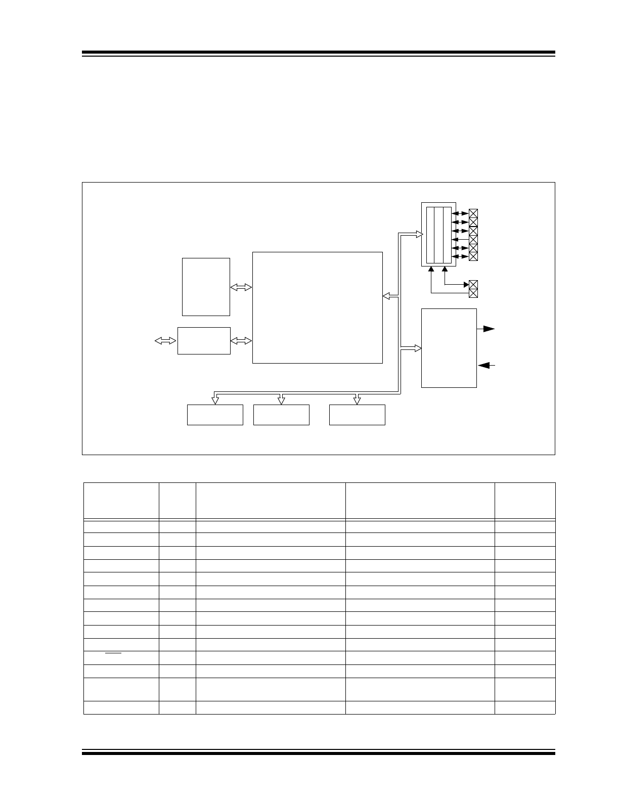
1.0
DEVICE OVERVIEW
This document contains device-specific information on
the MCP2502X/5X family of CAN I/O expanders. The
CAN protocol is not discussed in depth in this docu-
ment. Additional information on the CAN protocol can
be found in the CAN specification, as defined by Rob-
ert Bosch GmbH.
Figure 1-1
is the block diagram of the MCP2502X/5X
and
Table 1-1
is the pinout description.
FIGURE 1-1:
MCP2502X/5X BLOCK DIAGRAM
TABLE 1-1:
PINOUT DESCRIPTION
GPIO
GP4/V
REF
-
GP3/AN3/PWM2
GP2/AN2/PWM1
GP1/AN1
GP0/AN0
GP5/V
REF
+
GP6/CLKOUT
GP7RST/V
PP
User
Timing
Generation
OSC1/CLKIN
OSC2/CLKOUT
CAN
Protocol
Engine
RXCAN
TXCAN/
A/D
PWM1
PWM2
Memory
*
TXRXCAN
* Only the MCP2505X devices have the A/D module.
State Machine
and
Control Logic
Pin
Name
Pin
Number
Standard Function
Alternate Function
Programming
Mode
Function
GP0/AN0
*
1
Bidirectional I/O pin, TTL input buffer
Analog input channel
None
GP1/AN1
*
2
Bidirectional I/O pin, TTL input buffer
Analog input channel
None
GP2/AN2/PWM2
*
3
Bidirectional I/O pin, TTL input buffer
Analog input/PWM output
None
GP3/AN3/PWM3
*
4
Bidirectional I/O pin, TTL input buffer
Analog input/PWM output
None
GP4/V
REF
-
5
Bidirectional I/O pin, TTL input buffer
External V
REF
-
Data
GP5/V
REF
+
6
Bidirectional I/O pin, TTL input buffer
External V
REF
+ input
Clock
V
SS
7
Ground
None
Ground
OSC1/CLKIN
8
External oscillator input
External clock input
None
OSC2
9
External oscillator output
None
None
GP6/CLKOUT
10
Bidirectional I/O pin, TTL input buffer
CLKOUT output
None
GP7/RST/V
PP
11
Input pin, TTL input buffer
External Reset input
V
PP
RXCAN
12
CAN data receive input
Not connected for 1-wire operation
None
TXCAN/TXRXCAN
13
CAN data transmit output
CAN TX and RX for 1-wire operation
(MCP250X5)
None
V
DD
14
Power
None
Power
* Only the MCP2505X devices have the A/D module.

MCP2502X/5X
DS20001664E-page 4
2007-2017 Microchip Technology Inc.
NOTES:
2007-2017 Microchip Technology Inc.
DS20001664E-page 5
MCP2502X/5X
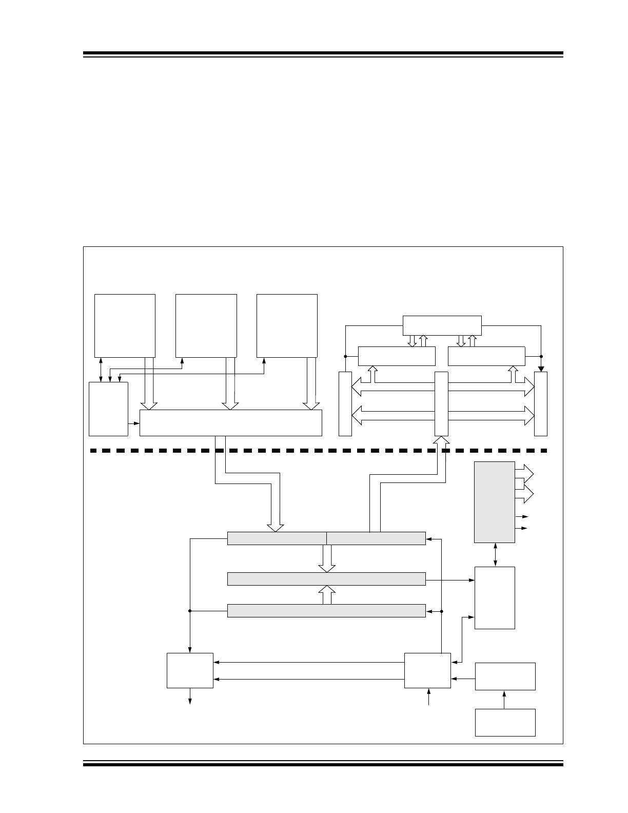
2.0
CAN MODULE
The CAN module is a protocol controller that converts
between raw digital data and CAN message packets.
The main functional block of the CAN module is shown
in
Figure 2-1
and consists of:
• CAN protocol engine
• Buffers, masks and filters
The module features include:
• Implementation of the CAN protocol
• Double-buffered receiver with two separate
receive buffers
• One full-acceptance mask (standard and
extended)
• Two full-acceptance filters (standard and
extended)
• One filter for each receive buffer
• Three prioritized transmit buffers for transmitting
predefined message types
• Automatic wake-up on bus traffic function
• Error management logic for transmit and receive
error states
• Low-power SLEEP mode
FIGURE 2-1:
CAN MODULE
R
X
B
0
Acceptance Filter
RXF1
R
X
B
1
Identifier
Data Field
Data Field
Identifier
M
A
B
Acceptance Mask
RXM
Acceptance Filter
RXF0
TXREQ
TXB2
ABTF MLOA TXERR
ME
SSAGE
Message
Queue
Control
Transmit Byte Sequencer
TXREQ
TXB0
ABTF MLOA TXERR
ME
SSAGE
CRC<14:0>
Comparator
Receive<7:0>
Transmit<7:0>
Receive
Error
Transmit
Error
Protocol
REC
TEC
ErrPas
BusOff
Finite
State
Machine
Counter
Counter
Shift<14:0>
{Transmit<5:0>, Receive<8:0>}
Transmit
Logic
Bit
Timing
Logic
TXCAN/TXRXCAN
RXCAN
Configuration
Registers
Clock
Generator
PROTOCOL
ENGINE
BUFFERS
TXREQ
TXB1
ABTF MLOA TXERR
ME
SSAGE
A
C
C
E
P
T
A
C
C
E
P
T
MCP2502X/5X
DS20001664E-page 6
2007-2017 Microchip Technology Inc.
2.1
CAN Protocol Finite State Machine
The heart of the engine is the Finite State Machine
(FSM). This state machine sequences through mes-
sages on a bit-by-bit basis, changing states as the
fields of the various frame types are transmitted or
received. The FSM is a sequencer controlling the
sequential data stream between the TX/RX Shift
register, the CRC register and the bus line. The FSM
also controls the Error Management Logic (EML) and
the parallel data stream between the TX/RX Shift reg-
isters and the buffers. The FSM ensures that the pro-
cesses of reception, arbitration, transmission and error
signaling are performed according to the CAN protocol.
The automatic retransmission of messages on the bus
line is also handled.
2.2
Cyclic Redundancy Check (CRC)
The CRC register generates the CRC code that is
transmitted after either the Control field (for messages
with 0 data bytes) or the Data field, and is used to check
the CRC field of incoming messages.
2.3
Error Management Logic
The error management logic is responsible for the fault
confinement of the CAN device. Its two counters, the
Receive Error Counter (REC) and the Transmit Error
Counter (TEC), are incremented and decremented by
commands from the bit stream processor. According to
the values of the error counters, the MCP2502X/5X is
set into one the following states: Error-Active,
Error-Passive, or Bus-Off.
Error-Active: both error counters are below the error-
passive limit of 128.
Error-Passive: at least one of the error counters (TEC
or REC) equals or exceeds 128.
Bus-Off: the transmit error counter (TEC) equals or
exceeds the bus-off limit of 256. The device remains in
this state until the bus-off recovery sequence is
received. The bus-off recovery sequence consists of
128 occurrences of 11 consecutive recessive bits.
FIGURE 2-2:
ERROR MODES STATE DIAGRAM
Note:
The MCP2502X/5X, after going bus-off,
will recover to error-active automatically if
the bus remains idle for 128 x 11 bits.
OPTREG2.ERRE must be set to force the
MCP2502X/5X to enter Listen-Only
mode, instead of Normal mode, during
bus recovery. The current error mode
(except for bus-off) of the MCP2502X/5X
can be determined by reading the EFLG
register via the Read CAN error message.
Bus-Off
Error-Active
Error-Passive
REC < 127 or
TEC < 127
REC > 127 or
TEC > 127
TEC > 255
RESET
128 occurrences of
11 consecutive
“recessive” bits

2007-2017 Microchip Technology Inc.
DS20001664E-page 7
MCP2502X/5X
REGISTER 2-1:
TEC - TRANSMITTER ERROR COUNTER
REGISTER 2-2:
REC - RECEIVER ERROR COUNTER
FIGURE 2-3:
BIT TIME PARTITIONING
2.4
Bit Timing Logic
The Bit Timing Logic (BTL) monitors the bus line input
and handles the bus-related bit timing, based on the
CAN protocol. The BTL synchronizes on a recessive-
to-dominant bus transition at Start-of-Frame (hard
synchronization) and on any further recessive-to-
dominant bus line transition if the CAN controller itself
does not transmit a dominant bit (resynchronization).
The BTL also provides programmable time segments
to compensate for the propagation delay time, phase
shifts, and to define the position of the sample point
within the bit time. These programmable segments are
made up of integer units called Time Quanta (T
Q
).
The nominal bit time is calculated by programming the
T
Q
length and the number of T
Q
in each time segment,
as discussed below.
2.4.1
TIME QUANTUM (
T
Q
)
T
Q
is a fixed unit of time derived from the oscillator
period. There is a programmable baud rate prescaler
(BRP) (with integral values ranging from 1 to 64), as
well as a fixed division by two for clock generation.
R-0
R-0
R-0
R-0
R-0
R-0
R-0
R-0
TEC7
TEC6
TEC5
TEC4
TEC3
TEC2
TEC1
TEC0
bit 7
bit 0
bit 7-0
TEC7:TEC0: Transmit Error Counter bits
Legend:
R = Readable bit
W = Writable bit
U = Unimplemented bit, read as ‘0’
- n = Value at POR
‘1’ = Bit is set
‘0’ = Bit is cleared
x = Bit is unknown
R-0
R-0
R-0
R-0
R-0
R-0
R-0
R-0
REC7
REC6
REC5
REC4
REC3
REC2
REC1
REC0
bit 7
bit 0
bit 7-0
REC7:REC0: Receive Error Counter bits
Legend:
R = Readable bit
W = Writable bit
U = Unimplemented bit, read as ‘0’
- n = Value at POR
‘1’ = Bit is set
‘0’ = Bit is cleared
x = Bit is unknown
Input Signal
Prop
Segment
Phase
Segment 1
Phase
Segment 2
Sample Point
T
Q
Sync
Segment

MCP2502X/5X
DS20001664E-page 8
2007-2017 Microchip Technology Inc.
The base T
Q
is defined as twice the oscillator period.
Adding the BRP into the equation yields:
By definition, the nominal bit time is programmable
from a minimum of 8 T
Q
to 25 T
Q
. Also, the minimum
nominal bit time is 1 µs, which corresponds to 1 Mbps.
2.4.2
TIME SEGMENTS
Time segments make up the nominal bit time. The
nominal bit time can be thought of as being divided into
separate non-overlapping time segments. These
segments are shown in
Figure 2-3
.
• Synchronization Segment (SyncSeg)
• Propagation Segment (PropSeg)
• Phase Buffer Segment 1 (PS1)
• Phase Buffer Segment 2 (PS2)
Rules for Programming the Segments
There are a few rules to follow when programming the
time segments:
• PropSeg + PS1
PS2
• PS2 > Sync Jump Width
• PS2
Information Processing Time
2.4.2.1
Synchronization Segment
The Synchronization Segment (SyncSeg) of the bit
time is used to synchronize the various CAN nodes on
the bus. The edge of the input signal is expected to
occur during the SyncSeg. The duration is fixed at
1 T
Q
.
2.4.2.2
Propagation Segment
This part of the bit time is used to compensate for phys-
ical delay times within the network. These delay times
consist of the signal propagation time on the bus line
and the internal delay time of the nodes. The delay is
calculated as being the round-trip time from transmitter
to receiver (twice the signal's propagation time on the
bus line), the input comparator delay and the output
driver delay. The length of the Propagation Segment
can be programmed from 1 T
Q
to 8 T
Q
by setting the
PRSEG2:PRSEG0 bits of the CNF2 register.
2.4.2.3
Phase Buffer Segments
The Phase Buffer Segments are used to optimally
locate the sampling point of the received bit within the
nominal bit time. The sampling point occurs between
PS1 and PS2. These segments can be automatically
lengthened or shortened by the resynchronization pro-
cess. Thus, the variation of the values of the phase
buffer segments represent the DPLL functionality.
PS1: the end of PS1 determines the sampling point
within a bit time. PS1 is programmable from 1 T
Q
to
8 T
Q
in duration.
PS2: PS2 provides delay before the next transmitted
data transition and is also programmable from 1 T
Q
to
8 T
Q
in duration. However, due to Information Process-
ing Time (IPT) requirements, the actual minimum
length of PS2 is 2 T
Q
. It can also be defined as equal to
the greater of PS1 or the IPT.
2.4.3
SAMPLE POINT
The sample point is the point of time at which the bus
level is read and the value of the received bit is deter-
mined. The sampling point occurs at the end of PS1. If
desired, it is possible to specify multiple sampling of the
bus line at the sample point. The value of the received
bit is determined to be the value of the majority decision
of three values. The three samples are taken at the
sample point, and twice before, with a time of T
Q
/2
between each sample.
2.4.4
INFORMATION PROCESSING TIME
IPT is the time segment (starting at the sample point)
that is reserved for calculation of the subsequent bit
level. The CAN specification defines this time to be less
than or equal to 2 T
Q
. The MCP2502X/5X defines this
time to be 2 T
Q
. Thus, PS2 must be at least 2 T
Q
long.
2.4.5
SYNCHRONIZATION JUMP WIDTH
(SJW)
To compensate for phase shifts and oscillator toler-
ances between the nodes in the system, each CAN
controller must be able to synchronize to the relevant
signal edge of the incoming signal. When a recessive-
to-dominant edge in the transmitted data is detected,
the logic will compare the location of the edge to the
expected time (SyncSeg). The circuit will then adjust
the values of PS1 and PS2, as necessary, using the
programmed SJW. This adjustment is made for resyn-
chronization during a message and not hard
synchronization, which occurs only at the message
Start-of-Frame (SOF).
T
Q
2*T
OSC
* BRP 1
+
=
where BRP = binary value represented by
CNF1.BRP<5:0>
Nominal Bit Time
T
Q
* Sync_Seg PropSeg
Phase_Seg1 Phase_Seg2
+
+
+
=

2007-2017 Microchip Technology Inc.
DS20001664E-page 9
MCP2502X/5X
As a result of resynchronization, PS1 may be
lengthened or PS2 may be shortened. The amount of
lengthening or shortening of the phase buffer segments
has an upper-boundary given by the SJW. The SJW is
programmable between 1 T
Q
and 4 T
Q
. The value of
the SJW will be added to PS1 (or subtracted from PS2)
depending on the phase error (e) of the edge in relation
to the receiver’s SyncSeg. The phase error is defined
as follows:
• e = 0 if the edge lies within SYNCESEG
No resynchronization is required.
• e > 0 if the edge lies before the sample point
PS1 will be lengthened by the amount of the
SJW.
• e < 0 if the edge lies after the sample point of the
previous bit and before the SyncSeg of the
current bit
PS2 will be shortened by the amount of the
SJW.
2.4.6
CONFIGURATION REGISTERS
There are three registers (in the Configuration register
module) associated with the CAN bit timing logic that
controls the bit timing for the CAN bus interface.
2.4.6.1
CNF1
The BRP<5:0> bits control the baud rate prescaler.
These bits set the length of T
Q
relative to the OSC1
input frequency, with the minimum length of T
Q
being
2 T
OSC
in length (when BRP<5:0> are set to 000000).
The SJW<1:0> bits select the synchronization jump
width in terms of number of T
Q
’s.
2.4.6.2
CNF2
The PRSEG<2:0> bits set the length (in T
Q
’s) of the
propagation segment. The PS1<2:0> bits set the length
(in T
Q
’s) of phase segment 1. The SAM bit controls how
many times the RXCAN pin is sampled. Setting this bit
to a ‘1’ causes the bus to be sampled three times.
Twice at T
Q
/2 before the sample point and once at the
normal sample point (which is at the end of PS1). The
value of the bus is determined to be the value read
during at least two of the samples. If the SAM bit is set
to a ‘0’, the RXCAN pin is sampled only once at the
sample point. The BTLMODE bit controls how the
length of PS2 is determined. If this bit is set to a ‘1’, the
length of PS2 is determined by the PS2<2:0> bits of
CNF3. If the BTLMODE bit is set to a ‘0’, then the
length of PS2 is the greater of PS1 and the information
processing time (which is fixed at 2 T
Q
for the
MCP2502X/5X).
2.4.6.3
CNF3
The PS2<2:0> bits set the length, in T
Q
’s, of PS2, if the
CNF2.BTLMODE bit is set to a ‘1’. If the BTLMODE bit
is set to a ‘0’, the PS2<2:0> bits have no effect.
Additionally, the wake-up filter (CNF3.WAKFIL) is
implemented in the CNF3 register. This filter is a low-
pass filter that can be used to prevent the MCP2502X/
5X from waking up due to short glitches on the CAN
bus.
REGISTER 2-3:
CNF1 - CAN CONFIGURATION REGISTER 1
R/W-0
R/W-0
R/W-0
R/W-0
R/W-0
R/W-0
R/W-0
R/W-0
SJW1
SJW0
BRP5
BRP4
BRP3
BRP2
BRP1
BRP0
bit 7
bit 0
bit 7-6
SJW1:SJW0: Synchronized Jump Width bits
11 = Length = 4 x T
Q
10 = Length = 3 x T
Q
01 = Length = 2 x T
Q
00 = Length = 1 x T
Q
bit 5-0
BRP5:BRP0: Baud Rate Prescaler bits
111111 = T
Q
= 64 x 1/Fosc
-
-
000000 = T
Q
= 64 x 1/Fosc
Legend:
R = Readable bit
W = Writable bit
U = Unimplemented bit, read as ‘0’
- n = Value at POR
‘1’ = Bit is set
‘0’ = Bit is cleared
x = Bit is unknown

MCP2502X/5X
DS20001664E-page 10
2007-2017 Microchip Technology Inc.
REGISTER 2-4:
CNF2 - CAN CONFIGURATION REGISTER 2
REGISTER 2-5:
CNF3 - CAN CONFIGURATION REGISTER 3
R/W-0
R/W-0
R/W-0
R/W-0
R/W-0
R/W-0
R/W-0
R/W-0
BTLMODE
SAM
PHSEG12 PHSEG11
PHSEG10
PRSEG2
PRSEG1
PRSEG0
bit 7
bit 0
bit 7
BTL MODE: Length determination of PHSEG2 bit
1 = Length of Phase_Seg2 determined by bits 2:0 of CNF3
0 = Length of Phase_Seg2 is the greater of Phase_Seg1 or IPT(2T
Q
)
bit 6
SAM: Sample of the CAN bus line bit
1 = Bus line is sampled three times at the sample point
0 = Bus line is sampled once at the sample point
bit 5-3
PHSEG12:PHSEG10: Phase Buffer Segment1 bits
111 = Length = 8 x T
Q
-
-
-
000 =
Length = 1 x T
Q
bit 2-0
PRSEG2:PRSEG0
: Propagation Time Segment bits
111 = Length = 8 x T
Q
-
-
-
000 =
Length = 1 x T
Q
Legend:
R = Readable bit
W = Writable bit
U = Unimplemented bit, read as ‘0’
- n = Value at POR
‘1’ = Bit is set
‘0’ = Bit is cleared
x = Bit is unknown
U-0
R/W-0
U-0
U-0
U-0
R/W-0
R/W-0
R/W-0
—
WAKFIL
—
—
—
PHSEG22 PHSEG21 PHSEG20
bit 7
bit 0
bit 7
Unimplemented: (Reads as 0)
bit 6
WAKFIL: Wake-up filter bit
1 = Wake-up filter enabled
0 = Wake-up filter disabled
bit 5-3
Unimplemented: (Reads as 0)
bit 2-0
PHSEG22:PHSEG20: Phase Buffer Segment2 bits
111 =
Length = 8 x T
Q
-
-
-
001 =
Length = 2 x T
Q
000 = Invalid
Legend:
R = Readable bit
W = Writable bit
U = Unimplemented bit, read as ‘0’
- n = Value at POR
‘1’ = Bit is set
‘0’ = Bit is cleared
x = Bit is unknown