

©
2007 Microchip Technology Inc.
DS20090C-page 1
MCP23016
Features
• 16-bit remote bidirectional I/O port
- 16 I/O pins default to 16 inputs
• Fast I
2
C™ bus clock frequency (0 - 400 kbits/s)
• Three hardware address pins allow use of up to
eight devices
• High-current drive capability per I/O: ±25 mA
• Open-drain interrupt output on input change
• Interrupt port capture register
• Internal Power-On Reset (POR)
• Polarity inversion register to configure the polarity
of the input port data
• Compatible with most microcontrollers
• Available temperature range:
- Industrial (I): -40°C to +85°C
CMOS Technology
• Operating Supply Voltage: 2.0V to 5.5V
• Low standby current
Packages
• 28-pin PDIP, 300 mil; 28-pin SOIC, 300 mil
• 28-pin SSOP, 209 mil; 28-pin QFN, 6x6 mm
Package Types
Block Diagram
Vss
GP1.0
GP1.1
GP1.2
GP1.3
INT
GP1.4
V
SS
CLK
TP
GP1.5
GP1.6
GP1.7
SCL
GP0.7
GP0.6
GP0.5
GP0.4
GP0.3
GP0.2
GP0.1
GP0.0
V
DD
V
SS
A2
A1
A0
SDA
• 1
2
3
4
5
6
7
8
9
10
11
12
13
14
28
27
26
25
24
23
22
21
20
19
18
17
16
15
PDIP, SOIC, SSOP
QFN
2
3
4
5
6
1
7
GP1.2
GP1.3
INT
GP1.4
V
SS
CLK
TP
15
16
17
18
19
20
21
GP0.3
GP0.2
GP0.1
GP0.0
V
DD
V
SS
A2
GP
1.
5
GP
1.
6
GP
1.
7
SCL
SD
A
A0
A1
23
24
25
26
27
28
22
GP
1.1
GP
1.0
Vs
s
GP
0.7
GP
0.6
GP
0.5
GP
0.4
10 11
8 9
121314
MCP23016
M
C
P
2301
6
16 Bits
GP0.0 to GP0.7
GP1.0 to GP1.7
Write pulse
Read pulse
Low Pass
Filter
Interrupt
Logic
I
2
C™ Bus
Control
Address
Decoder
Power-on
Reset
I/O
Port
De
se
ri
a
liz
e
r
Seri
ali
z
e
r/
C
ontro
l
Clock
Gen
I
2
C™ Bus
Interface/
Protocol
Handler
INT
A0
A1
A2
SCL
SDA
CLKIN
V
DD
V
SS
Configuration
Registers
Control
8-Bit
TP
IARES
16-Bit I
2
C
™
I/O Expander

MCP23016
DS20090C-page 2
©
2007 Microchip Technology Inc.
NOTES:
©
2007 Microchip Technology Inc.
DS20090C-page 3
MCP23016
1.0
DEVICE OVERVIEW
The MCP23016 device provides 16-bit, general
purpose, parallel I/O expansion for I
2
C bus
applications.
This device includes high-current drive capability, low
supply current and individual I/O configuration. I/O
expanders provide a simple solution when additional
I/Os are needed for ACPI, power switches, sensors,
push buttons, LEDs and so on.
The MCP23016 consists of multiple 8-bit configuration
registers for input, output and polarity selection. The
system master can enable the I/Os as either inputs or
outputs by writing the I/O configuration bits. The data
for each input or output is kept in the corresponding
input or output register. The polarity of the read register
can be inverted with the polarity inversion register (see
Section 1.7.3, “Input Polarity Registers”). All
registers can be read by the system master.
The open-drain interrupt output is activated when any
input state differs from its corresponding input port
register state. This is used to indicate to the system
master that an input state has changed. The interrupt
capture register captures port value at this time. The
Power-on Reset sets the registers to their default val-
ues and initializes the device state machine.
Three device inputs (A0 - A2) determine the I
2
C
address and allow up to eight I/O expander devices to
share the same I
2
C bus.
1.1
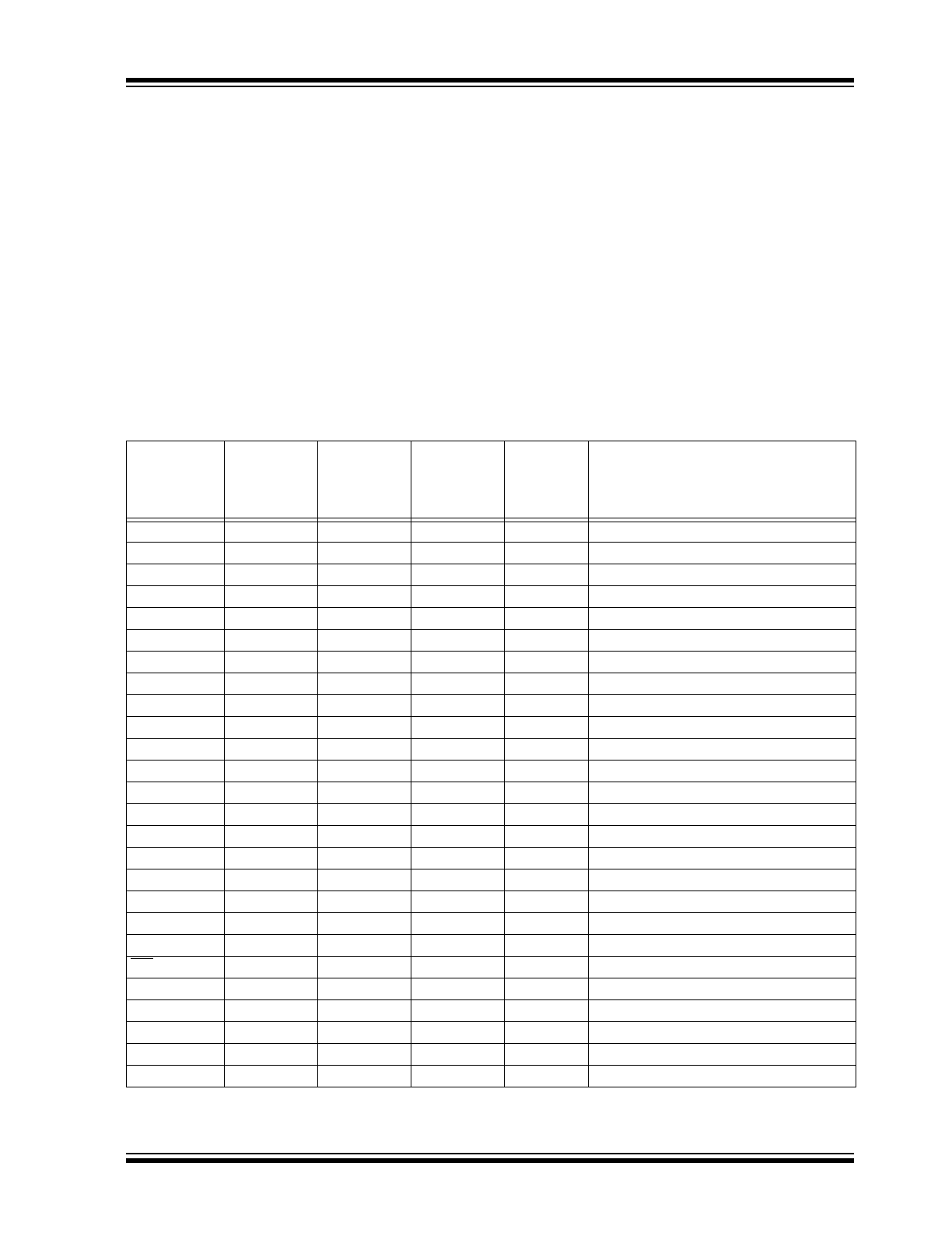
Pin Descriptions
TABLE 1-1:
PINOUT DESCRIPTION
Pin Name
PDIP,
SOIC,
SSOP
Pin No.
QFN
Pin No.
I/O/P
Type
Buffer
Type
Description
CLK
9
6
I
ST
Clock source input
TP
10
7
O
—
Test Pin (This pin must be left floating)
GP1.0
2
27
I/O
TTL
D0 digital input/output for GP1
GP1.1
3
28
I/O
TTL
D1 digital input/output for GP1
GP1.2
4
1
I/O
TTL
D2 digital input/output for GP1
GP1.3
5
2
I/O
TTL
D3 digital input/output for GP1
GP1.4
7
4
I/O
TTL
D4 digital input/output for GP1
GP1.5
11
8
I/O
ST
D5 digital input/output for GP1
GP1.6
12
9
I/O
ST
D6 digital input/output for GP1
GP1.7
13
10
I/O
ST
D7 digital input/output for GP1
GP0.0
21
18
I/O
TTL
D0 digital input/output for GP0
GP0.1
22
19
I/O
TTL
D1 digital input/output for GP0
GP0.2
23
20
I/O
TTL
D2 digital input/output for GP0
GP0.3
24
21
I/O
TTL
D3 digital input/output for GP0
GP0.4
25
22
I/O
TTL
D4 digital input/output for GP0
GP0.5
26
23
I/O
TTL
D5 digital input/output for GP0
GP0.6
27
24
I/O
TTL
D6 digital input/output for GP0
GP0.7
28
25
I/O
TTL
D7 digital input/output for GP0
SCL
14
11
I
ST
Serial clock input
SDA
15
12
I/O
ST
Serial data I/O
INT
6
3
O
OD
Interrupt output
A0
16
13
I
ST
Address input 1
A1
17
14
I
ST
Address input 2
A2
18
15
I
ST
Address input 3
V
SS
1, 8, 19
5, 16, 26
P
—
Ground reference for logic and I/O pins
V
DD
20
17
P
—
Positive supply for logic and I/O pins
MCP23016
DS20090C-page 4
©
2007 Microchip Technology Inc.
1.2
Power-on Reset (POR)
The on-chip POR circuit holds the chip in RESET until
V
DD
has reached a high enough level to deactivate the
POR circuit (i.e., release RESET). A maximum rise
time for V
DD
is specified in the electrical specifications.
When the device starts normal operation (exits the
RESET condition), device operating parameters
(voltage, frequency, temperature) must be met to
ensure proper operation.
1.3
Power-up Timer (PWRT)
The Power-up Timer provides a 72 ms nominal time-
out on power-up, keeping the device in RESET and
allowing V
DD
to rise to an acceptable level.
The power-up time delay will vary from chip-to-chip due
to V
DD
, temperature and process variation. See
Table 2-4 for details (T
PWRT
, parameter 3).
1.4
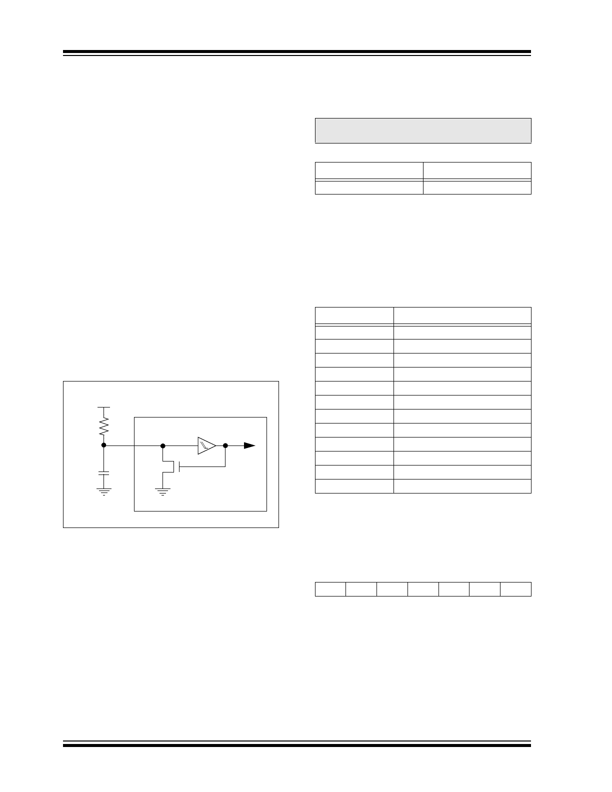
Clock Generator
The MCP23016 uses an external RC circuit to
determine the internal clock speed. The user must
connect R and C to the MCP23016, as shown in
Figure 1-1.
FIGURE 1-1:
CLOCK CONFIGURATION
A 1 MHz (typ.) internal clock is needed for the device to
function properly. The internal clock can be measured
on the TP pin. Recommended R
EXT
and C
EXT
values
are shown in Table 1-2.
1.5
I
2
C Bus Interface/ Protocol
Handler
This block manages the functionality of the I
2
C bus
interface and protocol handling. The MCP23016
supports the following commands:
TABLE 1-3:
COMMAND BYTE TO
REGISTER RELATIONSHIP
1.6
Address Decoder
The last three LSb of the 7-bit address are user-defined
(see Table 1-4). Three hardware pins (<A2:A0>) define
these bits.
TABLE 1-4:
DEVICE ADDRESS
Internal Clock
MCP23016
V
DD
R
EXT
C
EXT
V
SS
CLK
Note:
Set IARES =
1
to measure the clock
output on TP.
TABLE 1-2:
RECOMMENDED VALUES
R
EXT
C
EXT
3.9 k
Ω
33 pF
Command Byte
Result
0h
Access to GP0
1h
Access to GP1
2h
Access to OLAT0
3h
Access to OLAT1
4h
Access to IPOL0
5h
Access to IPOL1
6h
Access to IODIR0
7h
Access to IODIR1
8h
Access to INTCAP0 (Read-Only)
9h
Access to INTCAP1 (Read-Only)
Ah
Access to IOCON0
Bh
Access to IOCON1
0
1
0
0
A2
A1
A0
©
2007 Microchip Technology Inc.
DS20090C-page 5
MCP23016
1.7
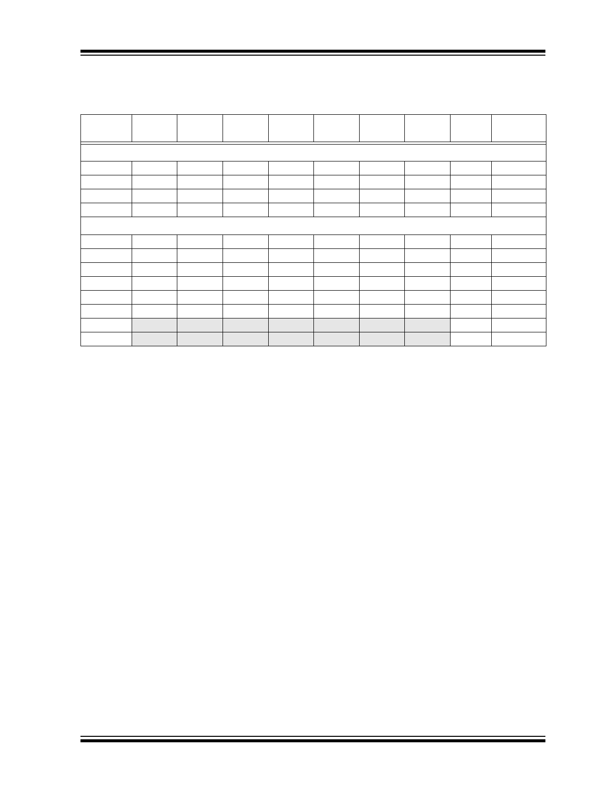
Register Block
The register block contains the Configuration and Port registers, as shown in Table 1-5.
TABLE 1-5:
REGISTER SUMMARY
Name
Bit 7
Bit 6
Bit 5
Bit 4
Bit 3
Bit 2
Bit 1
Bit 0
Value on
POR
Port Registers
GP0
GP0.7
GP0.6
GP0.5
GP0.4
GP0.3
GP0.2
GP0.1
GP0.0
0000 0000
GP1
GP1.7
GP1.6
GP1.5
GP1.4
GP1.3
GP1.2
GP1.1
GP0.0
0000 0000
OLAT0
OL0.7
OL0.6
OL0.5
OL0.4
OL0.3
OL0.2
OL0.1
OL0.0
0000 0000
OLAT1
OL1.7
OL1.6
OL1.5
OL1.4
OL1.3
OL1.2
OL1.1
OL1.0
0000 0000
Configuration Registers
IPOL0
IGP0.7
IGP0.6
IGP0.5
IGP0.4
IGP0.3
IGP0.2
IGP0.1
IGP0.0
0000 0000
IPOL1
IGP1.7
IGP1.6
IGP1.5
IGP1.4
IGP1.3
IGP1.2
IGP1.1
IGP1.0
0000 0000
IODIR0
IOD0.7
IOD0.6
IOD0.5
IOD0.4
IOD0.3
IOD0.2
IOD0.1
IOD0.0
1111 1111
IODIR1
IOD1.7
IOD1.6
IOD1.5
IOD1.4
IOD1.3
IOD1.2
IOD1.1
IOD1.0
1111 1111
INTCAP0
ICP0.7
ICP0.6
ICP0.5
ICP0.4
ICP0.3
ICP0.2
ICP0.1
ICP0.0
xxxx xxxx
INTCAP1
ICP1.7
ICP1.6
ICP1.5
ICP1.4
ICP1.3
ICP1.2
ICP1.1
ICP1.0
xxxx xxxx
IOCON0
—
—
—
—
—
—
—
IARES
---- ---0
IOCON1
—
—
—
—
—
—
—
IARES
---- ---0
Legend:
‘
1’ bit is set, ‘0’ bit is cleared, x = unknown, — = unimplemented.
MCP23016
DS20090C-page 6
©
2007 Microchip Technology Inc.
1.7.1
DATA PORT REGISTERS
Two registers provide access to the two GPIO ports:
• GP0 (provides access to data port GP0)
• GP1 (provides access to data port GP1)
A read from this register provides status on pins of
these ports. A write to these registers will modify the
output latch registers (OLAT0, OLAT1) and data output.
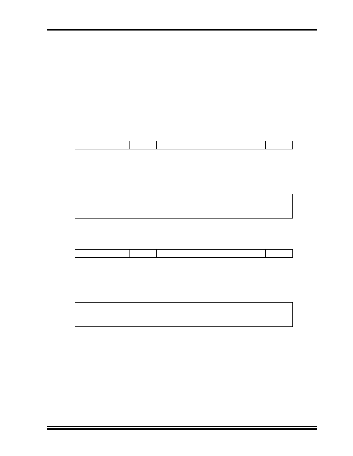
REGISTER 1-1:
GP0 - GENERAL PURPOSE I/O PORT REGISTER 0
REGISTER 1-2:
GP1 - GENERAL PURPOSE I/O PORT REGISTER 1
R/W-0
R/W-0
R/W-0
R/W-0
R/W-0
R/W-0
R/W-0
R/W-0
GP0.7
GP0.6
GP0.5
GP0.4
GP0.3
GP0.2
GP0.1
GP0.0
bit 7
bit 0
bit 7-0
GP0.0:GP0.7: Reflects the logic level on the pins.
1
= Logic ‘
1
’
0
= Logic ‘
0
’
Legend:
R = Readable bit
W = Writable bit
U = Unimplemented bit, read as ‘0’
- n = Value at POR
‘
1
’ = Bit is set
‘
0
’ = Bit is cleared
x = Bit is unknown
R/W-0
R/W-0
R/W-0
R/W-0
R/W-0
R/W-0
R/W-0
R/W-0
GP1.7
GP1.6
GP1.5
GP1.4
GP1.3
GP1.2
GP1.1
GP1.0
bit 7
bit 0
bit 7-0
GP1.0:GP1.7: Reflects the logic level on the pins.
1
= Logic ‘
1
’
0
= Logic ‘
0
’
Legend:
R = Readable bit
W = Writable bit
U = Unimplemented bit, read as ‘0’
- n = Value at POR
‘
1
’ = Bit is set
‘
0
’ = Bit is cleared
x = Bit is unknown
©
2007 Microchip Technology Inc.
DS20090C-page 7
MCP23016
1.7.2
OUTPUT LATCH REGISTERS
Two registers provide access to the two port output
latches:
• OLAT0 (provides access to the output latch for
port GP0)
• OLAT1 (provides access to the output latch for
port GP1)
A read from these registers results in a read of the latch
that controls the output and not the actual port. A write
to these registers updates the output latch that controls
the output.
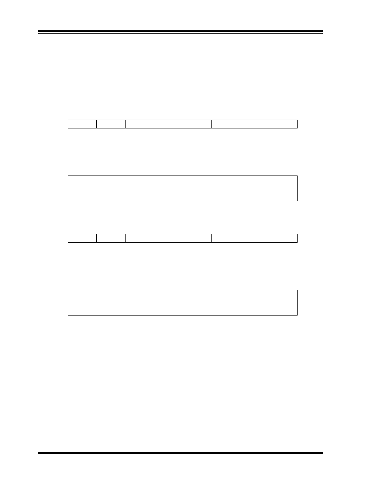
REGISTER 1-3:
OLAT0 - OUTPUT LATCH REGISTER 0
REGISTER 1-4:
OLAT1 - OUTPUT LATCH REGISTER 1
R/W-0
R/W-0
R/W-0
R/W-0
R/W-0
R/W-0
R/W-0
R/W-0
OL0.7
OL0.6
OL0.5
OL0.4
OL0.3
OL0.2
OL0.1
OL0.0
bit 7
bit 0
bit 7-0
OL0.0:O0.7: Reflects the logic level on the output latch.
1
= Logic ‘
1
’
0
= Logic ‘
0
’
Legend:
R = Readable bit
W = Writable bit
U = Unimplemented bit, read as ‘0’
- n = Value at POR
‘
1
’ = Bit is set
‘
0
’ = Bit is cleared
x = Bit is unknown
R/W-0
R/W-0
R/W-0
R/W-0
R/W-0
R/W-0
R/W-0
R/W-0
OL1.7
OL1.6
OL1.5
OL1.4
OL1.3
OL1.2
OL1.1
OL1.0
bit 7
bit 0
bit 7-0
OL1.0:O1.7: Reflects the logic level on the output latch.
1
= Logic ‘
1
’
0
= Logic ‘
0
’
Legend:
R = Readable bit
W = Writable bit
U = Unimplemented bit, read as ‘0’
- n = Value at POR
‘
1
’ = Bit is set
‘
0
’ = Bit is cleared
x = Bit is unknown
MCP23016
DS20090C-page 8
©
2007 Microchip Technology Inc.
1.7.3
INPUT POLARITY REGISTERS
These registers allow the user to configure the polarity
of the input port data (GP0 and GP1). If a bit in this reg-
ister is set, the corresponding input port (GPn) data bit
polarity will be inverted.
• IPOL0 (controls the polarity of GP0)
• IPOL1 (controls the polarity of GP1)
REGISTER 1-5:
IPOL0 - INPUT POLARITY PORT REGISTER 0
REGISTER 1-6:
IPOL1 - INPUT POLARITY PORT REGISTER 1
R/W-0
R/W-0
R/W-0
R/W-0
R/W-0
R/W-0
R/W-0
R/W-0
IGP0.7
IGP0.6
IGP0.5
IGP0.4
IGP0.3
IGP0.2
IGP0.1
IGP0.0
bit 7
bit 0
bit 7-0
IGP0.0:IGP0.7:
Controls the polarity inversion for the input pins
1
= Corresponding GP0 bit is inverted
0
= Corresponding GP0 bit is not inverted
Legend:
R = Readable bit
W = Writable bit
U = Unimplemented bit, read as ‘0’
- n = Value at POR
‘
1
’ = Bit is set
‘
0
’ = Bit is cleared
x = Bit is unknown
R/W-0
R/W-0
R/W-0
R/W-0
R/W-0
R/W-0
R/W-0
R/W-0
IGP1.7
IGP1.6
IGP1.6
IGP1.4
IGP1.3
IGP1.2
IGP1.1
IGP1.0
bit 7
bit 0
bit 7-0
IGP1.0:IGP1.7:
Controls the polarity inversion for the input pins
1
= Corresponding GP1 bit is inverted
0
= Corresponding GP1 bit is not inverted
Legend:
R = Readable bit
W = Writable bit
U = Unimplemented bit, read as ‘0’
- n = Value at POR
‘
1
’ = Bit is set
‘
0
’ = Bit is cleared
x = Bit is unknown
©
2007 Microchip Technology Inc.
DS20090C-page 9
MCP23016
1.7.4
I/O DIRECTION REGISTERS
Two registers control the direction of data I/O:
• IODIR0 (controls GP0)
• IODIR1 (controls GP1)
When a bit in these registers is set, the corresponding
pin becomes an input. Otherwise, it becomes an
output. At Power-on Reset, the device ports are
configured as inputs.
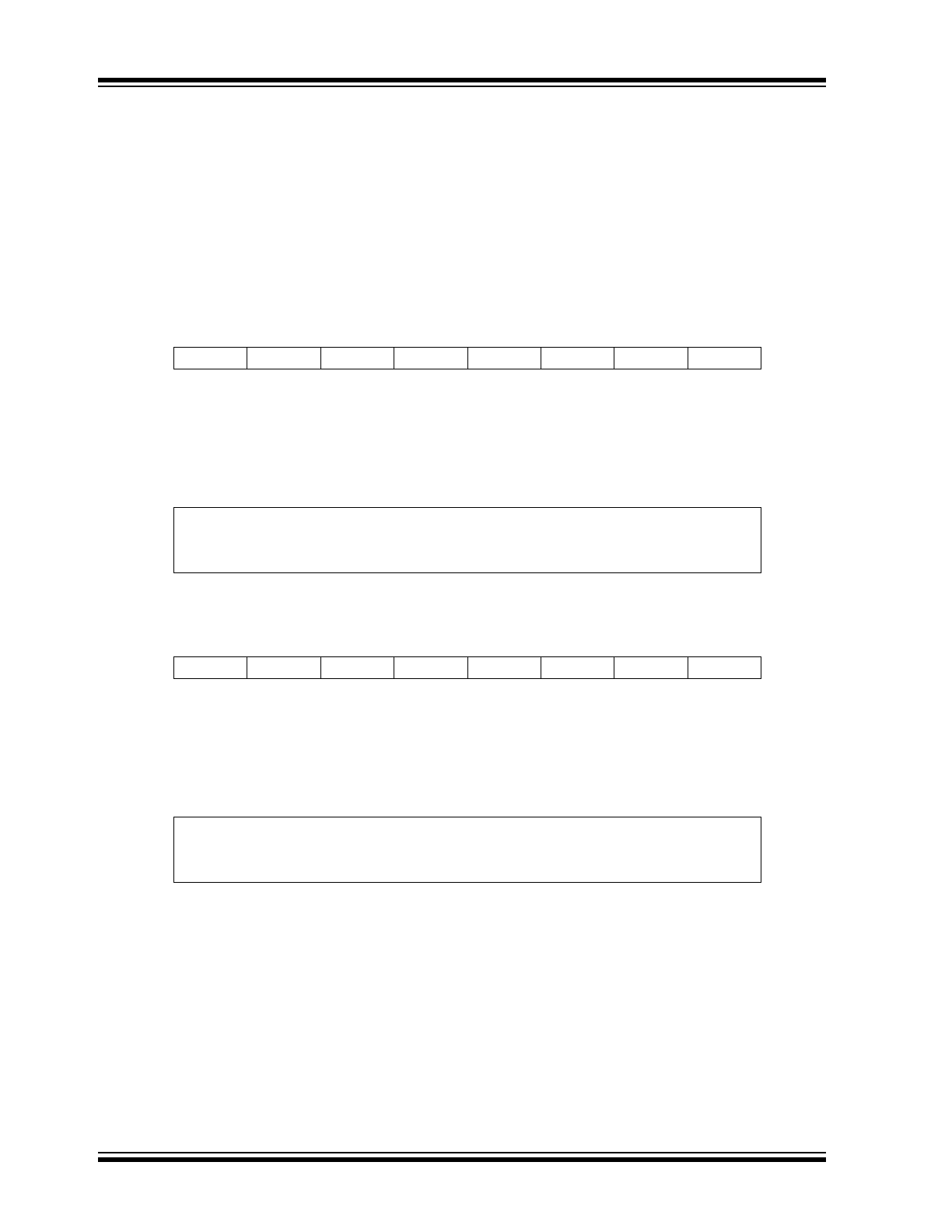
REGISTER 1-7:
IODIR0 - I/O DIRECTION REGISTER 0
REGISTER 1-8:
IODIR1 - I/O DIRECTION REGISTER 1
R/W-1
R/W-1
R/W-1
R/W-1
R/W-1
R/W-1
R/W-1
R/W-1
IOD0.7
IOD0.6
IOD0.5
IOD0.4
IOD0.3
IOD0.2
IOD0.1
IOD0.0
bit 7
bit 0
bit 7-0
IOD0.0:IO0.7:
Controls the direction of data I/O
1
= Input
0
= Output
Legend:
R = Readable bit
W = Writable bit
U = Unimplemented bit, read as ‘0’
- n = Value at POR
‘
1
’ = Bit is set
‘
0
’ = Bit is cleared
x = Bit is unknown
R/W-1
R/W-1
R/W-1
R/W-1
R/W-1
R/W-1
R/W-1
R/W-1
IOD1.7
IOD1.6
IOD1.5
IOD1.4
IOD1.3
IOD1.2
IOD1.1
IOD1.0
bit 7
bit 0
bit 7-0
IOD1.0:IO1.7:
Controls the direction of data I/O
1
= Input
0
= Output
Legend:
R = Readable bit
W = Writable bit
U = Unimplemented bit, read as ‘0’
- n = Value at POR
‘
1
’ = Bit is set
‘
0
’ = Bit is cleared
x = Bit is unknown
MCP23016
DS20090C-page 10
©
2007 Microchip Technology Inc.
1.7.5
INTERRUPT CAPTURE REGISTERS
Two registers contain the value of the port that
generated the interrupt:
• INTCAP0 contains the value of GP0 at time of
GP0 change interrupt
• INTCAP1 contains the value of GP1 at time of
GP1 change interrupt
These registers are ‘read-only’ registers (A write to
these registers is ignored).
REGISTER 1-9:
INTCAP0 - INTERRUPT CAPTURED VALUE FOR PORT REGISTER 0
REGISTER 1-10:
INTCAP1 - INTERRUPT CAPTURED VALUE FOR PORT REGISTER 1
R-x
R-x
R-x
R-x
R-x
R-x
R-x
R-x
ICP0.7
ICP0.6
ICP0.5
ICP0.4
ICP0.3
ICP0.2
ICP0.1
ICP0.0
bit 7
bit 0
bit 7-0
ICP0.0:ICP0.7:
Reflects the logic level on the GP0 pins at the time of interrupt due to pin
change
1
= Logic ‘
1
’
0
= Logic ‘
0
’
Legend:
R = Readable bit
W = Writable bit
U = Unimplemented bit, read as ‘0’
- n = Value at POR
‘
1
’ = Bit is set
‘
0
’ = Bit is cleared
x = Bit is unknown
R-x
R-x
R-x
R-x
R-x
R-x
R-x
R-x
ICP1.7
ICP1.6
ICP1.5
ICP1.4
ICP1.3
ICP1.2
ICP1.1
ICP1.0
bit 7
bit 0
bit 7-0
ICP1.0:ICP1.7:
Reflects the logic level on the GP1 pins at the time of interrupt due to pin
change
1
= Logic ‘
1
’
0
= Logic ‘
0
’
Legend:
R = Readable bit
W = Writable bit
U = Unimplemented bit, read as ‘0’
- n = Value at POR
‘
1
’ = Bit is set
‘
0
’ = Bit is cleared
x = Bit is unknown