
2009-2014 Microchip Technology Inc.
DS20002121C-page 1
MCP23009/MCP23S09
Features:
• 8-Bit Remote Bidirectional I/O Port:
- I/O Pins Default to Input
• Open-Drain Outputs:
- 5.5V Tolerant
- 25 mA Sink Capable (per Pin)
- 200 mA Total
• High-Speed I
2
C™ Interface (MCP23009):
- 100 kHz
- 400 kHz
- 3.4 MHz
• High-Speed SPI Interface (MCP23S09):
- 10 MHz
• Single Hardware Address Pin (MCP23009):
- Voltage input to allow up to eight devices on
the bus
• Configurable Interrupt Output Pins:
- Configurable as active-high, active-low or
open-drain
• Configurable Interrupt Source:
- Interrupt-on-Change from configured defaults
or pin change
• Polarity inversion register to configure the polarity
of the input port data
• External Reset Input
• Low Standby Current:
- 1 µA (-40°C
T
A
+85°C)
- 6 µA (+85°C
T
A
+125°C)
• Operating Voltage:
- 1.8V to 5.5V
• Available Packages:
- 16-Lead QFN (3x3x0.9 mm)
- 18-Lead PDIP (300 mil)
- 18-Lead SOIC (7.50 mm)
- 20-Lead SSOP (5.30 mm)
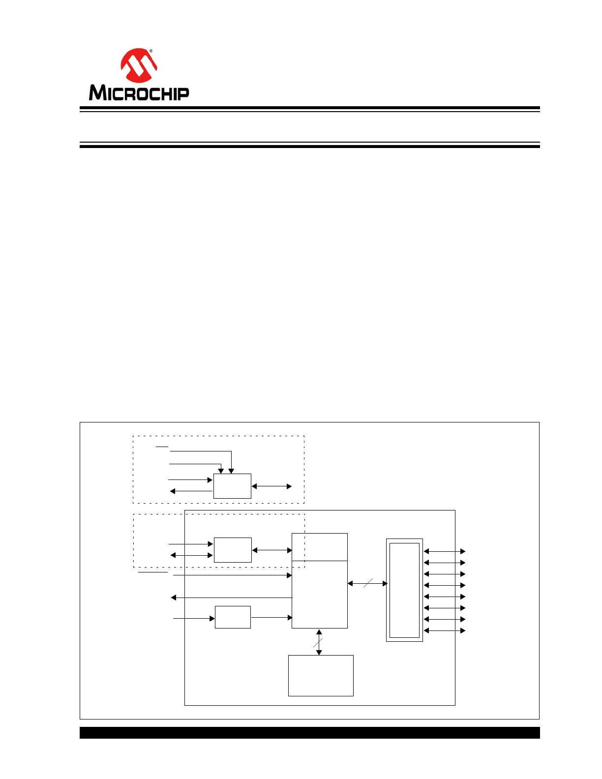
Block Diagram
GP0
GP1
GP2
GP3
GP4
GP5
GP6
GP7
I
2
C™
Control
GPIO
SCL
SDA
RESET
INT
8
Configuration/
8
Control
Registers
SPI
SI
SO
SCK
CS
MCP23S09
ADDR
Serializer/
Deserializer
Multi-Bit
Decode
MCP23009
8-Bit I/O Expander with Open-Drain Outputs
MCP23009/MCP23S09
DS20002121C-page 2
2009-2014 Microchip Technology Inc.
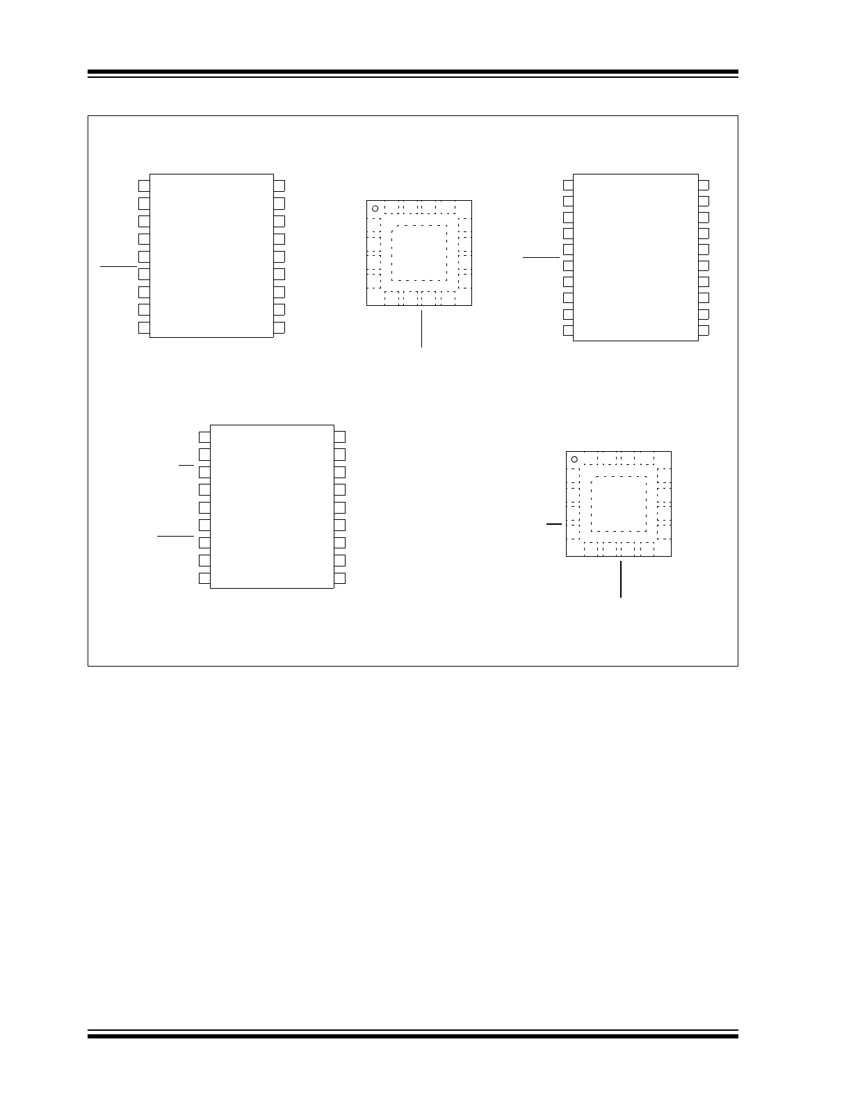
Package Types
V
SS
18
NC
17
NC
16
GP7
15
GP6
14
GP5
13
GP4
12
GP2
10
V
DD
1
NC
2
SCL
3
SDA
4
ADDR
5
RESET
6
INT
7
GP0
8
GP3
11
GP1
9
V
SS
20
NC
19
NC
18
GP7
17
GP6
16
GP5
15
GP4
14
GP3
13
GP2
12
NC
11
V
DD
1
NC
2
SCL
3
SDA
4
ADDR
5
RESET
6
INT
7
GP0
8
GP1
9
NC
10
V
SS
18
NC
17
GP7
16
GP6
15
GP5
14
GP4
13
GP3
12
GP1
10
V
DD
1
NC
2
CS
3
SCK
4
SI
5
SO
6
RESET
7
INT
8
GP2
11
GP0
9
* Includes Exposed Thermal Pad (EP); see
Tables 1-1
and
1-2
.
MCP23009
PDIP, SOIC
MCP23009
3 x 3 QFN*
MCP23009
SSOP
MCP23S09
PDIP/SOIC
MCP23S09
3 x 3 QFN*
2
V
DD
CS
V
SS
GP3
GP2
SI
GP1
SO
RE
S
E
T
INT
GP0
GP
7
GP
6
GP
5
GP
4
SCK
EP
16
1
15 14 13
3
4
12
11
10
9
5
6
7
8
17
2
V
DD
SCL
V
SS
GP3
GP2
SD
A
GP1
AD
D
R
RE
S
E
T
INT
GP0
GP
7
GP
6
GP
5
GP
4
NC
EP
16
1
15 14 13
3
4
12
11
10
9
5
6
7
8
17

2009-2014 Microchip Technology Inc.
DS20002121C-page 3
MCP23009/MCP23S09
1.0
DEVICE OVERVIEW
The MCP23X09 device provides 8-bit, general purpose
parallel I/O expansion for I
2
C bus or SPI applications.
The two devices differ only in the serial interface.
• MCP23009 – I
2
C interface
• MCP23S09 – SPI interface
The MCP23X09 consists of multiple 8-bit configuration
registers for input, output and polarity selection. The
system master can enable the I/Os as either inputs or
outputs by writing the I/O configuration bits. The data
for each input or output is kept in the corresponding
input or output register. The polarity of the input port
register can be inverted with the polarity inversion
register. All registers can be read by the system master.
The interrupt output can be configured to activate
under two conditions (mutually exclusive):
1.
When any input state differs from its
corresponding input port register state. This is
used to indicate to the system master that an
input state has changed.
2.
When an input state differs from a
pre-configured register value (DEFVAL
register).
The Interrupt Capture register captures port values at
the time of the Interrupt, thereby saving the condition
that caused the Interrupt.
The Power-On Reset (POR) sets the registers to their
default values and initializes the device state machine.
The hardware address pin is used to determine the
device address.

MCP23009/MCP23S09
DS20002121C-page 4
2009-2014 Microchip Technology Inc.
1.1
Pin Descriptions
TABLE 1-1:
I
2
C™ PINOUT DESCRIPTION (MCP23009)
Pin
Name
Pin Number
Pin
Type
Standard Function
16-lead
QFN
18-lead
PDIP/SOIC
20-lead
SSOP
V
DD
3
1
1
P
Power
NC
2
2, 16-17
2, 10-11,
18-19
—
Not connected
SCL
4
3
3
I
Serial clock input
SDA
5
4
4
I/O
Serial data I/O
ADDR
6
5
5
I
Hardware address pin allows up to eight slave devices on the
bus
RESET
7
6
6
I
Hardware reset
INT
8
7
7
O
Interrupt output for port. Can be configured as active-high,
active-low or open-drain.
GP0
9
8
8
I/O
Bidirectional I/O pin (5.5V tolerant inputs; open-drain outputs).
Can be enabled for interrupt on change and/or internal pull-up
resistor.
GP1
10
9
9
I/O
Bidirectional I/O pin (5.5V tolerant inputs; open-drain outputs).
Can be enabled for interrupt on change and/or internal pull-up
resistor.
GP2
11
10
12
I/O
Bidirectional I/O pin (5.5V tolerant inputs; open-drain outputs).
Can be enabled for interrupt on change and/or internal pull-up
resistor.
GP3
12
11
13
I/O
Bidirectional I/O pin (5.5V tolerant inputs; open-drain outputs).
Can be enabled for interrupt on change and/or internal pull-up
resistor.
GP4
13
12
14
I/O
Bidirectional I/O pin (5.5V tolerant inputs; open-drain outputs).
Can be enabled for interrupt on change and/or internal pull-up
resistor.
GP5
14
13
15
I/O
Bidirectional I/O pin (5.5V tolerant inputs; open-drain outputs).
Can be enabled for interrupt on change and/or internal pull-up
resistor.
GP6
15
14
16
I/O
Bidirectional I/O pin (5.5V tolerant inputs; open-drain outputs).
Can be enabled for interrupt on change and/or internal pull-up
resistor.
GP7
16
15
17
I/O
Bidirectional I/O pin (5.5V tolerant inputs; open-drain outputs).
Can be enabled for interrupt on change and/or internal pull-up
resistor.
V
SS
1
18
20
P
Ground
EP
17
—
—
—
Exposed Thermal Pad (EP). Can be left floating or connected
to V
SS
.

2009-2014 Microchip Technology Inc.
DS20002121C-page 5
MCP23009/MCP23S09
TABLE 1-2:
SPI PINOUT DESCRIPTION (MCP23S09)
Pin
Name
Pin Number
Pin
Type
Standard Function
16-lead
QFN
18-lead
PDIP/SOIC
V
DD
3
1
P
Power (high-current capable)
NC
—
2, 17
—
Not connected
CS
4
3
I
Chip select
SCK
2
4
I
Serial clock input
SI
5
5
I
Serial data input
SO
6
6
O
Serial data out
RESET
7
7
I
Hardware reset (must be externally biased)
INT
8
8
O
Interrupt output for port. Can be configured as active-high, active-low or
open-drain.
GP0
9
9
I/O
Bidirectional I/O pin (5.5V tolerant inputs; open-drain outputs). Can be
enabled for Interrupt-on-Change and/or internal pull-up resistor.
GP1
10
10
I/O
Bidirectional I/O pin (5.5V tolerant inputs; open-drain outputs). Can be
enabled for Interrupt-on-Change and/or internal pull-up resistor.
GP2
11
11
I/O
Bidirectional I/O pin (5.5V tolerant inputs; open-drain outputs). Can be
enabled for Interrupt-on-Change and/or internal pull-up resistor.
GP3
12
12
I/O
Bidirectional I/O pin (5.5V tolerant inputs; open-drain outputs). Can be
enabled for Interrupt-on-Change and/or internal pull-up resistor.
GP4
13
13
I/O
Bidirectional I/O pin (5.5V tolerant inputs; open-drain outputs). Can be
enabled for Interrupt-on-Change and/or internal pull-up resistor.
GP5
14
14
I/O
Bidirectional I/O pin (5.5V tolerant inputs; open-drain outputs). Can be
enabled for Interrupt-on-Change and/or internal pull-up resistor.
GP6
15
15
I/O
Bidirectional I/O pin (5.5V tolerant inputs; open-drain outputs). Can be
enabled for Interrupt-on-Change and/or internal pull-up resistor.
GP7
16
16
I/O
Bidirectional I/O pin (5.5V tolerant inputs; open-drain outputs). Can be
enabled for Interrupt-on-Change and/or internal pull-up resistor.
V
SS
1
18
P
Ground (high-current capable)
EP
17
—
—
Exposed Thermal Pad (EP). Can be left floating or connected to V
SS
.

MCP23009/MCP23S09
DS20002121C-page 6
2009-2014 Microchip Technology Inc.
1.2
Power-On Reset (POR)
The on-chip POR circuit holds the device in reset until
V
DD
has reached a high enough voltage to deactivate
the POR circuit (i.e., release the device from reset).
The maximum V
DD
rise time is specified in the
electrical specification section.
When the device exits the POR condition (releases
reset), the device operating parameters (i.e., voltage,
temperature, serial bus frequency, etc.) must be met to
ensure proper operation.
1.3
Serial Interface
This block handles the functionality of the I
2
C
(MCP23009) or SPI (MCP23S09) interface protocol.
The MCP23X09 contains eleven (11) individual
registers which can be addressed through the Serial
Interface block (
Table 1-3
).
TABLE 1-3:
REGISTER ADDRESSES
1.3.1
BYTE MODE AND SEQUENTIAL
MODE
The MCP23X09 has the ability to operate in Byte mode
or Sequential mode (IOCON.SEQOP). Byte mode and
Sequential mode are not to be confused with I
2
C byte
operations and sequential operations. The modes
explained here relate to the device’s internal address
pointer and whether or not it is incremented after each
byte is clocked on the serial interface.
• Byte mode disables automatic address pointer
incrementing. When operating in Byte mode, the
MCP23X09 does not increment its internal
address counter after each byte during the data
transfer. This gives the ability to continually
access the same address by providing extra
clocks (without additional control bytes). This is
useful for polling the GPIO register for data
changes or for continually writing to the output
latches.
• Sequential mode enables automatic address
pointer incrementing. When operating in
Sequential mode, the MCP23X09 increments its
address counter after each byte during the data
transfer. The address pointer automatically rolls
over to address 00h after accessing the last
register.
These two modes are not to be confused with single
writes/reads and continuous writes/reads, which are
serial protocol sequences. For example, the device
may be configured for Byte mode and the master may
perform a continuous read. In this case, the
MCP23X09 would not increment the address pointer
and would repeatedly drive data from the same
location.
1.3.2
I
2
C INTERFACE
1.3.2.1
I
2
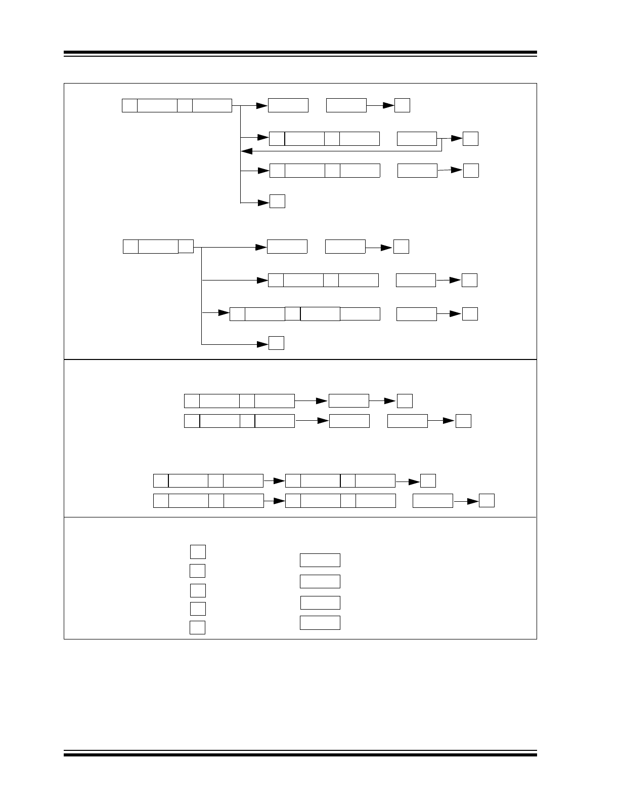
C Write Operation
The I
2
C write operation includes the control byte and
the register address sequence, as shown in the bottom
of
Figure 1-1
. This sequence is followed by eight bits of
data from the master and an Acknowledge (ACK) from
the MCP23009. The operation is ended with a Stop (P)
or Restart (SR) condition being generated by the
master.
Data is written to the MCP23009 after every byte
transfer. If a Stop or Restart condition is generated
during a data transfer, the data will not be written to the
MCP23009.
Both Byte mode and Sequential mode are supported
by the MCP23009. If Sequential mode is enabled
(default), the MCP23009 increments its address
counter after each ACK during the data transfer.
1.3.2.2
I
2
C Read Operation
I
2
C read operations include the control byte sequence,
as shown in the bottom of
Figure 1-1
. This sequence is
followed by another control byte (including the Start
condition and ACK) with the R/W bit equal to a logic
one (R/W = 1). The MCP23009 then transmits the data
contained in the addressed register. The sequence is
ended with the master generating a Stop or Restart
condition.
1.3.2.3
I
2
C Sequential Write/Read
For sequential operations (Write or Read), instead of
transmitting a Stop or Restart condition after the data
transfer, the master clocks the next byte pointed to by
the address pointer (see
Section 1.3.1 “Byte Mode
and Sequential Mode”
for details regarding sequential
operation control).
The sequence ends with the master sending a Stop or
Restart condition.
The MCP23009 address pointer will roll over to
address zero after reaching the last register address.
Refer to
Figure 1-1
.
Address
Access to
00h
IODIR
01h
IPOL
02h
GPINTEN
03h
DEFVAL
04h
INTCON
05h
IOCON
06h
GPPU
07h
INTF
08h
INTCAP (read-only)
09h
GPIO
0Ah
OLAT

2009-2014 Microchip Technology Inc.
DS20002121C-page 7
MCP23009/MCP23S09
1.3.3
SPI INTERFACE
The MCP23S09 operates in Mode 0,0 and Mode 1,1.
The difference between the two modes is the idle state
of the clock.
• Mode 0,0: The idle state of the clock is low. Input
data is latched on the rising edge of the clock; out-
put data is driven on the falling edge of the clock.
• Mode 1,1: The idle state of the clock is high. Input
data is latched on the rising edge of the clock; out-
put data is driven on the falling edge of the clock.
1.3.3.1
SPI Write Operation
The SPI write operation is started by lowering CS. The
write command (slave address with R/W bit cleared) is
then clocked into the device. The opcode is followed by
an address and at least one data byte.
1.3.3.2
SPI Read Operation
The SPI read operation is started by lowering CS. The
SPI read command (slave address with R/W bit set) is
then clocked into the device. The opcode is followed by
an address, with at least one data byte being clocked
out of the device.
1.3.3.3
SPI Sequential Write/Read
For sequential operations, instead of deselecting the
device by raising CS, the master clocks the next byte
pointed to by the address pointer (see
Section 1.3.1
“Byte Mode and Sequential Mode”
for details
regarding sequential operation control).
The sequence ends by the raising of CS.
The MCP23S09 address pointer will roll over to
address zero after reaching the last register address.
MCP23009/MCP23S09
DS20002121C-page 8
2009-2014 Microchip Technology Inc.
FIGURE 1-1:
MCP23009 I
2
C™ DEVICE PROTOCOL
S
P
SR
W
R
OP
ADDR
D
IN
D
IN
....
S
P
W
R
OP
ADDR
D
OUT
D
OUT
....
P
SR
W
OP
ADDR
D
IN
....
P
P
SR
R
D
OUT
D
OUT
....
P
OP
D
OUT
D
OUT
....
P
SR
OP
D
IN
....
P
OP
D
IN
S
P
W
OP
ADDR
D
IN
D
IN
....
Byte and Sequential Write
S
W
OP
SR
R
OP
D
OUT
D
OUT
....
P
Byte and Sequential Read
S
W
OP
ADDR
D
IN
P
S
W
OP
SR
R
OP
D
OUT
P
Byte
Sequential
Byte
Sequential
ADDR
ADDR
S
P
SR
W
R
OP
ADDR
D
OUT
D
IN
- Start
- Restart
- Stop
- Write
- Read
- Device opcode
- Device address
- Data out from MCP23009
- Data in to MCP23009
Legend:
2009-2014 Microchip Technology Inc.
DS20002121C-page 9
MCP23009/MCP23S09
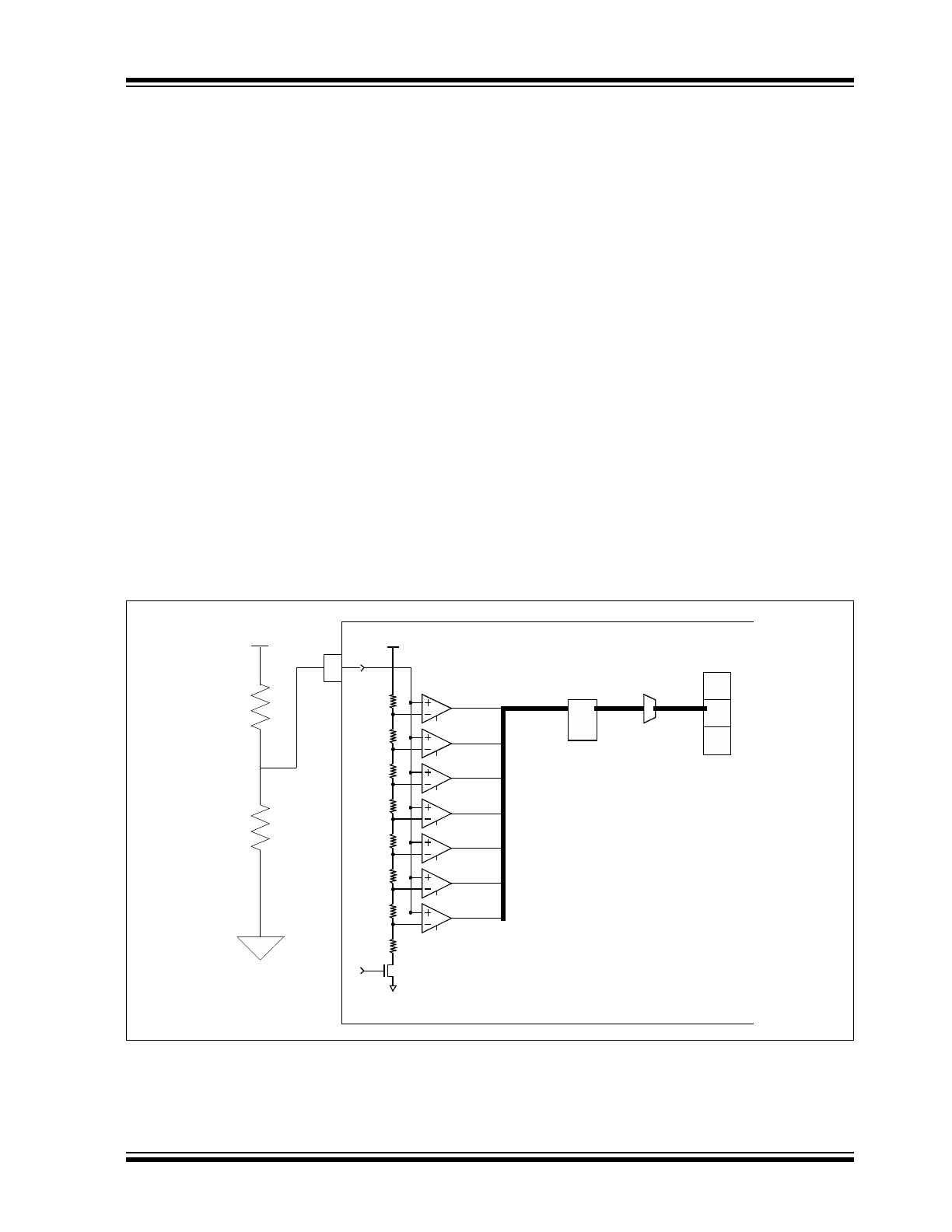
1.4
Multi-Bit Address Decoder
The ADDR pin is used to set the slave address of the
MCP23009 (I
2
C only) to allow up to eight devices on
the bus using only a single pin. Typically, this would
require three pins.
The multi-bit Address Decoder employs a basic FLASH
ADC architecture (
Figure 1-4
). The seven comparators
generate eight unique values based on the analog
input. This value is converted to a 3-bit code which
corresponds to the address bits (A2, A1, A0) in the
serial OPCODE.
Sequence of operation (see
Figure 1-5
for
timings):
1.
Upon power-up (after V
DD
stabilizes), the
module becomes active after time t
ADEN
. Note
that the analog value on the ADDR pin must be
stable before this point to ensure accurate
address assignment.
2.
The 3-bit address is latched after t
ADDRLAT
.
3.
The module powers down after the first rising
edge of the serial clock is detected (t
ADDIS
).
Once the address bits are latched, the device will keep
the slave address until a POR or Reset condition
occurs.
1.4.1
CALCULATING VOLTAGE ON ADDR
When calculating the required voltage on the ADDR pin
(V2), the set point should be the mid point of the LSb of
the ADC.
The examples in
Figures 1-2
and
1-3
show how to
determine the mid-point voltage (V2) and the range of
voltages based on a voltage divider circuit. The
maximum tolerance is 20%, however, it is
recommended to use 5% tolerance worst-case (10%
total tolerance).
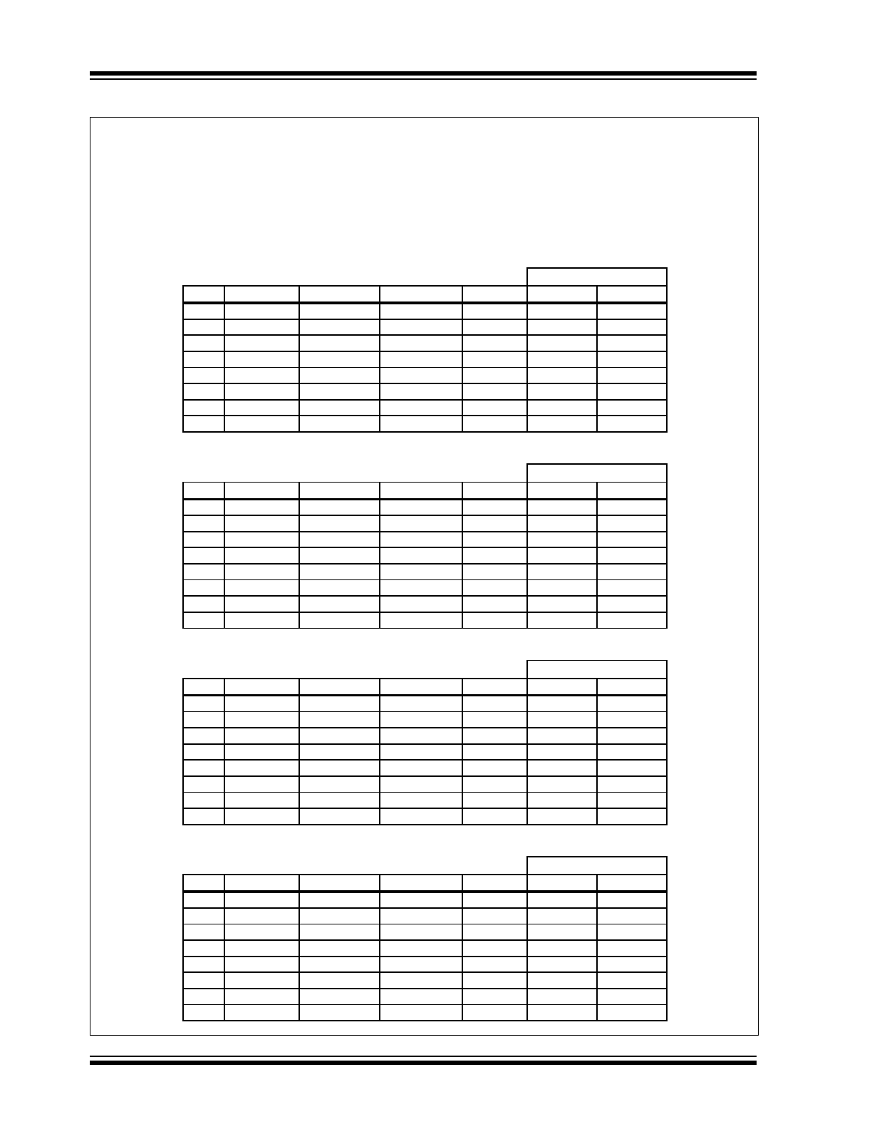
FIGURE 1-2:
VOLTAGE DIVIDER EXAMPLE
R2
A0
A1
A2
V2
R1
V
DD
MCP23009 Only
V
DD
V
SS
V
SS
ADDR
MCP23009/MCP23S09
DS20002121C-page 10
2009-2014 Microchip Technology Inc.
FIGURE 1-3:
VOLTAGE AND CODE EXAMPLE
Assume:
n = A2, A1, A0 in opcode
ratio = R2/(R1+R2)
V2 = voltage on ADDR pin
V2(min) = V2 – (V
DD
/8) x %tolerance
V2(max) = V2 + (V
DD
/8) x %tolerance
V
DD
= 1.8
n
R2 = 2n + 1 R1 = 16 – R2 R2/(R1 + R2)
V2
V2(min)
V2(max)
0
1
15
0.0625
0.113
0.00
0.14
1
3
13
0.1875
0.338
0.32
0.36
2
5
11
0.3125
0.563
0.54
0.59
3
7
9
0.4375
0.788
0.77
0.81
4
9
7
0.5625
1.013
0.99
1.04
5
11
5
0.6875
1.238
1.22
1.26
6
13
3
0.8125
1.463
1.44
1.49
7
15
1
0.9375
1.688
1.67
1.80
V
DD
= 2.7
n
R2 = 2n + 1 R1 = 16 – R2 R2/(R1 + R2)
V2
V2(min)
V2(max)
0
1
15
0.0625
0.169
0.00
0.19
1
3
13
0.1875
0.506
0.48
0.53
2
5
11
0.3125
0.844
0.82
0.87
3
7
9
0.4375
1.181
1.16
1.20
4
9
7
0.5625
1.519
1.50
1.54
5
11
5
0.6875
1.856
1.83
1.88
6
13
3
0.8125
2.194
2.17
2.22
7
15
1
0.9375
2.531
2.51
2.70
V
DD
= 3.3
n
R2 = 2n + 1 R1 = 16 – R2 R2/(R1 + R2)
V2
V2(min)
V2(max)
0
1
15
0.0625
0.206
0.00
0.23
1
3
13
0.1875
0.619
0.60
0.64
2
5
11
0.3125
1.031
1.01
1.05
3
7
9
0.4375
1.444
1.42
1.47
4
9
7
0.5625
1.856
1.83
1.88
5
11
5
0.6875
2.269
2.25
2.29
6
13
3
0.8125
2.681
2.66
2.70
7
15
1
0.9375
3.094
3.07
3.30
V
DD
= 5.5
n
R2 = 2n + 1 R1 = 16 – R2 R2/(R1 + R2)
V2
V2(min)
V2(max)
0
1
15
0.0625
0.344
0.00
0.37
1
3
13
0.1875
1.031
1.01
1.05
2
5
11
0.3125
1.719
1.70
1.74
3
7
9
0.4375
2.406
2.38
2.43
4
9
7
0.5625
3.094
3.07
3.12
5
11
5
0.6875
3.781
3.76
3.80
6
13
3
0.8125
4.469
4.45
4.49
7
15
1
0.9375
5.156
5.13
5.50
10% Tolerance (total)
10% Tolerance (total)
10% Tolerance (total)
10% Tolerance (total)