

2014-2017 Microchip Technology Inc.
DS20005292C-page 1
MCP2221
Features
Universal Serial Bus (USB)
• Supports Full-Speed USB (12 Mb/s)
• Implements USB Protocol Composite Device:
- Communication Device Class (CDC) for
USB-to-UART Conversion
- Human Interface Device (HID) for I
2
C Device
Control and Configuration
• 128-Byte Buffer to Handle Data Throughput at
Any Supported UART Baud Rate:
- 64-Byte Transmit
- 64-Byte Receive
• Human Interface Device (HID) for Both
I
2
C Communication and Control:
64-Byte Buffer to Handle Data Throughput at
Any I
2
C Baud Rate
• Fully-Configurable VID and PID Assignments and
String Descriptors
• Bus-Powered or Self-Powered
• USB 2.0-Compliant: TID# 40001594
USB Driver and Software Support
• Enumerates as a Composite USB Device (CDC
and HID) Using Standard Drivers for Virtual Com
Port (VCP) on the Following Windows
®
Operating
Systems: XP
®
(SP3), Vista
®
, 7, 8 and 8.1
• Configuration Utility for Establishing a Custom
Boot-Up Configuration
• I
2
C/SMBus Terminal
• Windows DLL
CDC and Universal Asynchronous
Receiver/Transmitter (UART) Options
• Communications Device Class (CDC) for the
USB-to-UART Option
• Responds to SET LINE CODING Commands to
Dynamically Change Baud Rates
• Supports Baud Rates: 300-115200
• UART T
X
and R
X
Pins Only
• Serial Number Used During the CDC
Enumeration Can Be Enabled by Using the
Microchip-Provided Configuration Utility or by
Calling the Proper API from the Support Libraries
for this Device
I
2
C/SMBus
• The Device Runs as an I
2
C Master. The Data to
Write/Read on the I
2
C Bus is Conveyed by the
USB Interface
• I
2
C Master
- Up to 400 kHz Clock Rate
- Supports 7-Bit or 10-Bit Addressable
Devices; 10-Bit Addressable Devices are
Supported through the PC Host Library
- Supports Block Reads/Writes of up to 65,535
Bytes
• SMBus Master
- Supports All of the SMBus Transfers
- SMBus Functionality Is Achieved through a
Combination of Chip and Support Library
Processing
- Up to 400 kHz Clock Rate
General-Purpose Input/Output (GPIO) Pins
• Four General-Purpose Input/Output Pins
• All GP Pins Can Be Assigned to Other
Functionalities
Other Functionalities
• UART Activity LED Outputs (UT
X
and UR
X
)
• SSPND Output Pin
• USBCFG Output Pin (Indicates When the
Enumeration Has Completed)
• Three ADC Inputs
• One DAC with Two Possible Output Options
• Clock Reference Output: 12 MHz or Other
Configurable Values
• External Interrupt Edge Detection
Other
• Operating Voltage: 3.0 to 5.5V
• Electrostatic Discharge (ESD) Protection: > 4 kV
Human Body Model (HBM)
• Industrial (I) Operating Temperature: –40°C to
+85°C
• Automotive AEC-Q100 Qualified
USB 2.0 to I
2
C/UART Protocol Converter with GPIO
MCP2221
DS20005292C-page 2
2014-2017 Microchip Technology Inc.
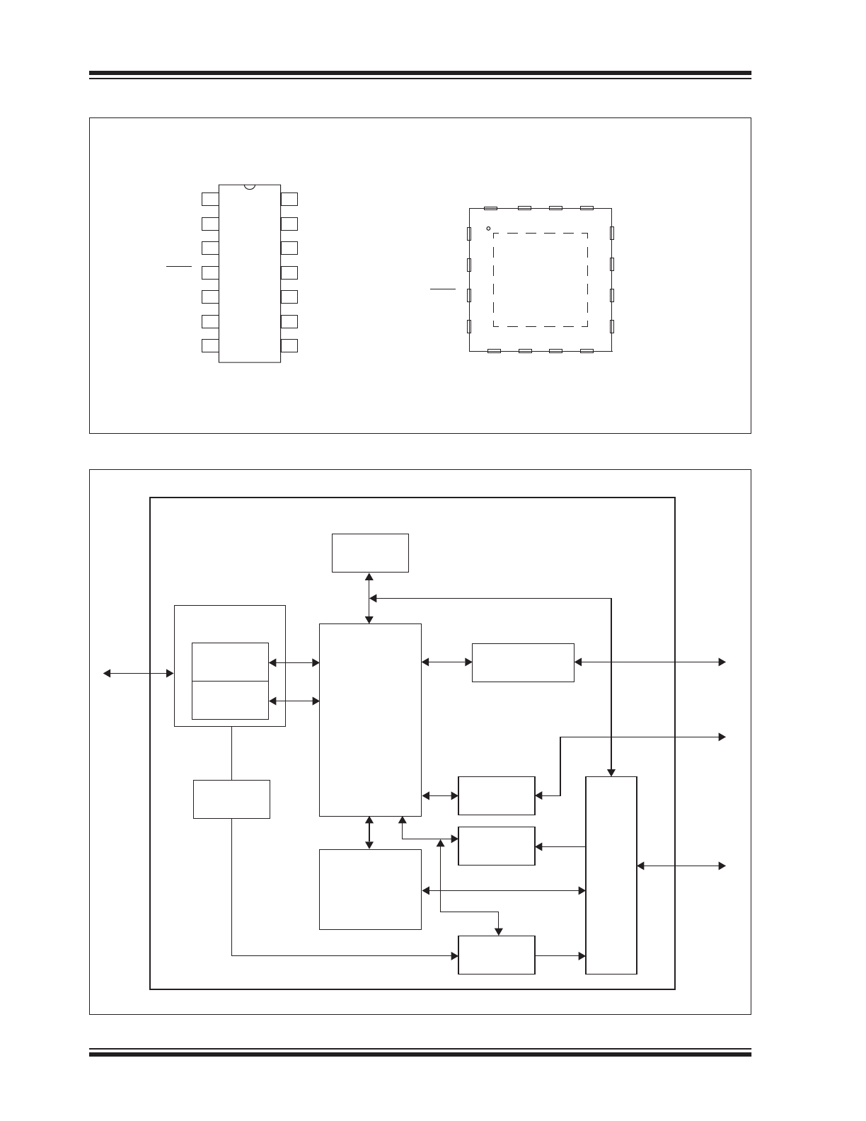
Package Types
Block Diagram
D-
D+
V
SS
V
DD
MCP2221
PDIP/SOIC/TSSOP
1
2
3
4
5
6
7
14
13
12
11
10
9
8
V
USB
RST
UR
X
UT
X
GP2
GP3
SDA
SCL
MCP2221
4 x 4 QFN*
1
2
4
3
5
6
7
8
9
10
11
12
13
14
15
16
EP
V
DD
NC
UT
X
GP2
GP3
SDA
SCL
V
USB
D-
D+
V
SS
NC
GP1
GP0
UR
X
RST
GP1
GP0
17
* Includes Exposed Thermal Pad (EP); see
Table 1-1
.
USB HID
USB CDC
CONFIG
I
2
C Master
UART
BUS MATRIX
GPIO
ADC/DAC
USB
Bus
I
2
C
Bus
T
X
D/R
X
D
GP Pins
PIN
MUX
IOC
CLKR
Internal
Oscillator
USB Module &
Transceiver

2014-2017 Microchip Technology Inc.
DS20005292C-page 3
MCP2221
1.0
FUNCTIONAL DESCRIPTION
The MCP2221 is a USB-to-UART serial converter that
enables USB connectivity in applications that have
UART and/or I
2
C interfaces. The device reduces
external components by integrating the USB
termination resistors and the oscillator needed for USB
operation.
The MCP2221 has four GP pins for miscellaneous
functionalities (including GPIO, USBCFG, SSPND,
Clock Output, ADC, DAC and interrupt detector).
See
Table 1-1
and
Section 1.7 “Pin Mux Module”
for
details about the pin functions.
TABLE 1-1:
PINOUT DESCRIPTION
Pin
Name
PDIP,
SOIC,
SSOP
QFN
Pin
Type
Standard Function
Alternate Functions
GP0
2
1
I/O General purpose I/O or alternate
function pin
SSPND (OUT)
LED_UR
X
(OUT)
Signals when the host has
entered Suspend mode
UART R
X
LED activity output
(factory default)
GP1
3
2
I/O General purpose I/O or alternate
function pin
CLKR (OUT)
ADC1 (IN)
LED_UT
X
(OUT)
IOC (IN)
Clock Reference Output
ADC Channel 1
UART T
X
Led activity output
(factory default)
External interrupt edge detector
RST
4
3
I
Reset input (with internal pull-up) N/A
UR
X
5
4
I
UART R
X
pin (input)
N/A
UT
X
6
5
O
UART T
X
pin (output)
N/A
GP2
7
6
I/O General purpose I/O or alternate
function pin
USBCFG (OUT)
ADC2 (IN)
DAC1 (OUT)
USB device configured status
(factory default)
ADC Channel 2
DAC Output 1
GP3
8
7
I/O General purpose I/O or alternate
function pin
LED_I2C (OUT)
ADC3 (IN)
DAC2 (OUT)
USB-I
2
C traffic indicator (factory
default)
ADC Channel 3
DAC Output 2
SDA
9
8
I/O I
2
C Data line
N/A
SCL
10
9
I/O I
2
C Clock line
N/A
V
USB
11
10
USB USB Power pin (internally
connected to 3.3V)
Should be locally bypassed with
a high-quality ceramic capacitor
D-
12
11
USB USB D-
D+
13
12
USB USB D+
V
SS
14
13
P
Ground
NC
—
14
15
—
Not Connected
V
DD
1
16
P
Power
EP
—
17
—
Exposed Thermal Pad (EP)
Do not electrically connect.

MCP2221
DS20005292C-page 4
2014-2017 Microchip Technology Inc.
1.1
Supported Operating Systems
The following operating systems are supported:
• Windows
®
– XP (SP3), Vista, 7, 8 and 8.1
• Linux
®
– any distribution with support for CDC
and HID classes
• Mac OS
®
– all versions – beginning with 10.7
1.1.1
ENUMERATION
The MCP2221 enumerates as a composite USB device
after Power-on Reset (POR). The device enumerates
as both a Human Interface Device (HID) for I
2
C, GPIO
control, and as CDC for the USB-to-UART converter.
1.1.1.1
USB HID
The MCP2221 enumerates as an HID, so the device
can be configured, while the I
2
C and GPIO can be
controlled. A DLL package, with example applications
and tools, is supplied by Microchip on the device web
page on the Microchip web site,
www.microchip.com
.
1.1.1.2
USB CDC
The CDC enumeration implements the USB-to-UART
data translation.
1.2
Bus-Matrix Module
The Bus-Matrix module is the heart of the MCP2221.
All other modules are tied together and controlled via
the Bus-Matrix module. This module manages the data
transfers between the USB and the UART, the I
2
C
Master module, as well as the command requests
generated by the USB host controller and commands
for controlling the function of the UART, GPIO, ADC,
DAC and Clock Output.
1.2.1
UART
The control module interfaces to the UART and USB
modules.
1.2.2
ACCESSING THE DEVICE
The MCP2221 can be accessed for reading and writing
via USB host commands. The device cannot be
accessed or controlled via the UART interface.
1.3
UART Interface
The MCP2221 UART interface consists of the T
X
and
R
X
data signals.
The UART is configurable for several baud rates. The
available baud rates are listed in
Table 1-2
.
1.3.1
GET/SET LINE CODING
The GET_LINE_CODING and SET_LINE_CODING
commands are used to read and set the UART
parameters while in operation. For example, terminal
applications (e.g., Putty, RealTerm, Hyperterminal,
etc.) send the SET_LINE_COMMAND when connecting
to the port. The MCP2221 responds by setting the baud
rate only.
The other parameters (Data Bits, Parity, Stop Bits)
remain unchanged.
1.3.1.1
Rounding Errors
Primary baud rate settings (with associated rounding
errors) are shown in
Table 1-2
.
If baud rates other than the ones shown in the table are
used, the error percentage can be calculated using
Equation 1-1
to find the actual baud rate.
EQUATION 1-1:
SOLVING FOR ACTUAL
BAUD RATE
1.3.2
CUSTOM BAUD RATES
Custom baud rates are configured by sending the
SET_LINE_CODING USB command. See
Section 2.0
“USB Enumeration Process”
for more information.
Note:
MCP2221 supports only eight Data bits,
no Parity, and one Stop bit.
TABLE 1-2:
UART PRIMARY BAUD
RATES
Desired Rate
Actual rate
% Error
300
300
0.00%
1200
1200
0.00%
2400
2400
0.00%
4800
4800
0.00%
9600
9600
0.00%
19200
19200
0.00%
38400
38339
0.16%
57600
57692
0.16%
115200
115385
0.16%
ActualRate
12MHz
int x
------------------
=
Where:
x
12MHz
DesiredBaud
-----------------------------------
=
2014-2017 Microchip Technology Inc.
DS20005292C-page 5
MCP2221
1.4
Device Configuration
The MCP2221 keeps all the essential device
configuration settings stored in Flash memory.
Device configuration settings affect the way the
MCP2221 behaves at run time.
The settings are stored into the Flash memory on the
device. Some of the settings are also copied into
SRAM at Power-Up/Reset.
These device configuration settings reside in the
following two distinct areas of Flash memory:
• Chip Settings
The Chip Settings area stores the key MCP2221
parameters – USB parameters, ADC/DAC
reference voltage choice, start-up DAC value,
Clock Reference output (CLKR) frequency and
duty cycle values.
• GP Settings
The GP Settings area stores the GP designation
settings. For GP settings that are assigned to
GPIO output operation, output values (logic 1 or 0)
are also specified.
Even though the MCP2221 places a partial copy of the
Chip Settings in SRAM, the following Chip Settings
always reside in Flash:
• USB Manufacturer/Product and Serial Number
descriptors
• USB VID and PID pair
• USB options (e.g., the requested amount of
current that is presented to the USB host during
the USB enumeration process)
1.4.1
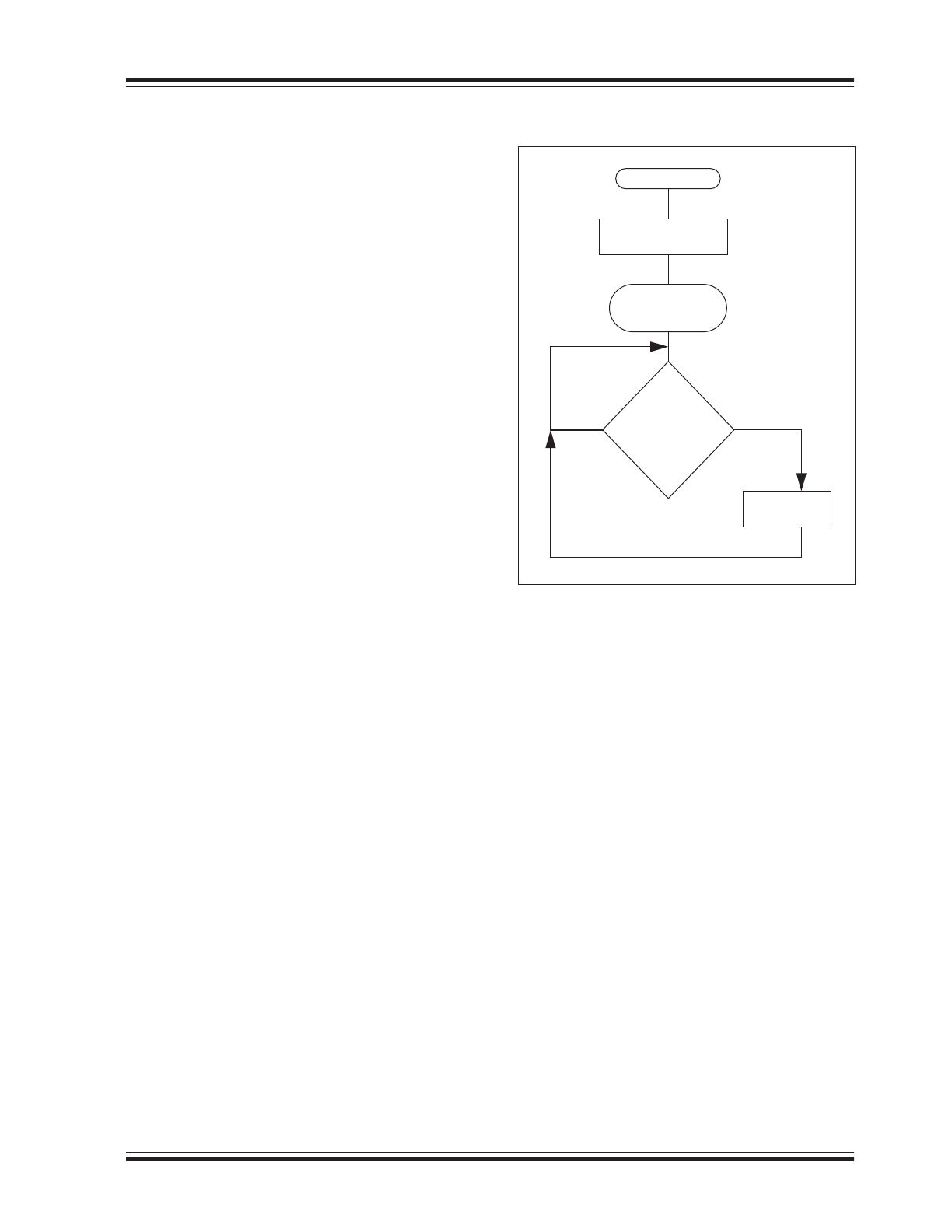
POWER-UP RESET DEVICE
CONFIGURATION BEHAVIOR
At Power-up Reset, the MCP2221 configures the
device options (GP designation, special function pins
parameters and USB enumeration options) according
to the Flash settings. Then, the Flash Chip Settings and
GP Settings are loaded into SRAM to allow for their
temporary modification at run time.
Chip Settings of the Device Configuration Flash are
copied partially into SRAM. Only the run-time-modifiable
parameters are copied into SRAM.
GP Settings of the Device Configuration Flash (GP
settings area) are copied entirely into the SRAM. By
copying the GP settings completely into SRAM, the
user is allowed to completely change the GP
designation at run time.
The SRAM copy of the settings can be altered at run
time in order to change certain device behavior, e.g.,
GP designation (the GPs can be re-assigned for a
different type of operation than the one assigned at
Power-up) and special parameters (DAC value,
ADC/DAC voltage references, Clock output value).
FIGURE 1-1:
CHIP SETTINGS RUN
TIME MANAGEMENT
The SRAM settings (GP and partial Chip Settings) can
be modified through USB HID commands and they will
have an effect on the following device features:
• GP pin designation (switch between GPIO,
dedicated or special functions modes)
• GPIO direction and output value (only for GPIO
outputs) – for the GPs assigned to work in GPIO
mode
• Clock Output duty cycle and value – if GP1 is
assigned for CLKR mode (Clock Reference
output mode), by modifying the SRAM settings,
the clock frequency and duty cycle can be
changed at run time
• DAC value and voltage reference used – the DAC
value setting as well as the voltage reference
used for it are stored in SRAM settings and they
can be changed at run time. Through this
mechanism, at run time the user can change the
DAC value, as well as the voltage reference.
• ADC voltage reference value – the voltage
reference used for ADC conversions can be
changed by altering its corresponding SRAM
setting
• Interrupt-on-change (IOC) detector settings – if
GP1 is assigned for IOC mode, the SRAM
settings are used for setting up the triggers used
for external interrupt detection (positive or
negative edge detection, or both)
Copy FLASH Chip and
GP settings to SRAM
USB enumeration
and configuration
complete
Change the
SRAM settings
Power-up Reset
changes needed
No Yes
SRAM settings

MCP2221
DS20005292C-page 6
2014-2017 Microchip Technology Inc.
1.4.2
CHIP SETTINGS MAP
The Chip Settings area resides in Flash memory and is
copied into SRAM at run time. Not all of the device’s
settings can be altered at run time. All the fields in the
Flash settings can be altered by the user.
TABLE 1-3:
CHIP SETTINGS MAP
Byte
Index
Register Name
Comments
0
CHIPSETTING0
Controls the USB CDC serial number enumeration, default state for the GP LED
designation, default state for GP dedicated-function pins and chip settings
protection level
1
CHIPSETTING1
Default clock output divider and duty cycle
2
CHIPSETTING2
DAC reference options and default DAC value
3
CHIPSETTING3
ADC reference and interrupt detection settings
4
USBVIDL
USB VID lower byte
5
USBVIDH
USB VID higher byte
6
USBPIDL
USB PID lower value
7
USBPIDH
USB PID higher byte
8
USBPWRATTR
USB power attributes
9
USBREQCRT
USB required current
10
PASS0
Password byte 0
11
PASS1
Password byte 1
12
PASS2
Password byte 2
13
PASS3
Password byte 3
14
PASS4
Password byte 4
15
PASS5
Password byte 5
16
PASS6
Password byte 6
17
PASS7
Password byte 7

2014-2017 Microchip Technology Inc.
DS20005292C-page 7
MCP2221
REGISTER 1-1:
CHIPSETTING0 REGISTER
R/W-0
R/W-1
R/W-1
R/W-1
R/W-1
R/W-1
R/W-0
R/W-0
CDCSNEN LEDURXINST LEDUTXINST LEDI2CINST SSPNDINST USBCFGINST CHIPPROT1 CHIPPROT0
bit 7
bit 0
Legend:
R = Readable bit
W = Writable bit
U = Unimplemented bit, read as ‘0’
-n = Value at POR
‘1’ = Bit is set
‘0’ = Bit is cleared
x = Bit is unknown
bit 7
CDCSNEN: USB CDC Serial Number Enable
1 = USB CDC Serial Number is enumerated
0 = No USB CDC Serial Number enumeration (factory default)
bit 6
LEDURXINST: LED UART R
X
Inactive State
1 = LED UART R
X
is inactive high and active low (factory default)
0 = LED UART R
X
is inactive low and active high
bit 5
LEDUTXINST: LED UART T
X
Inactive State
1 = LED UART T
X
is inactive high and active low (factory default)
0 = LED UART T
X
is inactive low and active high
bit 4
LEDI2CINST: LED I
2
C Inactive State
1 = LED I
2
C is inactive high and active low (factory default)
0 = LED I
2
C is inactive low and active high
bit 3
SSPNDINST: SSPND Inactive State
1 = SSPND is inactive high and active low (factory default)
0 = SSPND is inactive low and active high
bit 2
USBCFGINST: USBCFG Inactive State
1 = USBCFG is inactive high and active low (factory default)
0 = USBCFG is inactive low and active high
bit 1-0
CHIPPROT<1:0>: Chip Settings Protection Level
11 =Reserved
10 =Permanently locked
01 =Password protection
00 =Chip settings unprotected (factory default)
MCP2221
DS20005292C-page 8
2014-2017 Microchip Technology Inc.
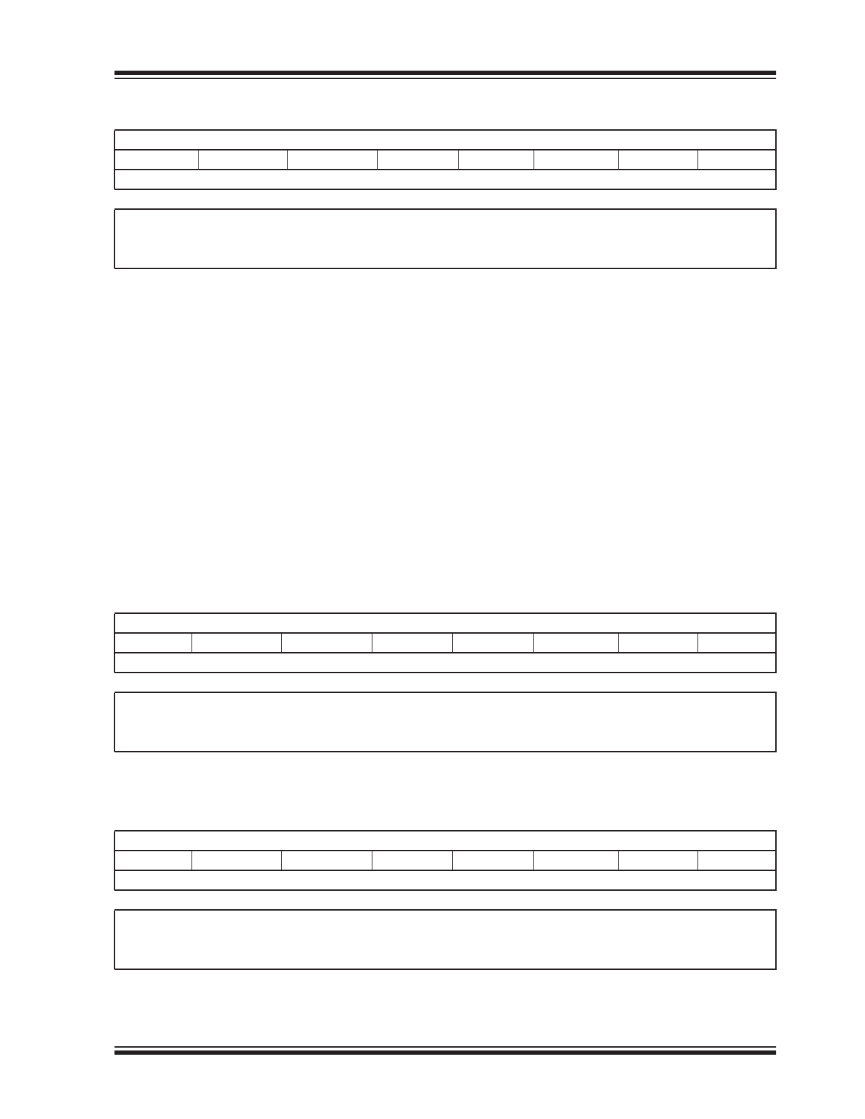
REGISTER 1-2:
CHIPSETTING1 REGISTER
R/W-0
R/W-0
R/W-0
R/W-1
R/W-0
R/W-0
R/W-1
R/W-0
—
—
—
CLKDC1
CLKDC0
CLKDIV2
CLKDIV1
CLKDIV0
bit 7
bit 0
Legend:
R = Readable bit
W = Writable bit
U = Unimplemented bit, read as ‘0’
-n = Value at POR
‘1’ = Bit is set
‘0’ = Bit is cleared
x = Bit is unknown
bit 7-5
Reserved: Set to ‘0’
bit 4-3
CLKDC<1:0>: Clock-Out Duty Cycle
11 =Duty cycle 75% (75% of 1 clock period is logic ‘1’ and 25% of 1 clock period is logic ‘0’)
10 =Duty cycle 50% (50% of 1 clock period is logic ‘1’ and 50% of 1 clock period is logic ‘0’)
(factory default)
01 =Duty cycle 25% (25% of 1 clock period is logic ‘1’ and 75% of 1 clock period is logic ‘0’)
00 =Duty cycle 0% (100% of 1 clock period is logic ‘0’)
bit 2-0
CLKDIV<2:0>: Clock-Out Divider Output
111 =375 kHz clock output
110 =750 kHz clock output
101 =1.5 MHz clock output
100 =3 MHz clock output
011 =6 MHz clock output
010 =12 MHz clock output (factory default)
001 =24 MHz clock output
000 =Reserved
REGISTER 1-3:
CHIPSETTING2 REGISTER
R/W-1
R/W-0
R/W-0
R/W-0
R/W-1
R/W-0
R/W-0
R/W-0
DACVRM1
DACVRM0
DACREF
DACVAL4
DACVAL3
DACVAL2
DACVAL1
DACVAL0
bit 7
bit 0
Legend:
R = Readable bit
W = Writable bit
U = Unimplemented bit, read as ‘0’
-n = Value at POR
‘1’ = Bit is set
‘0’ = Bit is cleared
x = Bit is unknown
bit 7-6
DACVRM<1:0>: DAC Internal Voltage Reference (DAC VRM) Selection
11 =VRM voltage is 4.096V (only if V
DD
is above this voltage)
10 =VRM voltage is 2.048V (factory default)
01 =VRM voltage is 1.024V
00 =VRM is off
bit 5
DACREF: DAC Reference Output Selection
1 = DAC reference output is DAC VRM voltage selection
0 = DAC reference output is V
DD
(factory default)
bit 4-0
DACVAL<4:0>: Initial DAC Output Value
5-bit value for the DAC output (factory default is 8 decimal)
2014-2017 Microchip Technology Inc.
DS20005292C-page 9
MCP2221
REGISTER 1-4:
CHIPSETTING3 REGISTER
R/W-0
R/W-1
R/W-1
R/W-0
R/W-1
R/W-1
R/W-0
R/W-0
—
INTDETFEEN INTDETREEN ADCVRM1
ADCVRM0
ADCREF
—
—
bit 7
bit 0
Legend:
R = Readable bit
W = Writable bit
U = Unimplemented bit, read as ‘0’
-n = Value at POR
‘1’ = Bit is set
‘0’ = Bit is cleared
x = Bit is unknown
bit 7
Reserved: Set to ‘0’
bit 6
INTDETFEEN: Interrupt Falling Edge Detect Enable
1 = Interrupt detector will trigger when a falling edge is detected (factory default)
0 = Falling edges will not trigger the detector
bit 5
INTDETREEN: Interrupt Rising Edge Detect Enable
1 = Interrupt detector will trigger when a rising edge is detected (factory default)
0 =
Rising edges will not trigger the detector
bit 4-3
ADCVRM<1:0>: ADC Internal Voltage Reference (ADC VRM) Selection
11 =VRM voltage is 4.096V (only if V
DD
is above this voltage)
10 =VRM voltage is 2.048V
01 =VRM voltage is 1.024V (factory default)
00 = VRM is off
bit 2
ADCREF: ADC Reference Output Selection
1 = ADC reference output is ADC VRM voltage selection (factory default)
0 =
ADC reference output is V
DD
bit 1-0
Reserved: Set to ‘0’
REGISTER 1-5:
USBVIDL REGISTER
R/W-1
R/W-1
R/W-0
R/W-1
R/W-1
R/W-0
R/W-0
R/W-0
USBVIDL7
USBVIDL6
USBVIDL5
USBVIDL4
USBVIDL3
USBVIDL2
USBVIDL1
USBVIDL0
bit 7
bit 0
Legend:
R = Readable bit
W = Writable bit
U = Unimplemented bit, read as ‘0’
-n = Value at POR
‘1’ = Bit is set
‘0’ = Bit is cleared
x = Bit is unknown
bit 7-0
USBVIDL<7:0>: USB VID Lower Byte (factory default: 0xD8(hex))
REGISTER 1-6:
USBVIDH REGISTER
R/W-0
R/W-0
R/W-0
R/W-0
R/W-0
R/W-1
R/W-0
R/W-0
USBVIDH7
USBVIDH6
USBVIDH5
USBVIDH4
USBVIDH3
USBVIDH2
USBVIDH1
USBVIDH0
bit 7
bit 0
Legend:
R = Readable bit
W = Writable bit
U = Unimplemented bit, read as ‘0’
-n = Value at POR
‘1’ = Bit is set
‘0’ = Bit is cleared
x = Bit is unknown
bit 7-0
USBVIDH<7:0>: USB VID Higher Byte (factory default: 0x04(hex))
MCP2221
DS20005292C-page 10
2014-2017 Microchip Technology Inc.
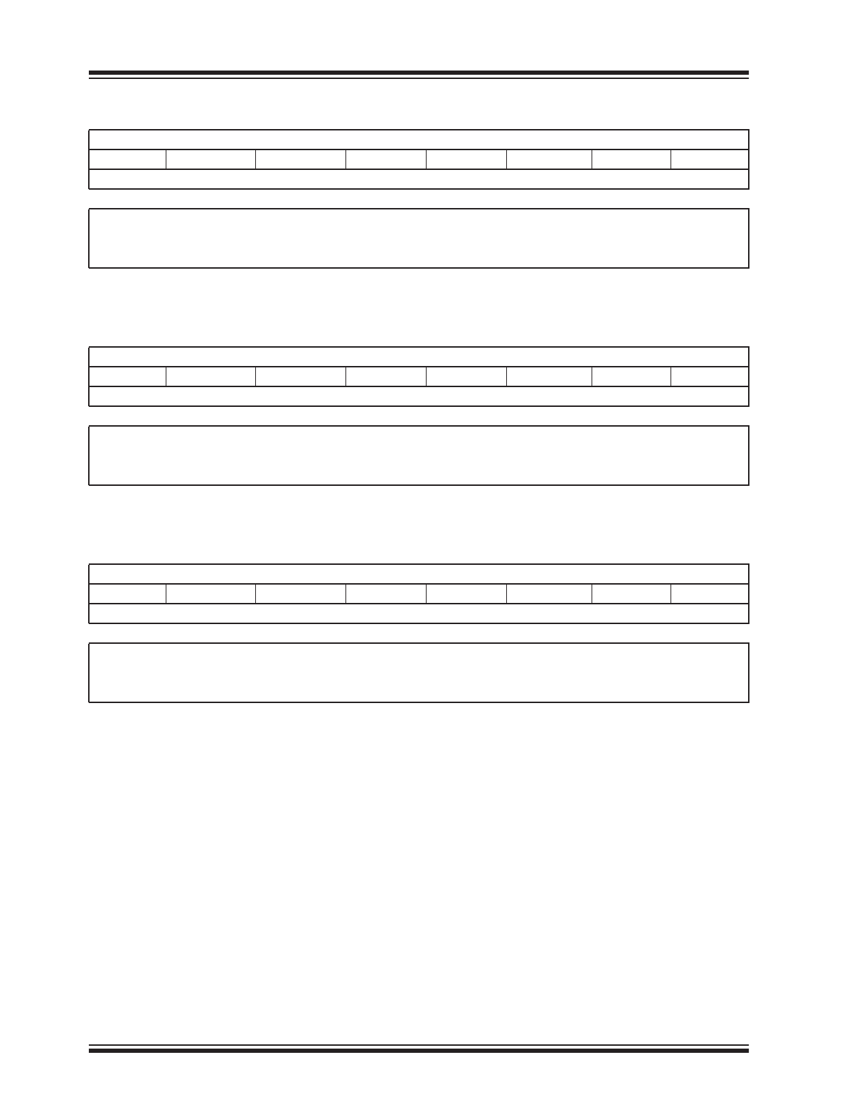
REGISTER 1-7:
USBPIDL REGISTER
R/W-1
R/W-1
R/W-0
R/W-1
R/W-1
R/W-1
R/W-0
R/W-1
USBPIDL7
USBPIDL6
USBPIDL5
USBPIDL4
USBPIDL3
USBPIDL2
USBPIDL1
USBPIDL0
bit 7
bit 0
Legend:
R = Readable bit
W = Writable bit
U = Unimplemented bit, read as ‘0’
-n = Value at POR
‘1’ = Bit is set
‘0’ = Bit is cleared
x = Bit is unknown
bit 7-0
USBPIDL<7:0>: USB PID Lower Byte (factory default: 0xDD(hex))
REGISTER 1-8:
USBPIDH REGISTER
R/W-0
R/W-0
R/W-0
R/W-0
R/W-0
R/W-0
R/W-0
R/W-0
USBPIDH7
USBPIDH6
USBPIDH5
USBPIDH4
USBPIDH3
USBPIDH2
USBPIDH1
USBPIDH0
bit 7
bit 0
Legend:
R = Readable bit
W = Writable bit
U = Unimplemented bit, read as ‘0’
-n = Value at POR
‘1’ = Bit is set
‘0’ = Bit is cleared
x = Bit is unknown
bit 7-0
USBPIDH<7:0>: USB PID Higher Byte (factory default: 0x00(hex))
REGISTER 1-9:
USBPWRATTR REGISTER
R/W-0
R/W-0
R/W-0
R/W-0
R/W-0
R/W-0
R/W-0
R/W-0
—
SELFPWR
REMWKUP
—
—
—
—
—
bit 7
bit 0
Legend:
R = Readable bit
W = Writable bit
U = Unimplemented bit, read as ‘0’
-n = Value at POR
‘1’ = Bit is set
‘0’ = Bit is cleared
x = Bit is unknown
bit 7
Reserved: Reserved – set to ‘1’ (factory default)
bit 6
SELFPWR: USB Self-Powered Attribute
1 = Chip will enumerate on the USB bus as being self-powered
0 = Chip will enumerate on the USB bus as being USB-bus powered (factory default)
bit 5
REMWKUP: USB Remote Wake-Up Capability
1 = Chip will enumerate on the USB bus as being able to wake-up the USB host
0 = Chip will enumerate as not being capable of remote wake-up of the USB host (factory default)
bit 4-0
Reserved: Set all bits to ‘0’ (factory default)