

2012-2014 Microchip Technology Inc.
DS20002299C-page 1
MCP2050
Features:
• The MCP2050 is compliant with:
- LIN Bus Specifications Version 1.3, 2.1 and
with SAE J2602-2
• Support Baud Rates Up to 20 kBaud
• 43V Load Dump Protected
• Maximum Continuous Input Voltage of 30V
• Wide LIN Compliant Supply Voltage, 6.0-18.0V
• Extended Temperature Range: -40 to +125°C
• Interface to PIC
®
EUSART and Standard USARTs
• Wake-Up on LIN Bus Activity or Local Wake Input
• LIN Bus Pin
- Internal pull-up termination resistor and diode
for slave node
- Protected against V
BAT
shorts
- Protected against loss of ground
- High current drive
• T
XD
and LIN Bus Dominant Time-Out Function
• Two Low-Power Modes
- Transmitter Off mode: 90 µA (typical)
- Power Down mode: 4.5 µA (typical)
• Output Indicating Internal Reset State (POR or
Sleep Wake)
• MCP2050 On-Chip Voltage Regulator
- Output voltage of 5.0V or 3.3V with 70 mA
capability and tolerances of ±3% over
operating temperature range
- Internal short-circuit current limit
- Only external filter and load capacitors needed
• Programmable Windowed Watchdog Timer
(WWDT)
- External resistor programmable from 7 ms to
140 ms
- Disabled by connecting the WWDTSELECT
pin to V
REG
or let the pin float
• Ratiometric Output of V
BAT
Voltage Scaled to
V
REG
• Automatic Thermal Shutdown
• High Electromagnetic Immunity (EMI), Low
Electromagnetic Emission (EME)
• Robust ESD Performance: ±15 kV for L
BUS
and
V
BB
pin (IEC61000-4-2)
• Transient Protection for L
BUS
and V
BB
Pins in
Automotive Environment (ISO7637)
• Meets Stringent Automotive Design Requirements
Including “OEM Hardware Requirements for LIN,
CAN and FlexRay Interfaces in Automotive
Applications”, Version 1.3, May 2012
• Multiple Package Options Including Small 5x5
QFN
Description:
The MCP2050 provides a bidirectional, half-duplex
communication physical interface to meet the LIN bus
specification Revision 2.1 and SAE J2602. The device
incorporates a voltage regulator with 5V or 3.3V 70 mA
regulated power supply output. The on-chip WWDT
allows users to adjust the size of the reset window by
using an external resistor. The ratiometric V
BAT
pin
scales down V
BAT
to the range of V
REG
so it can be
monitored by an A/D converter.
The device has been designed to meet the stringent
quiescent current requirements of the automotive
industry and will survive +4
3
V load dump transients,
and double battery jumps.
MCP2050 family members:
- MCP2050-500, 14-pin, LIN driver with 5.0V
regulator
- MCP2050-330, 14-pin, LIN driver with 3.3V
regulator
- MCP2050-500, 20-pin QFN, LIN driver with
5.0V regulator
- MCP2050-330, 20-pin QFN, LIN driver with
3.3V regulator
LIN Transceiver with Voltage Regulator
MCP2050
DS20002299C-page 2
2012-2014 Microchip Technology Inc.
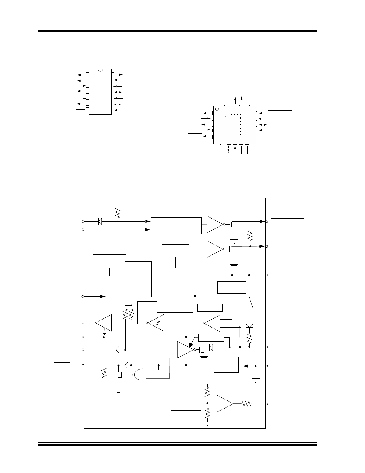
Package Types
Block Diagram
16
15
14
1
2
3
4
6
7
8
13
12
11
10
9
5
WWDTTRIG
FAULT/T
XE
V
BB
NC
V
BAT
RAT
IO
WWDT
R
E
SET
NC
CS/LWAKE
V
REG
T
XD
RXD
RESET
NC
V
SS
LBUS
17
18
19
20
NC
NC
NC
NC
WWDTSELECT
MCP2050
PDIP, SOIC
MCP2050
5 x 5 QFN*
EP
21
V
BAT
RATIO
R
XD
CS/LWAKE
V
REG
RESET
NC
WWDTRESET
WWDTTRIG
WWDTSELECT
FAULT/T
XE
V
BB
L
BUS
V
SS
1
2
3
4
14
13
12
11
10
9
8
5
6
7
T
XD
* Includes Exposed Thermal Pad (EP), see
Table 1-2
.
Voltage
Regulator
Ratiometric
Reference
Thermal
Protection
Internal Circuits
V
REG
FAULT/TXE
R
XD
T
XD
V
BB
L
BUS
V
SS
~30
CS/LWAKE
Wake-Up
Logic and
Power Control
RESET
Short-Circuit
Protection
Thermal
Protection
Programmable
Windowed Watchdog
WWDTRESET
WWDTTRIG
WWDTselect
V
BB
V
REG
V
BAT
RATIO
k
Ω
4.2V
Bus Wakeup
and
Short-Circuit
Slope Control
V
REG
4.2V
Bus
Dominant
Timer
300
Ω
V
REG
2012-2014 Microchip Technology Inc.
DS20002299C-page 3
MCP2050
1.0
FUNCTION DESCRIPTION
The MCP2050 provides a physical interface between a
microcontroller and a LIN half-duplex bus. It is intended
for automotive and industrial applications with serial
bus baud rates up to 20 kbaud. This device will
translate the CMOS/TTL logic levels to LIN logic levels,
and vice versa. The device offers optimum EMI and
ESD performance; it can withstand high voltage on the
LIN bus. The device supports two low-power modes to
meet automotive industry power consumption
requirements. The MCP2050 also provides a +5V or
3.3V 70 mA regulated power output.
1.1
Modes of Operation
The MCP2050 works in five modes: Power-On Reset
mode, Power-Down mode, Ready mode, Operation
mode, and Transmitter Off mode. For an overview of all
operational modes, please refer to
Table 1-1
. For the
operational mode transition, please refer to
Figure 1-1
.
FIGURE 1-1:
STATE DIAGRAM
POR
(2)
V
REG
OFF
RX OFF
TX OFF
READY
V
REG
ON
RX ON
TX OFF
TX OFF
V
REG
ON
RX ON
TX OFF
POWER-DOWN
V
REG
OFF
RX OFF
TX OFF
OPERATION
V
REG
ON
R
X
ON
T
X
ON
V
BB
> V
ON
CS/LWAKE =
1&
FAULT/TXE =
0
CS/LWAKE =
0
CS/LWAKE =
1 &
FAULT/T
XE
=
1
(3)
&
T
XD
=
1&
V
REG
_OK =
1
(1)
CS/LWAKE =
1&
FAULT/T
XE
=
1
(3)
&
T
XD
=
1
CS/LWAKE =
1&
FAULT/T
XE
=
0
CS/LWAKE =
0
CS/LWAKE =
1 OR
Voltage Rising Edge on LBUS
Note 1:
VREG_OK: Regulator Output Voltage > 0.8V
REG_NOM.
2:
If the voltage on pin V
BB
falls below V
OFF
, the device will enter Power-On Reset mode from all other
modes, which is not shown in the figure.
3:
FAULT/T
XE
= 1 represents input and no fault conditions. FAULT/T
XE
= 0 represents input low or a fault
condition. Refer to
Table 1-3
.

MCP2050
DS20002299C-page 4
2012-2014 Microchip Technology Inc.
1.1.1
POWER-ON-RESET MODE
Upon application of V
BB
, or whenever the voltage on
V
BB
is below the threshold of regulator turn-off voltage
V
OFF
(typically. 4.50V), the device enters Power-On
Reset mode (POR). During this mode, the device
maintains the digital section in a reset mode and waits
until the voltage on pin V
BB
rises above the threshold of
regulator turn-on voltage V
ON
(typically 5.75V) to enter
into Ready mode. In Power-On-Reset mode, the LIN
physical layer and voltage regulator are disabled, and
RESET output is forced to low.
1.1.2
READY MODE
The device enters Ready mode from POR mode after
the voltage on V
BB
rises above the threshold of
regulator turn-on voltage V
ON
or from Power-Down
mode when a remote or local wake-up event happens.
Upon entering Ready mode, the voltage regulator and
receiver section of the transceiver are powered up. The
transmitter remains in off state. The device is ready to
receive data but not to transmit. In order to minimize the
power consumption, the regulator operates in a
reduced-power mode. It has a lower GBW product and
thus is slower. However, the 70 mA drive capability is
unchanged.
The device stays in Ready mode until the output of the
voltage regulator has stabilized and the CS/LWAKE pin
is high (‘1’).
1.1.3
OPERATION MODE
If V
REG
is OK (V
REG
> 0.8 V
REG
_
NOM
), CS/LWAKE
pin, FAULT/T
XE
pin and T
XD
pin are high, the part
enters the Operation mode from either Ready or
Transmitter Off mode.
In this mode, all internal modules are operational. The
internal pull-up resistor between L
BUS
and V
BB
is
connected only in this mode.
The device goes into the Power-Down mode at the fall-
ing edge on CS/LWAKE; or to the Transmitter Off mode
at the falling on FAULT/T
XE
while CS/LWAKE stays high.
1.1.4
TRANSMITTER OFF MODE
In Transmitter Off mode, the receiver is enabled but the
L
BUS
transmitter is off. It is a lower-power mode.
In order to minimize the power consumption, the
window watchdog timer is disabled and the regulator
operates in a reduced-power mode. It has a lower
GBW product and thus is slower. However, the 70 mA
drive capability is unchanged.
The transmitter may be re-enabled whenever the
FAULT/T
XE
signal returns high, by removing the
internal fault condition and the CPU returning the
FAULT/T
XE
high. The transmitter will not be enabled
even if the FAULT/T
XE
pin is brought high externally,
when the internal fault is still present. However,
externally forcing the FAULT/T
XE
high, while the
internal fault is still present, should be avoided since
this will induce high current and power dissipation in
the FAULT/T
XE
pin.
The transmitter is also turned off whenever the voltage
regulator is unstable or recovering from a fault. This
prevents unwanted disruption of the bus during times of
uncertain operation.
1.1.5
POWER-DOWN MODE
In Power-Down mode, the transceiver and the voltage
regulator are both off. Only the Bus Wake-up section
and the CS/LWAKE pin wake-up circuits are in opera-
tion. This is the lowest-power mode.
If any bus activity (e.g. a BREAK character) occurs
during Power-Down mode, the device will immediately
enter Ready mode and enable the voltage regulator.
Then, once the regulator output has stabilized (approx-
imately 0.3 ms to 1.2 ms) it goes to Operation mode.
Refer to
Section
1.1.6 “Remote Wake-up”
for more
details.
The part will also enter Ready mode from Power-Down
mode, followed by Operation mode, if the CS/LWAKE
pin becomes active high (‘1’).
1.1.6
REMOTE WAKE-UP
The remote wake-up sub module observes the L
BUS
in
order to detect bus activity. In Power-Down mode, nor-
mal LIN recessive/dominant threshold is disabled, and
the LIN bus Wake-Up Voltage Threshold V
WK(LBUS)
is
used to detect bus activities. Bus activity is detected
when the voltage on the L
BUS
falls below the LIN bus
Wake-Up Voltage Threshold V
WK(LBUS)
(approximately
3.4V) for at least t
BDB
(a typical duration of 80 µs) fol-
lowed by a rising edge. Such a condition causes the
device to leave Power-Down mode
2012-2014 Microchip Technology Inc.
DS20002299C-page 5
MCP2050
.
1.2
Windowed Watchdog Reset
The Watchdog Timer monitors for activity on the
Windowed Watchdog Timer Trigger input pin
WWDTTRIG. The WWDTTRIG pin is expected to be
strobed within a given time frame. When this time frame
has expired without an edge transition on the WWDTTRIG
pin, the WWDTRESET pin is driven active (low) to reset
the system. This feature is enabled by connecting a
resistor between the WWDTSELECT pin and V
SS
.
Monitoring is then done by requiring the host processor to
force a falling edge transition on the WWDTTRIG pin
within a predetermined time frame (T
WD
).
The start time of the trigger window is fixed at 50% of
the total watchdog period, after the last trigger. The
length of the window is determined by the value of the
resistor on pin WWDTSELECT. The Watchdog Timer is
disabled if WWDTSELECT is floating.
1.2.1
WWDT DURING INITIAL POWER-UP
The WWDTRESET is driven high after a power-on
reset. The Watchdog Timer begins counting at this
point, awaiting an edge on WWDTTRIG pin. Note that
there is no window enabled, yet. If no falling edge is
detected on the WWDTTRIG pin before the timer
expires, the WWDTRESET is pulse low and the timer
is restarted. When a trigger edge on the WWDTTRIG
pin is seen, the window is enabled and the timer is reset.
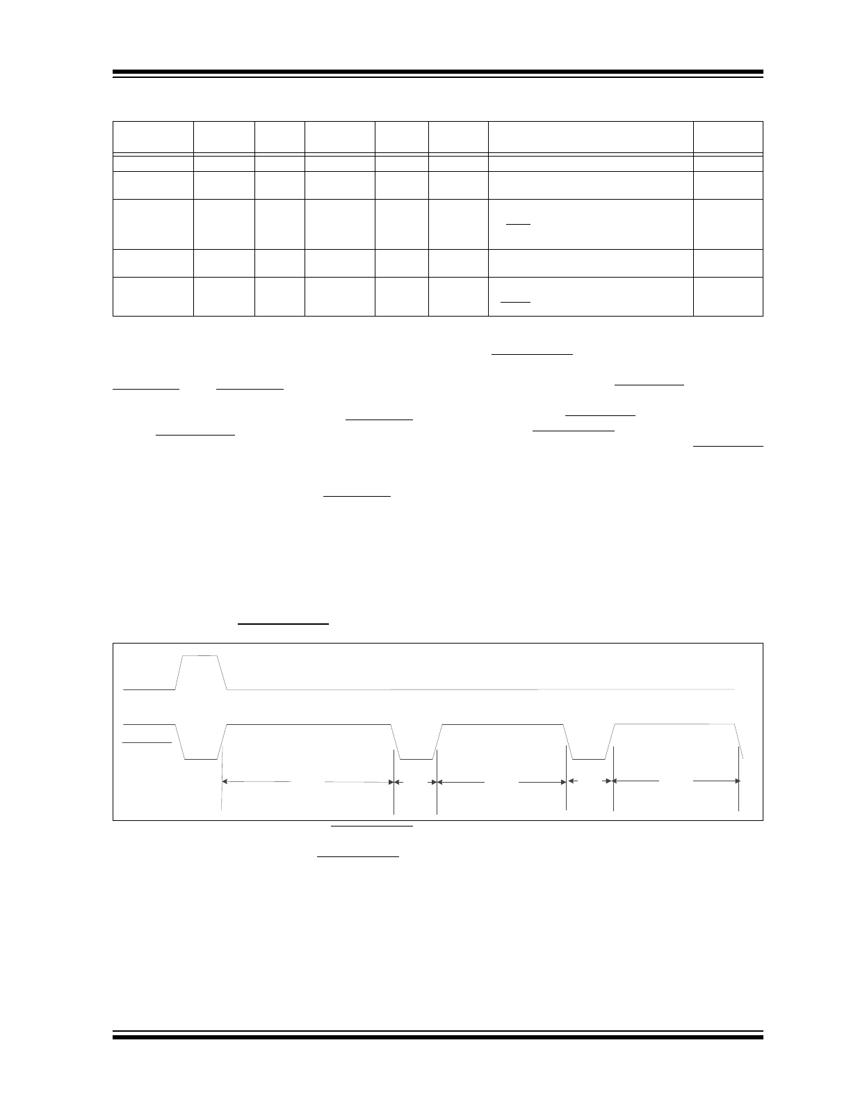
FIGURE 1-2:
WWDTRESET DURING INITIAL POWER-UP
Figure 1-2
shows the behavior of the WWDTRESET
pin after a system reset with no trig at all. If no trig is
given during the power-up window, WWDTRESET is
reset low for the time t
WDRST
.
The power-up window length t
POWERUP
duration is
determined by the value of the resistor connected
between pin WWDTSELECT and pin V
SS
, while the
reset pulse duration is about 150 μs.
Duration for t
POWERUP
and t
WDRST
are:
• t
POWERUP
= 0.8 ms x (R
WWDTSELECT
+1) typical
• t
WDRST
= 150 μs typical
• R
WWDTSELECT
is in kΩ
Once a trig is asserted, the power-up sequence “stops”
and the normal behavior begins.
TABLE 1-1:
OVERVIEW OF OPERATIONAL MODES
State
Transmitter Receiver
Internal
Wake Module
Voltage
Regulator
Watch Dog
Timer
Operation
Comments
PoR
Off
Off
Off
Off
Off
Proceed to Ready mode after V
BB
>V
ON
.
—
Ready
Off
On
Off
On
On
If CS/LWAKE high, then proceed to Operation
or Transmitter Off mode.
Bus Off state
Operation
On
On
Off
On
On
If CS/LWAKE low level, then proceed to
Power-Down.
If FAULT/T
XE
low level, then Transmitter-Off
mode.
Normal
Operation
mode
Power-Down
Off
Off
On
Activity Detect
Off
Off
On LIN bus rising edge or CS/LWAKE high
level, proceed to READY mode.
Lowest-
Power mode
Transmitter Off
Off
On
Off
On
Off
If CS/LWAKE low level, then proceed to
Power down.
If FAULT/T
XE
high, then Operation mode.
Bus Off state,
Lower-Power
mode
t
POWERUP
t
WDRST
t
POWERUP
Internal
reset
WWDTRESET
t
POWERUP
t
WDRST
MCP2050
DS20002299C-page 6
2012-2014 Microchip Technology Inc.
1.2.2
WINDOWED WATCHDOG
BEHAVIOR
After windowed watchdog begins its normal behavior,
three different cases can appear.
• A pulse (falling edge) on the WWDTTRIG pin is
detected within the trigger window; the watchdog
timer will be reset, and a new watchdog period will
begin; WWDTRESET pin remains high (
Figure 1-3
.)
• A pulse (falling edge) on the WWDTTRIG pin is
detected before the trigger window (too early trig-
ger); WWDTRESET is asserted (low) immediately
after the falling edge is detected for approximately
t
WDRST
; the counter is reset and the next watchdog
period begins at the rising edge of the voltage on
WWDTRESET pin (
Figure 1-12
).
• No pulse on the WWDTTRIG pin is detected
during the whole watchdog window (no trigger);
WWDTRESET is asserted (low) for approximately
t
WDRST
when the timer has expired; the counter is
reset and the next watchdog period begins at the
rising edge of the voltage on WWDTRESET pin
(
Figure 1-5
).
The trigger window is between 50% to 100% of the
watchdog window length, t
WLENGTH
. The window
length is determined by the external resistor between
WWDTSELECT pin and V
SS
.
EQUATION 1-1:
t
WDRST
= 150 μs typical
R
WWDTSELECT
is in kΩ; its value ranges from 33 kΩ to
680 kΩ and window length ranges from 7 ms to 120 ms
typical.
If the WWDTSELECT pin is floating, the watchdog is
disabled and the WWDTRESET remains high.
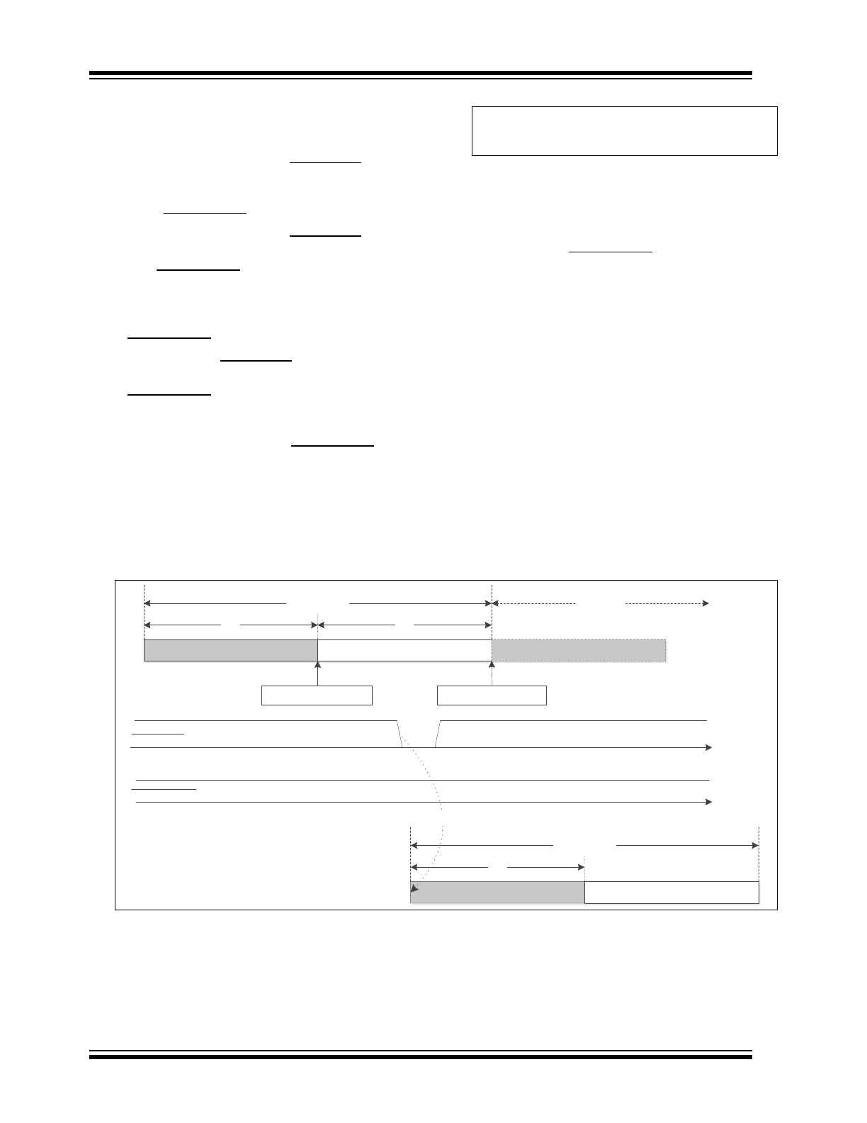
FIGURE 1-3:
CORRECT TRIGGER
t
WLENGTH
= (0.175 ms × RWWDTSELECT) + 1.2 typical
Too early
Trigger window
Window length
50%
Earliest trigger point
Lastest trigger point
Next period
Too early
Trigger window
Window length
50%
New period begins
WWDTTRIG
WWDTRESET
1
0
1
T
WD
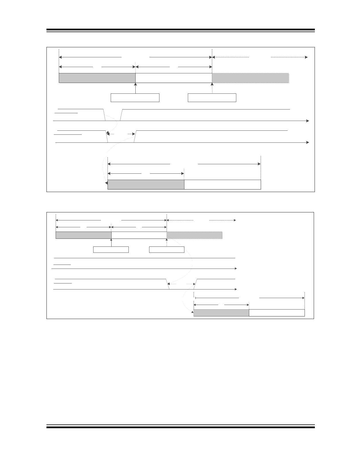
2012-2014 Microchip Technology Inc.
DS20002299C-page 7
MCP2050
FIGURE 1-4:
TOO EARLY TRIGGER
FIGURE 1-5:
NO TRIGGER
Too early
Trigger window
Window length
50%
Earliest trigger point
Lastest trigger point
Next period
Too early
Trigger window
Window length
50%
New period begins
WWDTTRIG
WWDTRESET
1
0
1
0
T
WD
t
WDRST
Too early
Trigger window
Window length
50%
Earliest trigger point
Lastest trigger point
Next period
Too early
Trigger window
Window length
50%
New period begins
WWDTTRIG
WWDTRESE
T
1
0
1
T
WD
No trigger, timer expired
t
WDRST
MCP2050
DS20002299C-page 8
2012-2014 Microchip Technology Inc.
1.3
Pin Descriptions
Please refer to
Table 1-2
for the pinout overview.
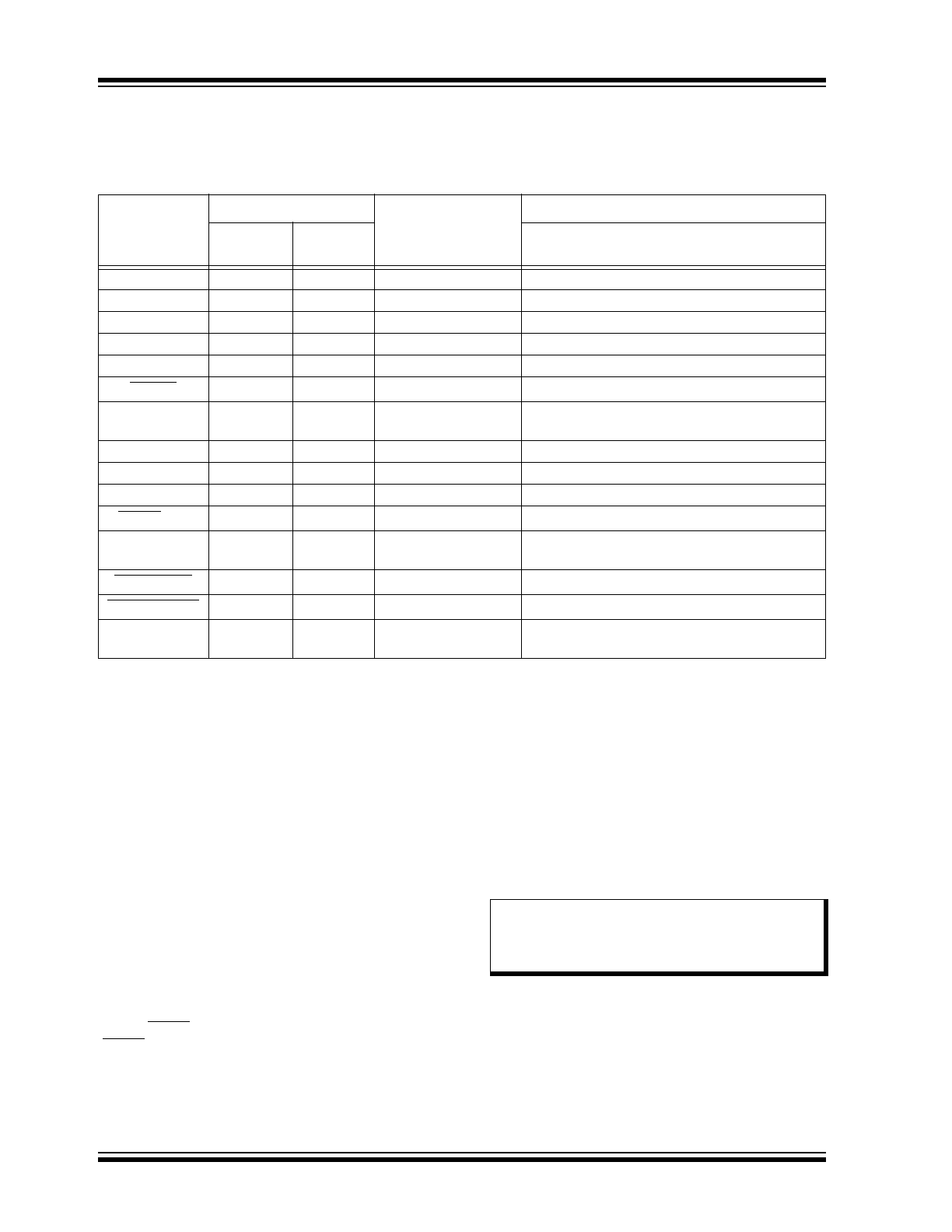
TABLE 1-2:
PINOUT DESCRIPTIONS
1.3.1
V
BAT
RATIO
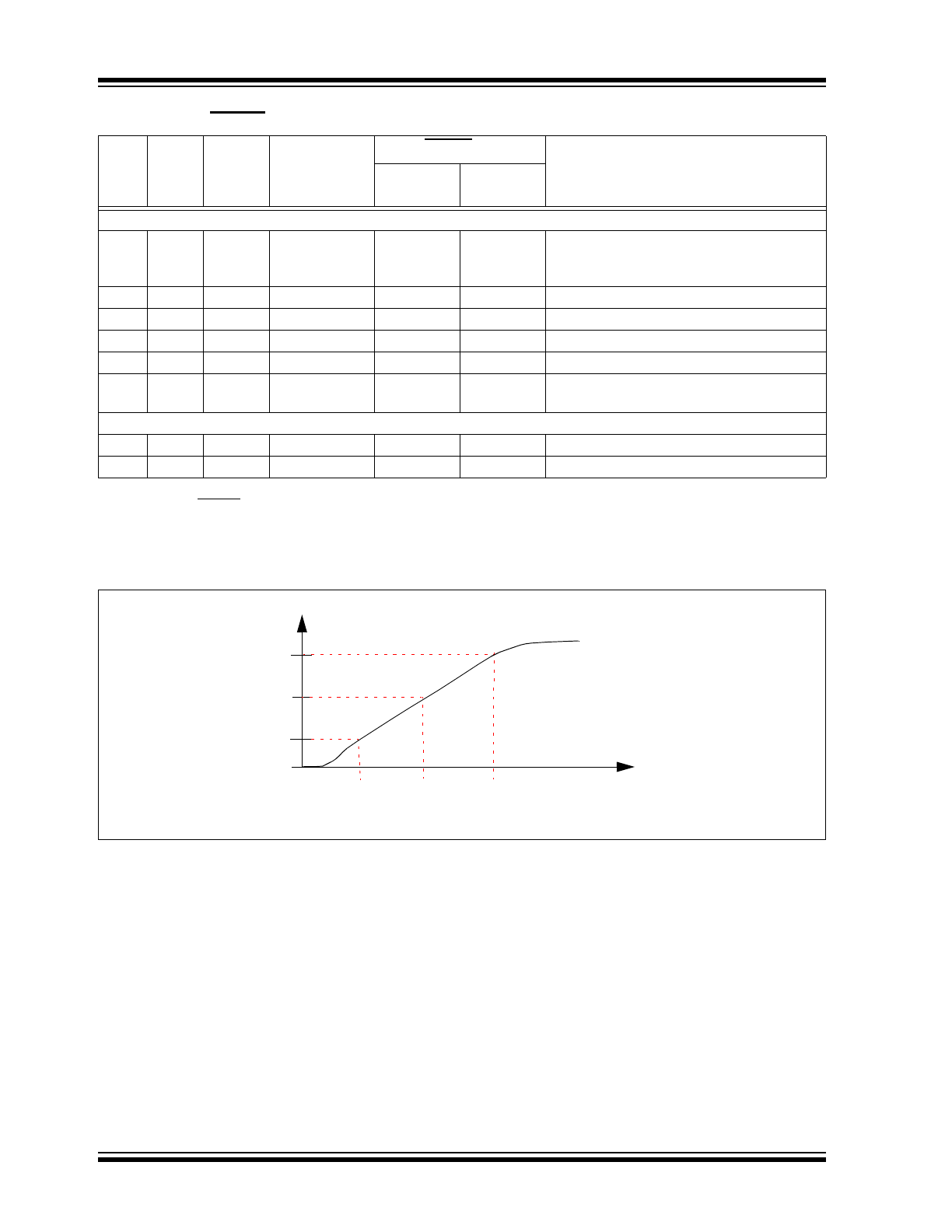
This is an analog output pin that reflects the voltage at
the
V
BAT
pin. It is scaled by
V
REG
such that:
V
BAT
RATIO = V
BAT
/24 × V
REG
0 <= V
BAT
RATIO <= V
REG
The resistive divider and the output driver are switched
off during Power-Down mode in order to reduce power
consumption.
1.3.2
R
XD
Receive Data Output pin. The R
XD
pin is a standard
CMOS output pin and it follows the state of the LBUS pin.
1.3.3
CS/LWAKE
Chip Select and Local Wake-Up Input pin (TTL level,
high voltage tolerant). This pin controls the device state
transition. Refer to
Figure 1-1
.
If CS/LWAKE = 1, the device can work in Operation
mode (FAULT/T
XE
= 1) or Transmitter Off mode
(FAULT/T
XE
= 0).
If CS/LWAKE = 0, the device can work in Power-Down
mode or Ready mode.
An internal pull-down resistor will keep the CS/LWAKE
pin low to ensure that no disruptive data will be present
on the bus while the microcontroller is executing a
Power-on Reset and I/O initialization sequence. When
CS/LWAKE is ‘1’, a weak pull-down (~600 kΩ) is used
to reduce current. When CS/LWAKE is ‘0’ a stronger
pull-down (~300 kΩ) is used to maintain the logic level.
This pin may also be used as a local wake-up input
(see
Figure 1-12
). The microcontroller will set the I/O
pin to control the CS/LWAKE. An external switch, or
other source, can then wake-up both the transceiver
and the microcontroller.
PIN Name
Devices
PIN Type
Function
14-Pin
PDIP, SOIC
5 x 5 QFN
Normal Operation
V
BAT
RATIO
1
18
Analog Output
V
BAT
RATIO = V
BAT
/24 × V
REG
R
XD
2
1
Output
Receive Data Output
CS/LWAKE
3
2
TTL Input, HV-tolerant Chip Select and Local Wake-up Input
V
REG
4
3
Output
Voltage Regulator Output
T
XD
5
4
Input, HV-tolerant
Transmit Data Input
RESET
6
5
Output
Reset Output
NC
7
6,9,10,11,
16,19,20
Not Connected
—
V
SS
8
8
Power
Ground
L
BUS
9
7
I/O, HV
LIN Bus
V
BB
10
12
Power
Battery
FAULT/T
XE
11
13
I/O, HV-tolerant
Fault Detect Output/Transmitter Enable Input
WWDTSELECT
12
14
Input
A Resistor between this pin and Ground
determines the Watchdog Window length
WWDTTRIG
13
15
Input
Windowed Watchdog Trigger Input
WWDTRESET
14
17
Output, HV-tolerant
Windowed Watchdog Reset Output
EP
—
21
Exposed Thermal Pad
(EP)
Exposed Thermal Pad can be left unconnected,
or connected to the ground.
Note:
CS/LWAKE should NOT be tied directly to
pin V
REG
as this could force the
MCP2050 into Operation Mode before the
microcontroller is initialized.

2012-2014 Microchip Technology Inc.
DS20002299C-page 9
MCP2050
1.3.4
V
REG
Positive Supply Voltage Regulator Output pin. An on-
chip LDO gives +5.0 or +3.3V 70 mA regulated voltage
on this pin.
1.3.5
T
XD
Transmit Data Input pin (TTL level, HV compliant,
adaptive pull-up). The transmitter reads the data
stream on T
XD
pin and sends it to LIN bus. The LBUS
pin is low (dominant) when T
XD
is low, and high
(recessive) when T
XD
is high.
The Transmit Data Input pin has an internal adaptive
pull-up to an internally-generated 4.2V (approximate).
When T
XD
is ‘0’, a weak pull-up (~900 kΩ) is used to
reduce current. When T
XD
is ‘1’ a stronger pull-up
(~300 kΩ) is used to maintain the logic level. A series
reverse-blocking diode allows applying T
XD
input
voltages greater than the internally generated 4.2V and
renders T
XD
pin HV compliant up to 30V (see the Block
Diagram on page 2).
1.3.6
RESET
Reset Output pin. This pin is open drain with ~90 kΩ
pull-up to V
REG
. It indicates the internal voltage has
reached a valid, stable level. As long as the internal
voltage is valid (above 0.8V
REG
), this pin will remain
high (‘1’); otherwise the RESET pin switches to low (‘0’).
1.3.7
V
SS
Ground pin.
1.3.8
L
BUS
L
BUS
is a bidirectional LIN bus Interface pin and is
controlled by the signal T
XD
. It has an open collector
output with a current limitation. To reduce
electromagnetic emission, the slopes during signal
changes are controlled, and the L
BUS
pin has
corner-rounding control for both falling and rising edges.
The internal LIN receiver observes the activities on LIN
bus, and generates the output signal R
XD
that follows
the state of the L
BUS
. A first degree 160 kHz, low-pass
input filter optimizes electromagnetic immunity.
1.3.9
V
BB
Battery Positive Supply Voltage pin. An external diode
is connected in series to prevent the device from being
reversely powered (refer
Figure 1-12
).
1.3.10
FAULT/TXE
Fault Detect Output/Transmitter Enable Input pin. The
output section is HV tolerant open drain (up to 30V).
The input section is identical with T
XD
section (TTL
level, HV compliant, adaptive pull-up). The internal pull-
up resistor may be too weak for some applications. An
external 10kΩ pull-up resistor is recommended to
ensure a logic high level. Its state is defined as shown
in
Table 1-3
. The device is placed in Transmitter Off
mode whenever this pin is low (‘0’), either from an
internal fault condition or by external drive.
If CS/LWAKE is high (‘1’), the FAULT/T
XE
signals a mis-
match between the T
XD
input and the L
BUS
level. This
can be used to detect a bus contention. Since the bus
exhibits a propagation delay, the sampling of the inter-
nal compare is debounced to eliminate false faults.
After the device wakes up, the FAULT/T
XE
indicates
what wakes the device if CS/LWAKE remains low (‘0’)
(refer to
Table 1-3
).
The FAULT/T
XE
pin sampled at a rate faster than every
10 µs.
1.3.11
WWDTSELECT
This is an analog input pin that sets the open window
time to accept a trigger reset. A resistor between this
pin and V
SS
sets this time. The equation to determine
the value of the resistor can be found in
Section 1.2.2
“Windowed Watchdog Behavior”
.
1.3.12
WWDTTRIG
This is an input pin to reset the Windowed Watchdog
Timer. A high-to-low transition during the open window
time will reset the timer and prevent the WWDT from
timing out. The pin has an internal adaptive pull-up to
an internally-generated 4.2V (approximate.).
When WWDTTRIG is ‘0’, a weak pull-up (~800 kΩ
is
connected
to reduce current.
When WWDTTRIG is ‘1’, the pull-up is stronger to
maintain the logic level.
1.3.13
WWDTRESET
WWDTRESET is an open-drain output pin. This pin is
asserted low when the internal Windowed Watchdog
Timer has expired or an attempt was made to clear the
timer before the window has opened.
1.3.14
EP
It is recommended to connect this pad to V
SS
to enhance
electromagnetic immunity and thermal resistance.
MCP2050
DS20002299C-page 10
2012-2014 Microchip Technology Inc.
FIGURE 1-6:
V
BAT
RATIO OUTPUT RANGE
TABLE 1-3:
FAULT/TXE TRUTH TABLE
T
XD
In
R
XD
Out
LIN
BUS
I/O
Thermal
Override
FAULT/T
XE
Definition
External
Input
Driven
Output
CS = 1
L
H
V
BB
OFF
H
L
FAULT
, T
XD
driven low, L
BUS
shorted to V
BB
(Note 1)
,
or L
BUS
/T
XD
permanent dominant
detected, and transmit time-out shutdown.
H
H
V
BB
OFF
H
H
OK
L
L
GND
OFF
H
H
OK
H
L
GND
OFF
H
H
OK
, data is being received from L
BUS
x
x
V
BB
ON
H
L
FAULT
, transceiver in thermal shutdown
x
x
V
BB
x
L
x
NO FAULT
, the CPU is commanding the
transceiver to turn off the transmitter driver
CS = 0 after a wake-up
x
x
x
x
x
L
Wake-up from LIN bus activity
x
x
x
x
x
H
Wake-up from POR
Legend:
x = don’t care
Note 1:
The FAULT/T
XE
is valid after approximately 25 µs after T
XD
falling edge. This is to eliminate false fault
reporting during bus propagation delays.
Note 1:
Linear range of V
BAT
RATIO is between V
BB
= 6.0-18.0V.
0
V
BB
.25V
REG
.75V
REG
V
REG
/2
V
BAT
RATIO
6V
12V
18V
24V