
© 2009 Microchip Technology Inc.
DS22186C-page 1
MCP2036
Features:
• Complete Inductance Measurement System:
- Low-Impedance Current Driver
- Sensor/Reference Coil Multiplexer
- High-Frequency Detector
• Operating Voltage: 2.7 to 5.5V
• Low-Power Standby Mode
• Gain and Frequency set by external passive
components
Typical Applications:
• Harsh environment inductive keyboards
• Inductive rotational sensor interface
• Inductive displacement sensor interface
• Inductive force sensor interface
Description:
The MCP2036 Inductive Sensor Analog Front End
(AFE) combines all the necessary analog functions for
a complete inductance measurement system.
The device includes:
• High-frequency, current-mode coil driver for
exciting the sensor coil.
• Synchronous detector for converting AC sense
voltages into DC levels.
• Output amplifier/filter to improve resolution and
limit noise.
• Virtual ground reference generator for single
supply operation.
The device is available in 14-pin PDIP, SOIC and
16-pin QFN packages:
Package Types
1
2
3
6
7
4
5
14
13
8
9
10
11
12
V
REF
LREF
LBTN
V
DD
DRVOUT
DRVIN
CLK
V
DET+
V
DET-
V
DETOUT
V
SS
CS
REFSEL
ISOL
9
10
11
12
6
7
5
8
1
2
3
4
LREF
LBTN
V
DD
DRVOUT
16
15
14
13
DR
VIN
CL
K
REF
SEL
CS
V
DET-
V
DETOUT
V
SS
ISOL
V
DE
T
+
V
RE
F
NC
NC
MCP2036
16-pin QFN
MCP2036
14-pin PDIP, SOIC
Inductive Sensor Analog Front End Device
MCP2036
DS22186C-page 2
© 2009 Microchip Technology Inc.
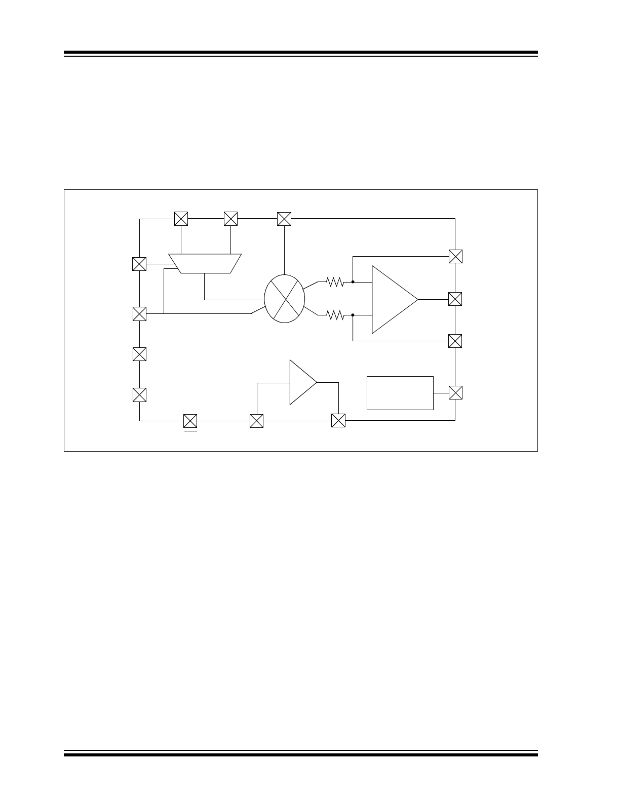
1.0
FUNCTIONAL DESCRIPTION
The MCP2036 measures a sensor coil’s impedance by
exciting the coil with a pulsed DC current and
measuring the amplitude of the resulting AC voltage
waveform. The drive current is generated by the
on-chip current amplifier/driver which takes the
high-frequency triangular waveform present on the
DRVIN input, and amplifies it into the pulsed DC current
for exciting the series combination of the sensor coils.
The AC voltages generated across the coils, are then
capacitively coupled into the LBTN and LREF inputs.
An input resistance of 2K between the inputs and the
virtual ground offsets the AC input voltages up to the
signal ground generated by the reference voltage
generator, as shown in
Figure 1-1
.
FIGURE 1-1:
MCP2036 Block Diagram
Voltage
Reference
REFSEL
V
DETOUT
DRVIN
CLK
DRVOUT
LBTN
LREF
V
REF
V
DD
V
SS
0
1
Input MUX
CS
Key Inductor Driver
Mixer
V
DET+
V
DET-
+
-
10K
10K
Op. Amp. Block
ISOL
© 2009 Microchip Technology Inc.
DS22186C-page 3
MCP2036
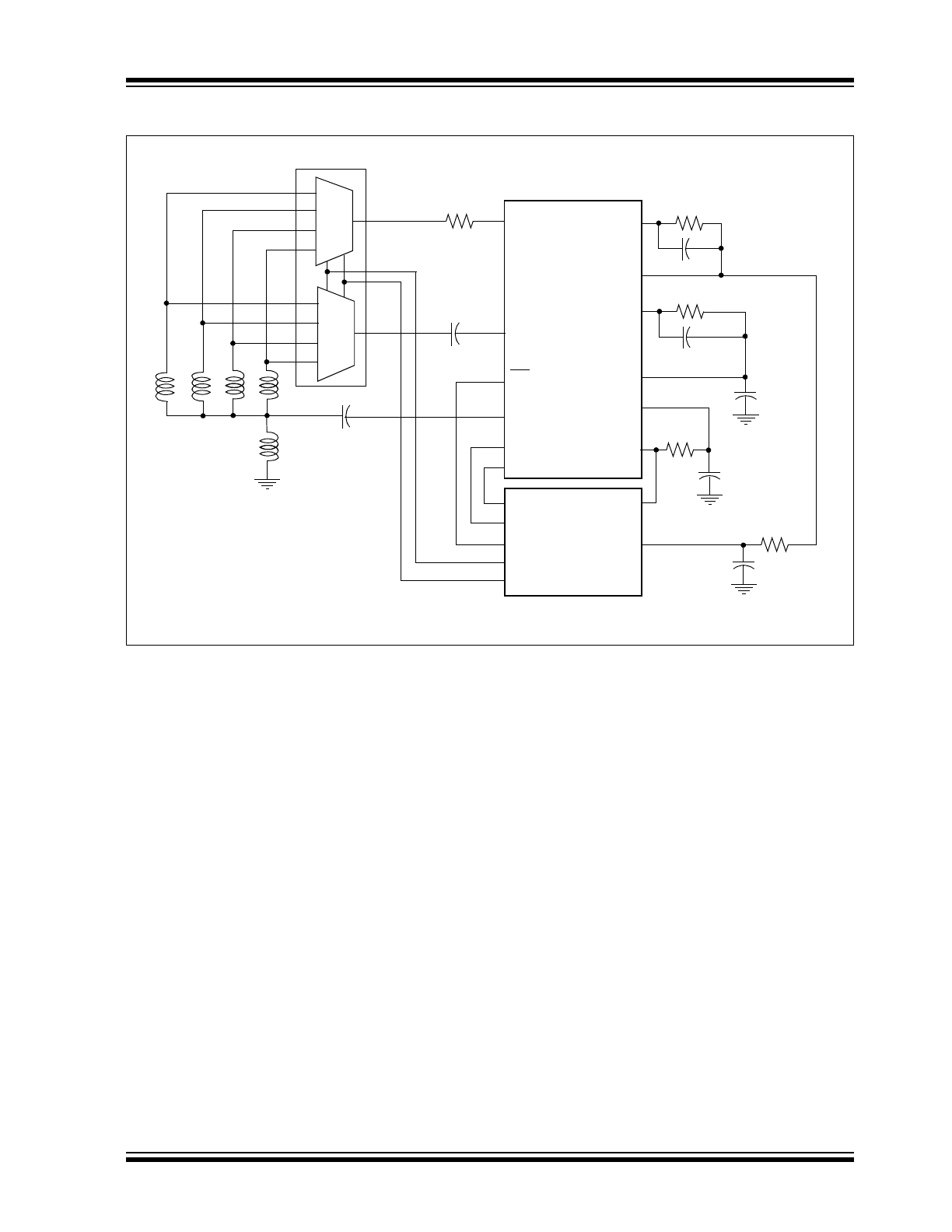
FIGURE 1-2:
MCP2036 Typical Application
The coil voltages are then multiplexed into the
Synchronous Detector section by the LBTN/LREF
multiplexer. This allows the microcontroller to select
which signal is sampled by the detector. The detector
converts the coil voltages into a DC level using a
frequency mixer, amplifier, and filter.
The mixer is composed of two switches driven by the
clock present on the CLK signal input. The switches
toggle the amplifier/filter between an inverting and
non-inverting topology, at a rate equal to the clock input
frequency. This inverts and amplifies the negative side
of the signal, while amplifying the positive side. The
result is a pulsed DC signal with a peak voltage,
proportional to the amplitude of the AC coil voltage.
The gain of the detector is set by two pairs of resistors;
one pair are the internal fixed series resistors between
the frequency mixer and the amplifier. The second
resistor pair are the two external gain set resistors
(R
GAIN
). The two capacitors (C
FILTER
) in parallel with
the external gain setting resistors form a low pass filter
which converts the pulsed DC output signal into a
smooth DC voltage which is proportional to the AC
sensor voltage input. The output of the system is
present on the V
DETOUT
pin, which drives the
microcontroller’s ADC input for conversion into a digital
value.
The virtual ground reference for the detector/amplifier
is generated by a second internal op amp which
produces a virtual ground equal to ½ the supply
voltage. The virtual ground is available externally at the
V
REF
output and used internally throughout the
detector circuit, allowing single supply operation. A
small external capacitance is required to stabilize this
output and limit noise.
The ISOL input is used to isolate the detector from
potential noise sources during the measurement of the
virtual ground reference during a button measurement.
MCP2036
LREF
LBTN
LREF
DRVOUT
10
Ω
10nF
REFSEL
10nF
I/O
I/O
I/O
0
1
2
3
0
1
3
2
CD4052
Key Coils
PIC
®
Microcontroller
CS
I/O
V
DET-
V
DETOUT
V
DET+
V
REF
CLK
DRVIN
PWM
ADC
C
FILTER
C
FILTER
R
GAIN
R
GAIN
C
RGND
R
IN
C
IN
R
ADC
C
ADC
ISOL
I/O

MCP2036
DS22186C-page 4
© 2009 Microchip Technology Inc.
1.1
Coil Driver
The coil driver produces the excitation current for the
sensor coils.
The coil driver input is derived from the digital clock
supplied to the CLK input. The digital signal is first
filtered through a low-pass filter, composed of R
IN
and
C
IN
, and passed to the DRVIN input. The driver will
create a triangular current in phase and proportional
with the input voltage. Because the digital drive into the
R
IN
-C
IN
filter has a 50% duty cycle, the voltage on the
DRVIN input will be centered at V
DD
/2. The relationship
between voltage, current, inductance and frequency is
shown in
Equation 1-1
.
EQUATION 1-1:
1.2
Synchronous Detector and Output
Amplifier
The Synchronous Detector has two inputs, LREF and
LBTN, selectable by REFSEL. This routes either signal
into the frequency mixer of the detector. The frequency
mixer then converts the AC waveform into a pulsed DC
signal which is amplified and filtered.
The gain of the amplifier is user-settable, using an
external resistor, R
GAIN
(see
Equation 1-2
).
EQUATION 1-2:
An ADC plus firmware algorithm then digitizes the
detector output voltage and uses the resulting data to
detect a key press event.
1.3
Virtual Ground Voltage Reference
Circuit
To create both an inverting and non-inverting amplifier
topology, a pseudo split supply design is required. To
generate the dual supplies required, a rail splitter is
included, which generates the virtual ground by creat-
ing a voltage output at V
DD
/2. The output is used by the
external passive network of the Detector/Amplifier sec-
tion as a reference on the non-inverting input. A bypass
capacitor of 0.1 uF is required to ensure the stability of
the output. For reference accuracy, no more than 3 mA
should be supplied to, or drawn from the reference
output pin.
ΔV
OUT
ΔI
DRV
L
COIL
•
2
F
DRV
•
•
(
)
=
V
OUT
Pulsed Output Voltage
=
ΔI
DR V
AC Drive Current Amplitude
=
F
DRV
AC Drive Current Frequency
=
L
COIL
Inductance of the Sensor Coil
=
Note:
These equations assume a 50% duty cycle.
Note:
The output amplifier/filter uses a
differential connection, so its output is
centered to V
REF
(V
DD
/2). The amplitude
of the detected signal should be calculated
as the difference between voltages at the
output of the detector and the reference
voltage.
Gain
R
GAIN
10kOhm
⁄
∼
© 2009 Microchip Technology Inc.
DS22186C-page 5
MCP2036
2.0
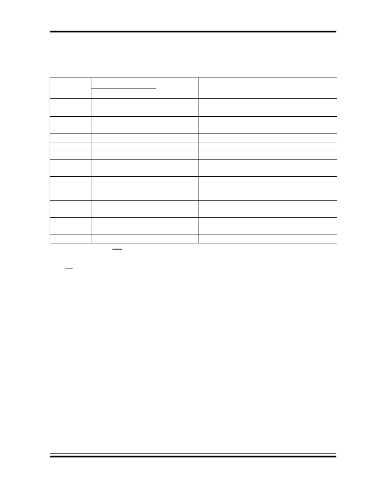
PIN DESCRIPTION
Descriptions of the pins are listed in
Table 2-1
.
TABLE 2-1:
PIN FUNCTION TABLE
2.1
Chip Select (CS)
The circuit is fully enabled when a logic-low is applied
to the CS input. The circuit enters in Low-Power mode
when a logic-high is applied to this input. During
Low-Power mode, the detector output voltage falls to
V
REF
and the supply current is reduced to 0.5 μA (typ.).
This pin has an internal pull-up resistor to ensure
proper selection of the circuit.
2.2
Voltage Reference (
V
REF
)
V
REF
is a mid-scale reference output. It can source and
sink small currents and has low output impedance. A
load capacitor between 100 nF and 1 μF needs to be
located close to this pin.
2.3
Power Supply (V
DD
, V
SS
)
The V
DD
pin is the power supply pin for the analog and
digital circuitry within the MCP2036. This pin requires
an appropriate bypass capacitor of 100 nF. The voltage
on this pin should be maintained in the 2.7V-5.5V range
for specified operation.
The V
SS
pin is the ground pin and the current return
path for both analog and digital circuitry of the
MCP2036. If an analog ground plane is available, it is
recommended that this device be tied to the analog
ground plane of the PCB.
2.4
Inductor Inputs (LREF, LBTN)
These pins are inputs for the external coils (reference
and sensor). The inputs should be AC coupled to the
coils by a 10 nF ceramic capacitor.
2.5
Input Selection (REFSEL)
Digital input that is used to select between coil inputs
(reference and sensor).
2.6
Detector Isolate (ISOL)
Digital input that is used to isolate the detector circuit
while measuring the system virtual ground. Pulling the
input high disables the detector input multiplexers,
isolating the op amp circuitry from the coils inputs.
Pulling the input low reconnects the inputs for
measuring both reference and button coil inputs.
2.7
Clock (CLK)
The external clock input is used for synchronous
detection of the AC waveforms on the coils. The clock
signal is also used to generate a triangular waveform
applied to coil driver input.
Pad Name
Pin Number
I/O
Type
Description
14 Pins
16 Pins
V
REF
1
16
OUT
AN
Voltage Reference
LREF
2
1
IN
AN
Reference Inductor Input
LBTN
3
2
IN
AN
Active Inductor Input
V
DD
4
3
PWR
AN
Power Supply
DRVOUT
5
4
OUT
AN
Current Driver Output for Inductors
DRVIN
6
5
IN
AN
Current Driver Input
CLK
7
6
IN
CMOS
Clock Signal
REFSEL
8
7
IN
CMOS
Detector Select Input
CS
9
8
IN
CMOS
Chip Select, Active low
ISOL
10
9
IN
CMOS
Detector Isolation Control Input,
high = isolate
V
SS
11
10
PWR
AN
Power Supply Return
V
DETOUT
12
11
OUT
AN
Detector Output Voltage
V
DET-
13
12
IN
AN
Negative Input for Output Detector
V
DET+
14
13
IN
AN
Positive Input for Output Detector
NC
14
—
—
No connect
NC
15
—
—
No connect

MCP2036
DS22186C-page 6
© 2009 Microchip Technology Inc.
2.8
Inductor Driver Input (DRVIN)
The analog input to the coil driver. The triangular
waveform applied to this input should be in phase with
the clock signal for best performance.
2.9
Inductor Driver Output (DRVOUT)
Driver output used to excite the sensor coils. It is a
current-mode output designed to drive small inductive
loads.
2.10
Detector Output Voltage (V
DETOUT
)
The amplifier/filter output from the detector. This is a
low-impedance analog output pin (V
OUT
) for driving the
microcontroller ADC. The detector output is rail-to-rail.
2.11
Inputs for Output Detector (V
DET+
,
V
DET-
)
The non-inverting and inverting inputs for the
amplifier/filter op amp. The two inputs are connected to
the output of the mixer circuit through two internal
10K
Ω resistors.
© 2009 Microchip Technology Inc.
DS22186C-page 7
MCP2036
3.0
APPLICATIONS
The MCP2036 is an Analog Front End device that uses
the electromagnetic interaction between a conductive
target and a sensing coil to detect the pressure applied
by the user on the surface of a touch panel. The device
incorporates all analog blocks for a simple inductor
impedance measurement circuit.
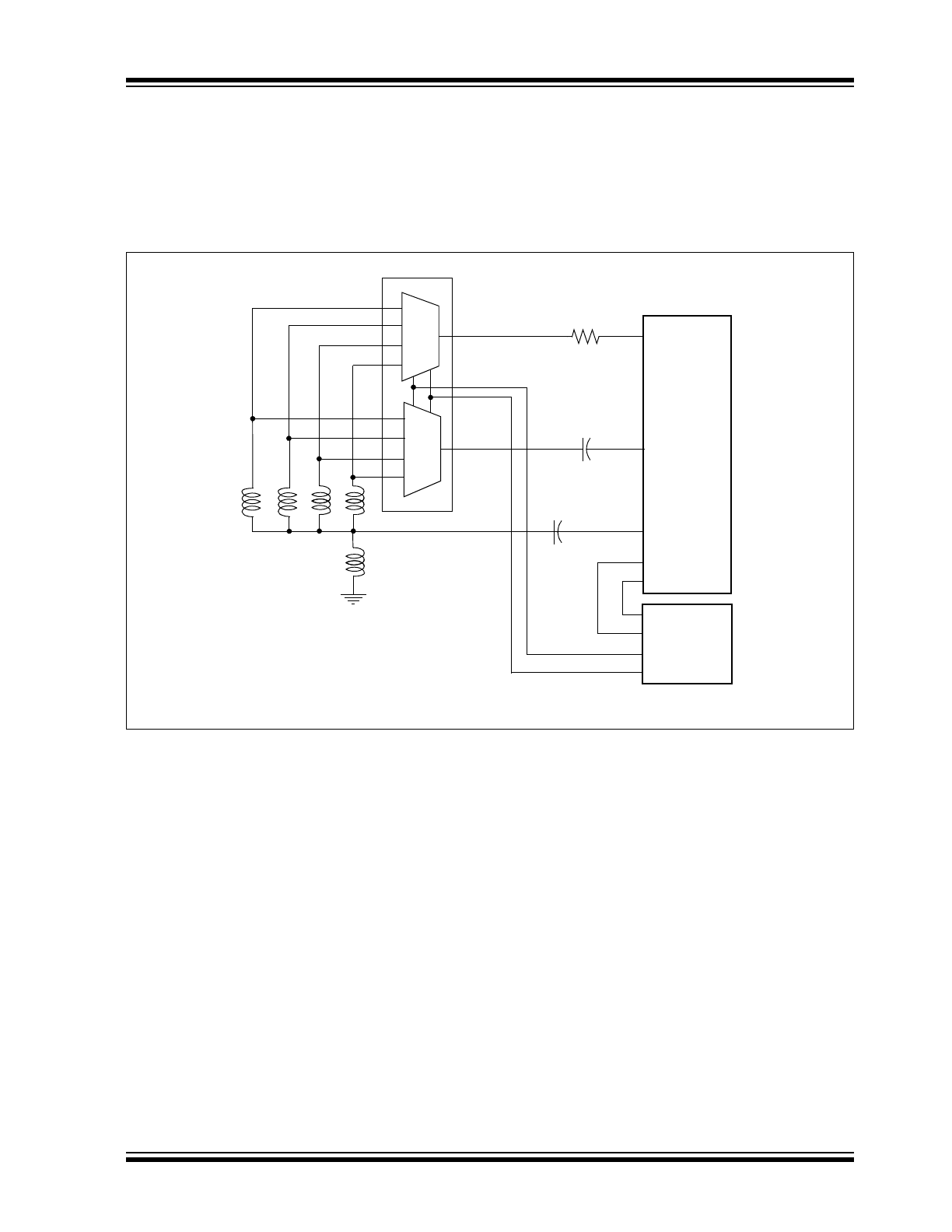
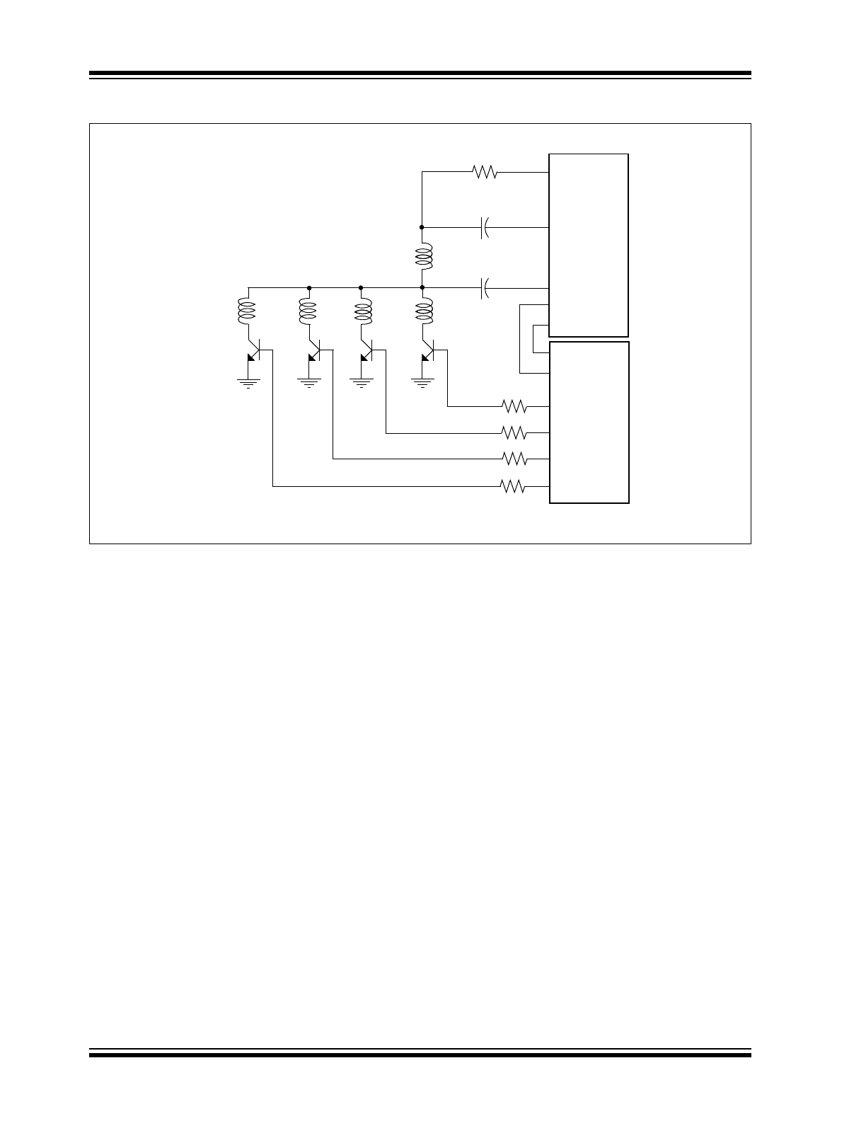
For an inductive touch system, two methods are used
for switching the driver and measurement circuitry
between the different sensor coils: analog multiplexers
and GPIO grounding (see
Figure 3-1
and
Figure 3-2
).
The MCP2036 is designed to work with both
configurations:
FIGURE 3-1:
Using Analog-Multiplexer for Key Selection (Example)
MCP2036
LREF
LBTN
LREF
DRVOUT
10
Ω
10nF
REFSEL
10nF
I/O
I/O
I/O
0
1
2
3
0
1
3
2
CD4052
Key Coils
PIC
®
Microcontroller
ISOL
I/O
MCP2036
DS22186C-page 8
© 2009 Microchip Technology Inc.
FIGURE 3-2:
Using NPN transistors for Key Selection (Example)
LREF
MCP2036
LBTN
LREF
DRVOUT
REFSEL
I/O
I/O
10
Ω
10nF
I/O
I/O
10nF
4K7
4K7
PIC
®
Microcontroller
I/O
4K7
4K7
Key Coils
ISOL
I/O
© 2009 Microchip Technology Inc.
DS22186C-page 9
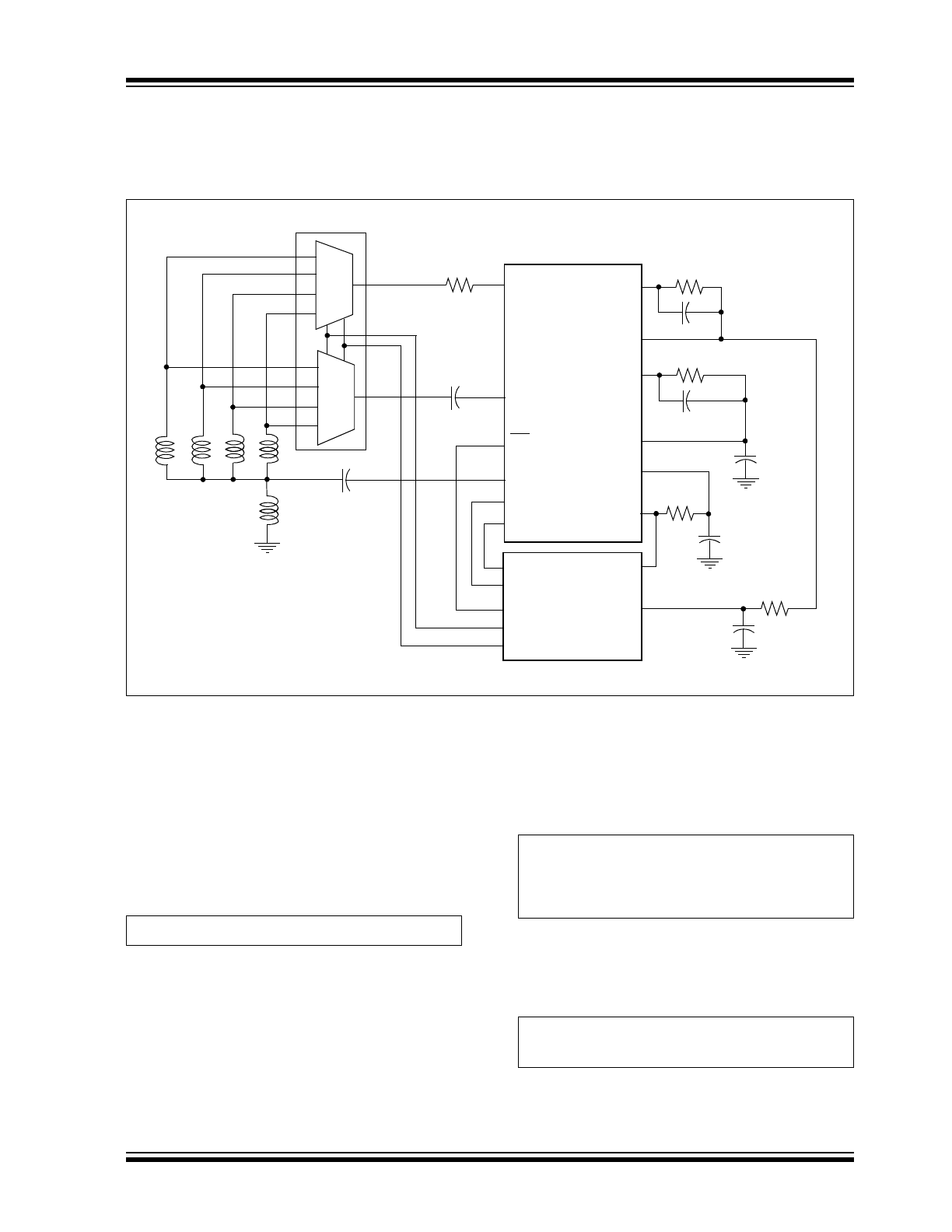
MCP2036
3.1
Application example
Figure 3-3
shows an example for a 4-key Inductive
Touch keyboard with key controlled by the IO pins of
the PIC
®
MCU.
FIGURE 3-3:
MCP2036 Typical Application
The PIC
®
microcontroller is used to generate a square
wave signal and to do all the necessary operations for
proper detection of the key press event.
Then, R
IN
-C
IN
filter converts the square wave output of
the PWM into a quasi-triangular waveform.
To calculate the amplitude of the triangular signal, the
standard charging time equation for an RC network will
be used, as shown in
Equation 3-1
:
EQUATION 3-1:
For the first half of the square wave, the capacitor C
IN
is charged through R
IN
, for the second half, it is
discharged through R
IN
, and assuming that clock
signal has a 50% duty cycle factor, we can consider:
EQUATION 3-2:
When the PWM signal switches from low-to-high or
from high-to-low, the step voltage applied to the
capacitor C
IN
will be:
EQUATION 3-3:
MCP2036
LREF
LBTN
LREF
DRVOUT
10
Ω
10nF
REFSEL
10nF
I/O
I/O
I/O
0
1
2
3
0
1
3
2
CD4052
Key Coils
PIC
®
Microcontroller
CS
I/O
V
DET-
V
DETOUT
V
DET+
V
REF
CLK
DRVIN
PWM
ADC
C
FILTER
C
FILTER
R
GAIN
R
GAIN
C
RGND
R
IN
C
IN
R
ADC
C
ADC
ISOL
I/O
V t
( ) V
step
1
t RC
⁄
–
(
)
exp
–
[
]
•
=
V
start
V
DD
2
⁄ -ΔV
=
V
stop
V
DD
2
⁄ +ΔV
=
V
step
V
DD
2
⁄
ΔV
+
(
)
=

MCP2036
DS22186C-page 10
© 2009 Microchip Technology Inc.
Substituting in the equation for an RC network:
EQUATION 3-4:
The peak-to-peak amplitude of the resulting triangular
waveform, at the coil driver input, is shown in
Equation 3-5
:
EQUATION 3-5:
From the previous equation, the designer should
choose values for V
PKPK
and R
IN
. Using the equation
above, the value of C
IN
will be:
EQUATION 3-6:
The amplitude of the pulsed current applied to key
inductors will be:
EQUATION 3-7:
This current produces a pulsed voltage to key inductors
ends. The amplitude of this voltage will be:
EQUATION 3-8:
The total voltage across both the reference and sensor
coils would be double (two series inductors). For a
specific power supply voltage, half of this power supply,
relative to the voltage reference, is available for output
amplifier/detector. Assuming a 30% margin, the
desired gain for the detector should be about:
EQUATION 3-9:
The gain of the amplifier is user-settable, using an
external resistor, R
GAIN.
The value of that resistor will
be determined using the following equation:
EQUATION 3-10:
With a 10-bit ADC, using oversampling and averaging
techniques, the effective resolution is close to 11 bits.
As shown in AN1239, “Inductive Touch Sensor
Design
”, the typical shift in sensor impedance is typi-
cally 3-4%, so the actual number of counts per press is
typically between 20 and 40 counts. In this way, the
microcontroller firmware could easily detect press
event.
Note:
V
PKPK
should not exceed specified value
(600mV) for best performance.
Note:
Assuming a power supply of 5V and
V
PKPK
=500mV, for R
IN
=3.9K
Ω, C
IN
should
have about 320pF. A 330pF capacitor will
be used.
ΔV
V
DD
2
-----------
1
t
–
R
IN
C
IN
------------------
⎝
⎠
⎛
⎞
exp
–
1
t
–
R
IN
C
IN
------------------
⎝
⎠
⎛
⎞
exp
+
-------------------------------------------
•
=
2
ΔV
V
DD
2
⁄
ΔV
+
(
)
1
t RC
⁄
–
(
)
exp
–
[
]
•
=
V
PK PK
2
ΔV
=
V
PKPK
V
DD
1
t
–
R
IN
C
IN
------------------
⎝
⎠
⎛
⎞
exp
–
1
t
–
R
IN
C
IN
------------------
⎝
⎠
⎛
⎞
exp
+
-------------------------------------------
•
=
C
IN
t
R
IN
ln
V
DD
V
PKPK
–
V
DD
V
PKPK
+
----------------------------------------
⎝
⎠
⎜
⎟
⎛
⎞
•
-------------------------------------------------------------------
1
2
F
R
IN
V
DD
V
PKPK
–
V
DD
V
PKPK
+
----------------------------------------
⎝
⎠
⎜
⎟
⎛
⎞
ln
•
•
•
-------------------------------------------------------------------------------------
=
=
ΔI V
PK PK
G
DRV
•
=
G
DRV
- Gain of Coil Driver
Note:
For a PWM frequency of 2 MHz and
inductor value of 2.7µH, the amplitude of
pulsed voltage will be:
Note:
For a power supply of 5V and
ΔU = 10mV,
the resulted gain is 81. To obtain this gain,
R
GAIN
= 820kOhm should be used.
ΔU L ΔI
Δt
------
•
L
V
PK PK
G
DRV
•
•
2F
•
=
=
F
- PWM Frequency
L
- Inductance of Key Inductor
ΔU 10.8mV
=
Gain
70%
V
DD
2
-----------
⎝
⎠
⎛
⎞
•
2
ΔU
•
---------------------------------
=
Gain
R
GAIN
/10kOhm
∼