
2005-2013 Microchip Technology Inc.
DS21981B-page 1
MCP2030
Device Features:
• Three input pins for analog input signals
• High input detection sensitivity (3 mV
PP
, typical)
• High modulation depth sensitivity (as low as 8%)
• Three output selections:
- Demodulated data
- Carrier clock
- RSSI
• Input carrier frequency: 125 kHz, typical
• Input data rate: 10 Kbps, maximum
• 8 internal Configuration registers
• Bidirectional transponder communication
(LF talk back)
• Programmable antenna tuning capacitance
(up to 63 pF, 1 pF/step)
• Programmable output enable filter
• Low standby current: 4
A (with 3 channels
enabled), typical
• Low operating current: 13
A (with 3 channels
enabled), typical
• Serial Peripheral Interface (SPI™) with external
devices
• Supports Battery Back-Up mode and batteryless
operation with external circuits
• Industrial and Extended Temperature Range:
-40°C to +85°C (industrial)
Typical Applications:
• Automotive industry applications:
- Passive Keyless Entry (PKE) transponder
- Remote door locks and gate openers
- Engine immobilizer
- LF initiator sensor for tire pressure monitoring
systems
• Security Industry applications:
- Long range access control transponder
- Parking lot entry transponder
- Hands-free apartment door access
- Asset control and management
Description:
The MCP2030 is a stand-alone Analog Front-End
(AFE) device for Low-Frequency (LF) sensing and bidi-
rectional communication applications. The device has
eight internal Configuration registers which are
readable and programmable, except the read-only
STATUS register, by an external device.
The device has three low-frequency input channels.
Each input channel can be individually enabled or dis-
abled. The device can detect an input signal with ampli-
tude as low as ~1 mV
PP
and can demodulate an
amplitude-modulated input signal with as low as 8%
modulation depth. The device can also transmit data by
clamping and unclamping the input LC antenna
voltage.
The device can output demodulated data, carrier clock
or RSSI current depending on the register setting. The
demodulated data and carrier clock outputs are avail-
able on the LFDATA pin, while the RSSI output is avail-
able on the RSSI pin. The RSSI current output is
linearly proportional to the input signal strength.
The device has programmable internal tuning capaci-
tors for each input channel. The user can program
these capacitors up to 63 pF, 1 pF per step. These
internal tuning capacitors can be used effectively for
fine-tuning of the external LC resonant circuit.
The device is optimized for very low current consump-
tion and has various battery-saving low-power modes
(Sleep, Standby, Active). The device can also be oper-
ated in Battery Back-up and Batteryless modes using a
few external components.
This device is available in 14-pin PDIP, SOIC, and
TSSOP packages. This device is also used as the AFE
in the PIC16F639.
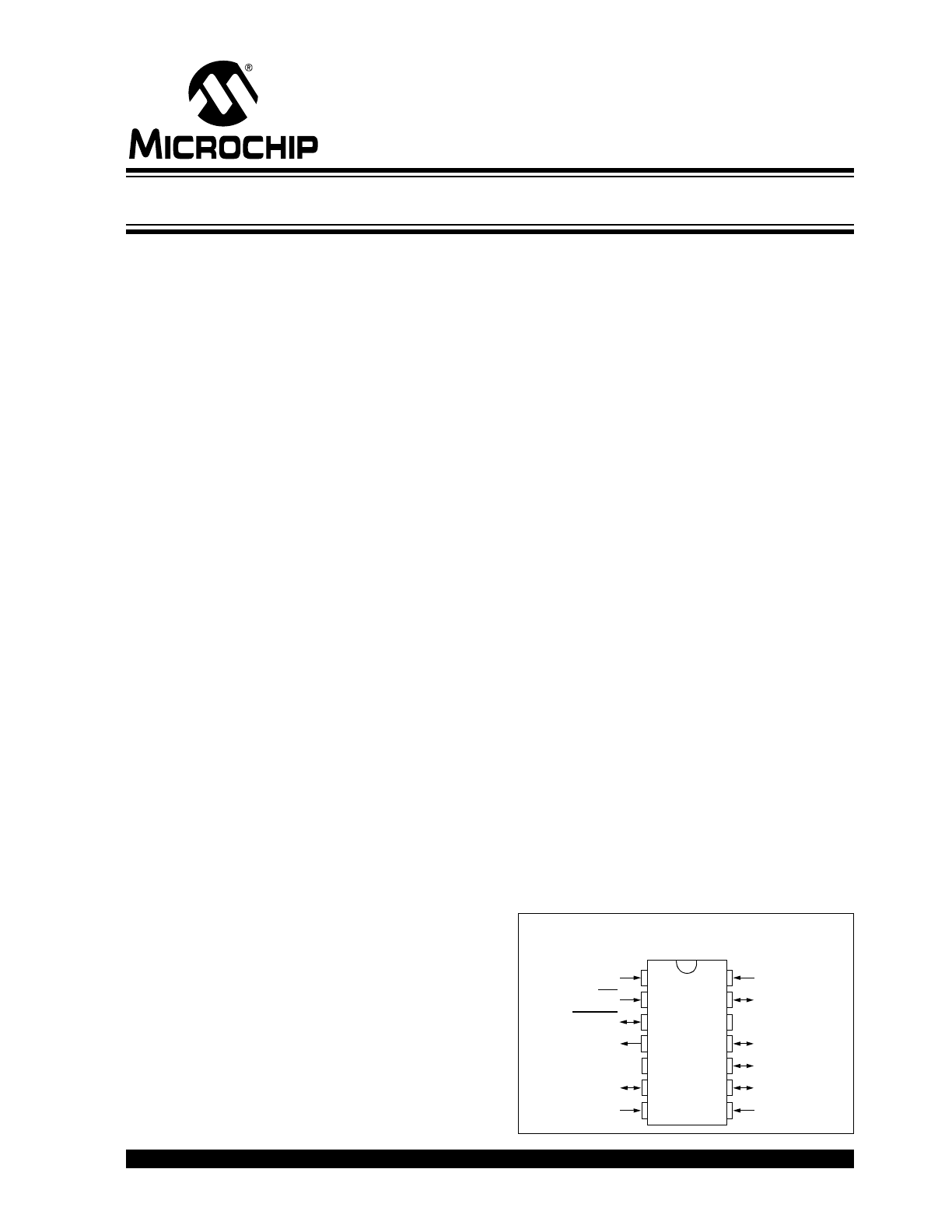
Package Types:
1
2
3
4
5
6
7
14
13
12
9
11
10
8
NC
LCCOM
LCX
V
SS
LFDATA/
V
DD
LCZ
LCY
V
SS
CS
SCLK/ALERT
RSSI
NC
V
DD
CCLK/SDIO
MCP2030
PDIP, SOIC, TSSOP
Three-Channel Analog Front-End Device

MCP2030
DS21981B-page 2
2005-2013 Microchip Technology Inc.
NOTES:
2005-2013 Microchip Technology Inc.
DS21981B-page 3
MCP2030
1.0
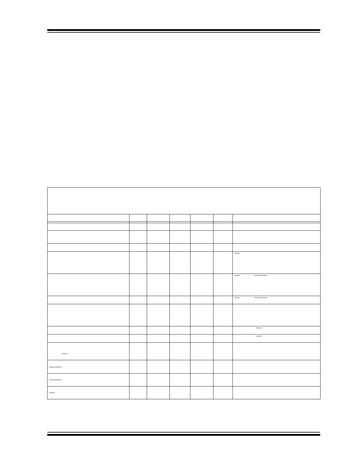
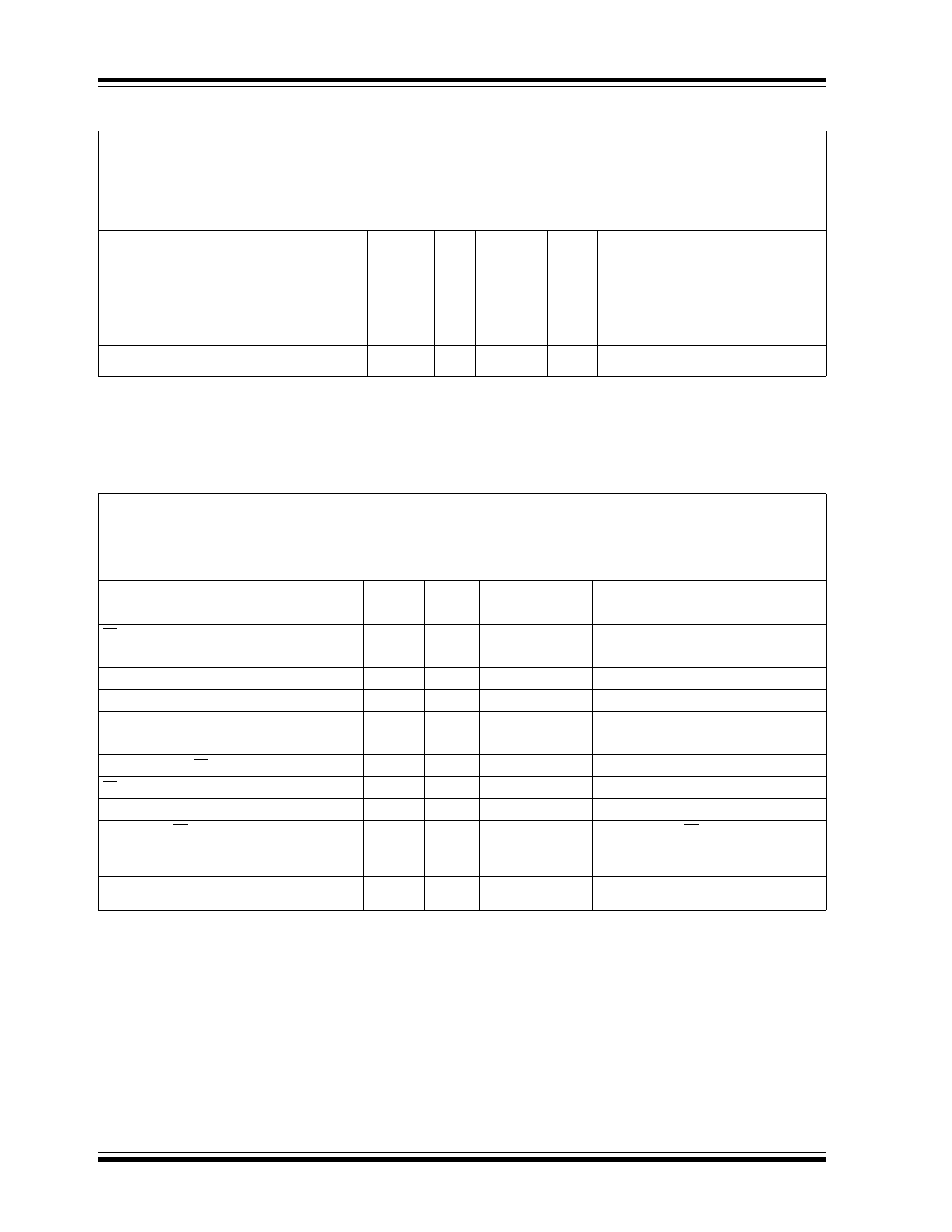
ELECTRICAL SPECIFICATIONS
Absolute Maximum Ratings
(†)
Ambient temperature under bias...................-40°C to +125°C
Storage temperature .................................... -65°C to +150°C
Voltage on V
DD
with respect to V
SS
............... -0.3V to +6.5V
Voltage on all other pins with
respect to V
SS
...................................... -0.3V to (V
DD
+ 0.3V)
Maximum current out of V
SS
pin .................................300 mA
Maximum current into V
DD
pin ....................................250 mA
Maximum LC Input Voltage
(LCX, LCY, LCZ) loaded, with device........................ 10.0 V
PP
Maximum LC Input Voltage
(LCX, LCY, LCZ) unloaded, without device............. 700.0 V
PP
Maximum Input Current (rms) into device
per LC Channel .............................................................10 mA
Human Body ESD rating ....................................2000 (min.) V
Machine Model ESD rating ..................................200 (min.) V
† Notice: Stresses above those listed under “Maximum
Ratings” may cause permanent damage to the device. This is
a stress rating only and functional operation of the device at
those or any other conditions above those indicated in the
operation listings of this specification is not implied. Exposure
to maximum rating conditions for extended periods may affect
device reliability.
DC Characteristics
Electrical Specifications: Standard Operating Conditions (unless otherwise stated)
Operating temperature
-40
C T
A
+85C
LC Signal Input
Sinusoidal 300 mV
PP
Carrier Frequency
125 kHz
LCCOM connected to V
SS
Parameters
Sym.
Min.
Typ†
Max.
Units
Conditions
Supply Voltage
V
DD
2.0
3.0
3.6
V
V
DD
Start Voltage to ensure internal
Power-on Reset signal
V
POR
—
—
1.8
V
Modulation Transistor-on Resistance
R
M
—
50
100
V
DD
= 3.0V
Active Current (detecting signal)
1 LC Input Channel Receiving Signal
3 LC Input Channel Receiving Signals
I
ACT
—
—
10
13
—
18
A
A
CS = V
DD
Input = Continuous Wave (CW);
Amplitude = 300 mV
PP
.
All channels enabled.
Standby Current (wait to detect signal)
1 LC Input Channel Enabled
2 LC Input Channels Enabled
3 LC Input Channels Enabled
I
STDBY
—
—
—
2
3
4
5
6
7
A
A
A
CS = V
DD
; ALERT = V
DD
Sleep Current
I
SLEEP
—
0.2
1
A
CS = V
DD
; ALERT = V
DD
Analog Input Leakage Current
LCX, LCY, LCZ
LCCOM
I
AIL
—
—
—
—
1
1
A
A
V
DD
= 3.6V, V
SS
V
IN
1V with respect to
ground. Internal tuning capacitors are switched
off, tested in Sleep mode.
Digital Input Low Voltage
V
IL
V
SS
—
0.3 V
DD
V
SCLK, SDI, CS
Digital Input High Voltage
V
IH
0.8 V
DD
—
V
DD
V
SCLK, SDI, CS
Digital Input Leakage Current (Note 1)
SDI
SCLK, CS
I
IL
—
—
—
—
1
1
A
A
V
DD
= 3.6V
V
SS
V
PIN
V
DD
V
PIN
V
DD
Digital Output Low Voltage
ALERT, LFDATA/SDIO
V
OL
—
—
V
SS
+
0.4
V
Analog Front-End section
I
OL
= 1.0 mA, V
DD
= 2.0V
Digital Output High Voltage
ALERT, LFDATA/SDIO
V
OH
V
DD
- 0.5
—
—
V
I
OH
= -400
A, V
DD
= 2.0V
Digital Input Pull-Up Resistor
CS, SCLK
R
PU
50
200
350
k
V
DD
= 3.6V
*
These parameters are characterized but not tested.
†
Data in “Typ” column is at 3.0V, +25
C unless otherwise stated. These parameters are for design guidance only and are not tested.
Note
1:
Negative current is defined as current sourced by the pin.
MCP2030
DS21981B-page 4
2005-2013 Microchip Technology Inc.
AC Characteristics
Electrical Specifications: Standard Operating Conditions (unless otherwise stated)
Supply Voltage
2.0V
V
DD
3.6V
Operating temperature
-40°C
T
A
+85°C
LCCOM connected to V
SS
LC Signal Input
Sinusoidal 300 mV
PP
Carrier Frequency
125 kHz
LCCOM connected to V
SS
Parameters
Sym.
Min.
Typ†
Max.
Units
Conditions
Input Sensitivity
V
SENSE
1
3.0
6
mV
PP
V
DD
= 3.0V
Output enable filter disabled
AGCSIG = 0; MODMIN = 00
(33% modulation depth setting)
Input = Continuous Wave (CW)
Output = Logic level transition from
low-to-high at sensitivity level for CW input.
Coil de-Q’ing Voltage -
RF Limiter (R
FLM
) must be active
V
DE_Q
3
—
5
V
V
DD
= 3.0V, Force I
IN
= 5
A (worst case)
RF Limiter Turn-on Resistance
(LCX, LCY, LCZ)
R
FLM
—
300
700
V
DD
= 2.0V, V
IN
= 8 V
DC
Sensitivity Reduction
S
ADJ
—
—
0
-30
—
—
dB
dB
V
DD
= 3.0V
No sensitivity reduction selected
Max. reduction selected
Monotonic increment in attenuation value
from setting = 0000 to 1111 by design
Minimum Modulation Depth
60% setting
33% setting
14% setting
8%
V
IN_MOD
—
—
—
60
33
14
8
84
49
26
%
%
%
%
V
DD
= 3.0V
See Section 5.21 “Minimum Modulation
Depth Requirement for Input Signal”.
See Modulation Depth Definition in
Figure 5-5.
Carrier frequency
F
CARRIER
—
125
—
kHz
Input modulation frequency
F
MOD
—
—
10
kHz
Input data rate with NRZ data format.
V
DD
= 3.0V
Minimum modulation depth setting = 33%
Input conditions:
Amplitude = 300 mV
PP
Modulation depth = 100%
LCX Tuning Capacitor
C
TUNX
—
44
0
59
—
82
pF
pF
V
DD
= 3.0V,
Config. Reg. 1, bits <6:1> Setting = 000000
63 pF ±30%
Config. Reg. 1, bits <6:1> Setting = 111111
63 steps, approx. 1 pF/step
Monotonic increment in capacitor value from
setting = 000000 to 111111 by design
LCY Tuning Capacitor
C
TUNY
—
44
0
59
—
82
pF
pF
V
DD
= 3.0V,
Config. Reg. 2, bits <6:1> Setting = 000000
63 pF ±30%
Config. Reg. 2, bits <6:1> Setting = 111111
63 steps, approx. 1 pF/step
Monotonic increment in capacitor value from
setting = 000000 to 111111 by design
LCZ Tuning Capacitor
C
TUNZ
—
44
0
59
—
82
pF
pF
V
DD
= 3.0V,
Config. Reg. 3, bits<6:1> Setting = 000000
63 pF ±30%
Config. Reg. 3, bits<6:1> Setting = 111111
63 steps, approx. 1 pF/step
Monotonic increment in capacitor value from
setting = 000000 to 111111 by design
Q of Internal Tuning Capacitors
Q_C
50 *
—
—
Demodulator Charge Time
(delay time of demodulated output to rise)
T
DR
—
50
—
s
V
DD
= 3.0V
Minimum modulation depth setting = 33%
Input conditions:
Amplitude = 300 mV
PP
Modulation depth = 100%
*
Parameter is characterized but not tested.
†
Data in “Typ” column is at 3.0V, 25°C unless otherwise stated. These parameters are for design guidance only and are not tested.
Note
1:
Required output enable filter high time must account for input path analog delays (= T
OEH
- T
DR
+ T
DF
).
2:
Required output enable filter low time must account for input path analog delays (= T
OEL
+ T
DR
- T
DF
).
2005-2013 Microchip Technology Inc.
DS21981B-page 5
MCP2030
Demodulator Discharge Time (delay time
of demodulated output to fall)
T
DF
—
50
—
s
V
DD
= 3.0V
MOD depth setting = 33%
Input conditions:
Amplitude = 300 mV
PP
Modulation depth = 100%
Rise time of LFDATA
TR
LFDATA
—
0.5
—
s
V
DD
3.0V. Time is measured from 10% to
90% of amplitude
Fall time of LFDATA
TF
LFDATA
—
0.5
—
s
V
DD
3.0V
Time is measured from 10% to 90% of
amplitude
AGC stabilization time
(T
AGC +
T
PAGC
)
T
STAB
4
—
—
ms
AGC initialization time
T
AGC
—
3.5
—
ms
High time after AGC initialization time
T
PAGC
—
62.5
—
s
Gap time after AGC stabilization time
T
GAP
200
—
—
s
Time element of pulse
T
E
100
—
—
s
Minimum pulse width
Time from exiting Sleep or POR to being
ready to receive signal
T
RDY
—
—
50*
ms
Minimum time AGC level must be held
after receiving AGC Preserve command
T
PRES
5*
—
—
ms
AGC level must not change more than 10%
during T
PRES
.
Internal RC oscillator frequency
F
OSC
27
32
35.5
kHz
Internal clock trimmed at 32 kHz during test
Inactivity timer time-out
T
INACT
13.5
16
17.75
ms
512 cycles of RC oscillator @ F
OSC
Alarm timer time-out
T
ALARM
27
32
35.5
ms
1024 cycles of RC oscillator @ F
OSC
LC Pin Input Resistance for
LCX, LCY, LCZ pins
R
IN
—
800*
—
k
LCCOM grounded, V
DD
= 3V,
F
CARRIER
= 125 kHz.
LC Pin Input Parasitic Capacitance for
LCX, LCY, LCZ pins
C
IN
—
24*
—
pF
LCCOM grounded, V
DD
= 3V,
F
CARRIER
= 125 kHz.
Minimum output enable filter high time
OEH (Bits Config0<8:7>)
01
= 1 ms
10
= 2 ms
11
= 4 ms
00
= Filter Disabled
T
OEH
32 (~1 ms)
64 (~2 ms)
128 (~4 ms)
—
—
—
—
—
—
—
—
—
clock
count
RC oscillator = F
OSC
(see F
OSC
specification
for variations).
Viewed from the pin input:
(Note 1)
Minimum output enable filter low time
OEL (Bits Config0<6:5>)
00
= 1 ms
01
= 1 ms
10
= 2 ms
11
= 4 ms
T
OEL
32 (~1 ms)
32 (~1 ms)
64 (~2 ms)
128 (~4 ms)
—
—
—
—
—
—
—
—
clock
count
RC oscillator = F
OSC
Viewed from the pin input:
(Note 2)
Maximum output enable filter period
OEH
OEL
T
OEH
T
OEL
01
00
= 1 ms
1 ms (Filter 1)
01
01
= 1 ms
1 ms (Filter 1)
01
10
= 1 ms
2 ms (Filter 2)
01
11
= 1 ms
4 ms (Filter 3)
T
OET
—
—
—
—
—
—
—
—
96 (~3 ms)
96 (~3 ms)
128 (~4 ms)
192 (~6 ms)
clock
count
RC oscillator = F
OSC
10
00
= 2 ms
1 ms (Filter 4)
10
01
= 2 ms
1 ms (Filter 4)
10
10
= 2 ms
2 ms (Filter 5)
10
11
= 2 ms
4 ms (Filter 6)
—
—
—
—
—
—
—
—
128 (~4 ms)
128 (~4 ms)
160 (~5 ms)
250 (~8 ms)
11
00
= 4 ms
1 ms (Filter 7)
11
01
= 4 ms
1 ms (Filter 7)
11
10
= 4 ms
2 ms (Filter 8)
11
11
= 4 ms
4 ms (Filter 9)
—
—
—
—
—
—
—
—
192 (~6 ms)
192 (~6 ms)
256 (~8 ms)
320 (~10 ms)
00
XX
= Filter Disabled
—
—
—
LFDATA output appears as long as input
signal level is greater than V
SENSE
.
AC Characteristics (Continued)
Electrical Specifications: Standard Operating Conditions (unless otherwise stated)
Supply Voltage
2.0V
V
DD
3.6V
Operating temperature
-40°C
T
A
+85°C
LCCOM connected to V
SS
LC Signal Input
Sinusoidal 300 mV
PP
Carrier Frequency
125 kHz
LCCOM connected to V
SS
Parameters
Sym.
Min.
Typ†
Max.
Units
Conditions
*
Parameter is characterized but not tested.
†
Data in “Typ” column is at 3.0V, 25°C unless otherwise stated. These parameters are for design guidance only and are not tested.
Note
1:
Required output enable filter high time must account for input path analog delays (= T
OEH
- T
DR
+ T
DF
).
2:
Required output enable filter low time must account for input path analog delays (= T
OEL
+ T
DR
- T
DF
).
MCP2030
DS21981B-page 6
2005-2013 Microchip Technology Inc.
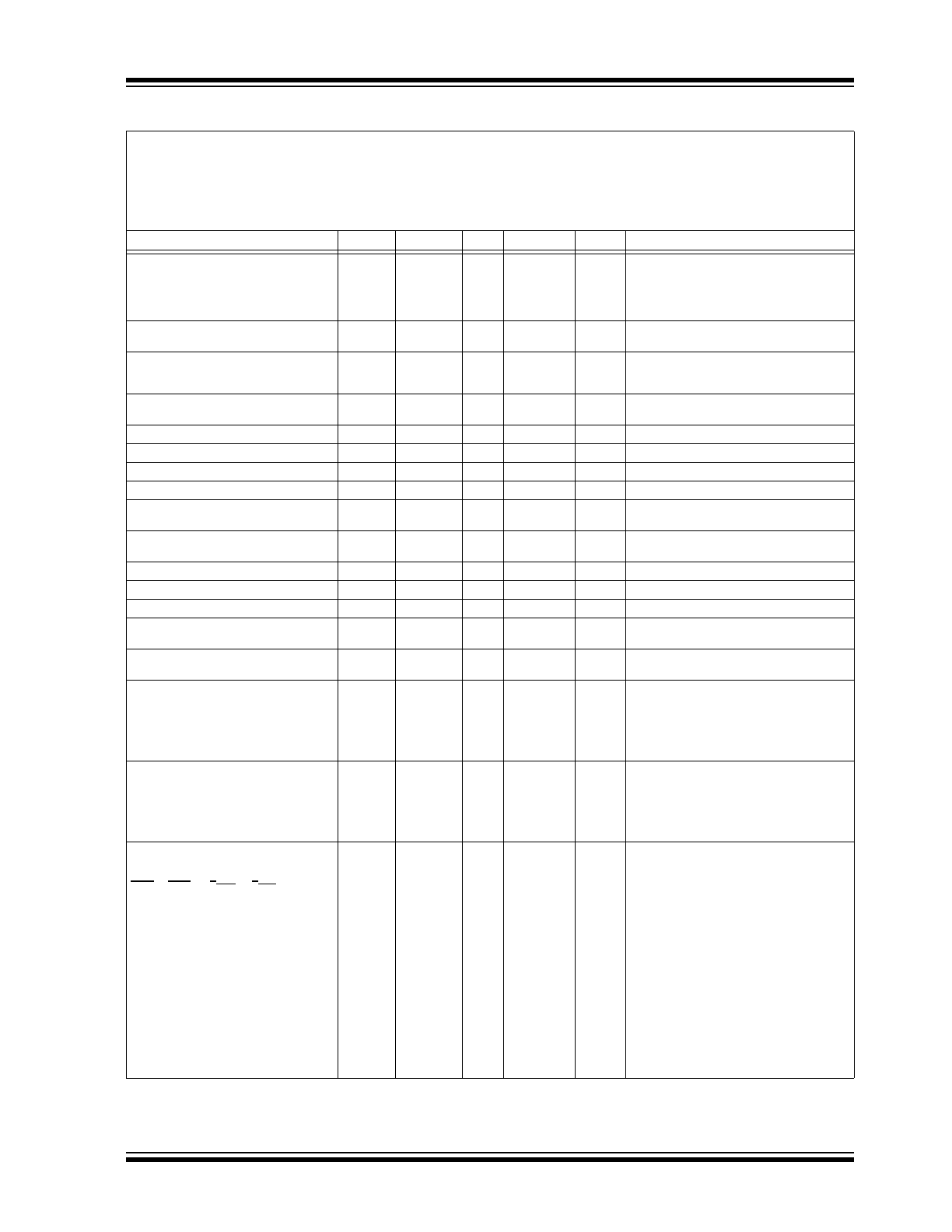
RSSI current output
I
RSSI
—
6
—
0.65
12
100
2
20.3
—
A
A
A
V
IN
= 37 mV
PP
V
IN
= 370 mV
PP
V
DD
= 3.0V, V
IN
= 0 to 4 V
PP
Linearly increases with input signal ampli-
tude.
Tested at V
IN
= 37 mV
PP
, 100 mV
PP
, and
370 mV
PP
at +25ºC.
RSSI current linearity
ILR
RSSI
-15
—
15
%
Tested at room temperature only (see
Equation 5-1 and Figure 5-7 for test method).
AC Characteristics (Continued)
Electrical Specifications: Standard Operating Conditions (unless otherwise stated)
Supply Voltage
2.0V
V
DD
3.6V
Operating temperature
-40°C
T
A
+85°C
LCCOM connected to V
SS
LC Signal Input
Sinusoidal 300 mV
PP
Carrier Frequency
125 kHz
LCCOM connected to V
SS
Parameters
Sym.
Min.
Typ†
Max.
Units
Conditions
*
Parameter is characterized but not tested.
†
Data in “Typ” column is at 3.0V, 25°C unless otherwise stated. These parameters are for design guidance only and are not tested.
Note
1:
Required output enable filter high time must account for input path analog delays (= T
OEH
- T
DR
+ T
DF
).
2:
Required output enable filter low time must account for input path analog delays (= T
OEL
+ T
DR
- T
DF
).
SPI Timing
Electrical Specifications: Standard Operating Conditions (unless otherwise stated)
Supply Voltage
2.0V
V
DD
3.6V
Operating temperature
-40°C
T
A
+85°C
LC Signal Input
Sinusoidal 300 mV
PP
Carrier Frequency
125 kHz
LCCOM connected to V
SS
Parameters
Sym.
Min.
Typ†
Max.
Units
Conditions
SCLK Frequency
F
SCLK
—
—
3
MHz
CS fall to first SCLK edge setup time
T
CSSC
100
—
—
ns
SDI setup time
T
SU
30
—
—
ns
SDI hold time
T
HD
50
—
—
ns
SCLK high time
T
HI
150
—
—
ns
SCLK low time
T
LO
150
—
—
ns
SDO setup time
T
DO
—
—
150
ns
SCLK last edge to CS rise setup time
T
SCCS
100
—
—
ns
CS high time
T
CSH
500
—
—
ns
CS rise to SCLK edge setup time
T
CS1
50
—
—
ns
SCLK edge to CS fall setup time
T
CS0
50
—
—
ns
SCLK edge when CS is high
Rise time of SPI data
(SPI Read command)
TR
SPI
—
10
—
ns
V
DD
3.0V. Time is measured from 10% to
90% of amplitude
Fall time of SPI data
(SPI Read command)
TF
SPI
—
10
—
ns
V
DD
3.0V. Time is measured from 90% to
10% of amplitude
†
Data in “Typ” column is at 3.0V, 25°C unless otherwise stated. These parameters are for design guidance only and are not tested.
2005-2013 Microchip Technology Inc.
DS21981B-page 7
MCP2030
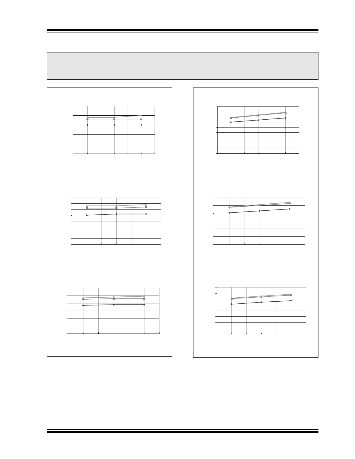
2.0
TYPICAL PERFORMANCE CURVES
FIGURE 2-1:
Typical Standby Current.
FIGURE 2-2:
Typical Active Current.
Note:
The graphs and tables provided following this note are a statistical summary based on a limited number of
samples and are provided for informational purposes only. The performance characteristics listed herein
are not tested or guaranteed. In some graphs or tables, the data presented may be outside the specified
operating range (e.g., outside specified power supply range) and therefore outside the warranted range.
Standby Current (3 Channels Enabled)
0
1
2
3
4
5
6
2 V
3 V
3.6 V
V
DD
(V)
Cu
rren
t Draw
(
A)
Standby Current (2 Channels Enabled)
0
0.5
1
1.5
2
2.5
3
3.5
4
2 V
3 V
3.6 V
V
DD
(V)
Cu
rren
t Draw
(
A)
Standby Current (1 Channel Enabled)
0
0.5
1
1.5
2
2.5
2 V
3 V
3.6 V
V
DD
(V)
Cu
rren
t Draw
(
A)
+85
C
+25
C
-40
C
+85
C
+25
C
-40
C
+85
C
+25
C
-40
C
Active Current (3 Channels Enabled)
0
2
4
6
8
10
12
14
16
2 V
3 V
3.6 V
V
DD
(V)
Cu
rren
t Draw
(
A)
Active Current (1 Channel Enabled)
0
1
2
3
4
5
6
7
8
9
2 V
3 V
3.6 V
V
DD
(V)
Cu
rren
t Draw
(
A)
Active Current (2 Channels Enabled)
0
2
4
6
8
10
12
2 V
3 V
3.6 V
V
DD
(V)
Cu
rren
t Draw
(
A)
+85
C
+25
C
-40
C
+85
C
+25
C
-40
C
+85
C
+25
C
-40
C
MCP2030
DS21981B-page 8
2005-2013 Microchip Technology Inc.
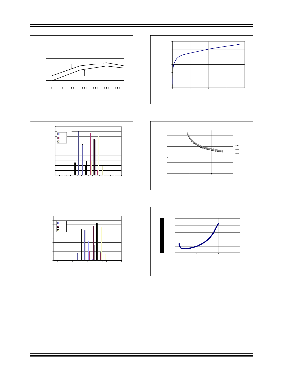
FIGURE 2-3:
Oscillator Frequency vs.
Temperature, V
DD
= 3.6V and 2.0V.
FIGURE 2-4:
Oscillator Frequency
Histograms vs. Temperature, V
DD
= 2V.
FIGURE 2-5:
Oscillator Frequency
Histograms vs. Temperature at V
DD
= 3V.
FIGURE 2-6:
De-Q’ed Voltage vs.
Unloaded Coil Voltage.
FIGURE 2-7:
Modulation Transistor-on
Resistance (+25°C).
FIGURE 2-8:
Channel Sensitivity vs.
Bandwidth.
29
30
31
32
33
34
35
-50
-25
0
25
50
75
100
125
Temperature (°C)
Osci
llator
Fr
equency (kH
z
.)
Osc. Freq. @ VDD = 3.6V
Osc. Freq. @ VDD = 2.0V
0.0%
5.0%
10.0%
15.0%
20.0%
25.0%
30.0%
35.0%
40.0%
45.0%
50.0%
27
28
29
30
31
32
33
34
35
Oscillator Frequency (kHz.)
Per
c
ent
a
ge of O
c
cur
e
nce
s
(
%
)
-40C
25C
85C
V
DD
= 2.0V
0.0%
5.0%
10.0%
15.0%
20.0%
25.0%
30.0%
35.0%
40.0%
45.0%
50.0%
27
28
29
30
31
32
33
34
35
Oscillator Frequency (kHz.)
Per
cent
a
ge of
O
ccur
e
nces
(%
)
-40C
25C
85C
V
DD
= 3.6V
0
2
4
6
8
10
12
0
200
400
600
800
Unloaded Coil Voltage (V
PP
)
D
e
-Q
'e
d (
L
oa
d
e
d
) C
o
il
Vo
lt
ag
e
(V
PP
)
0
10
20
30
40
50
60
70
80
0
2
4
6
V
DD
(V)
Oh
m
s
Ch. X
Ch. Y
Ch. Z
0
5
10
15
2 0
2 5
0
2 0 0
4 0 0
6 0 0
F re que nc y ( k H z)
2005-2013 Microchip Technology Inc.
DS21981B-page 9
MCP2030
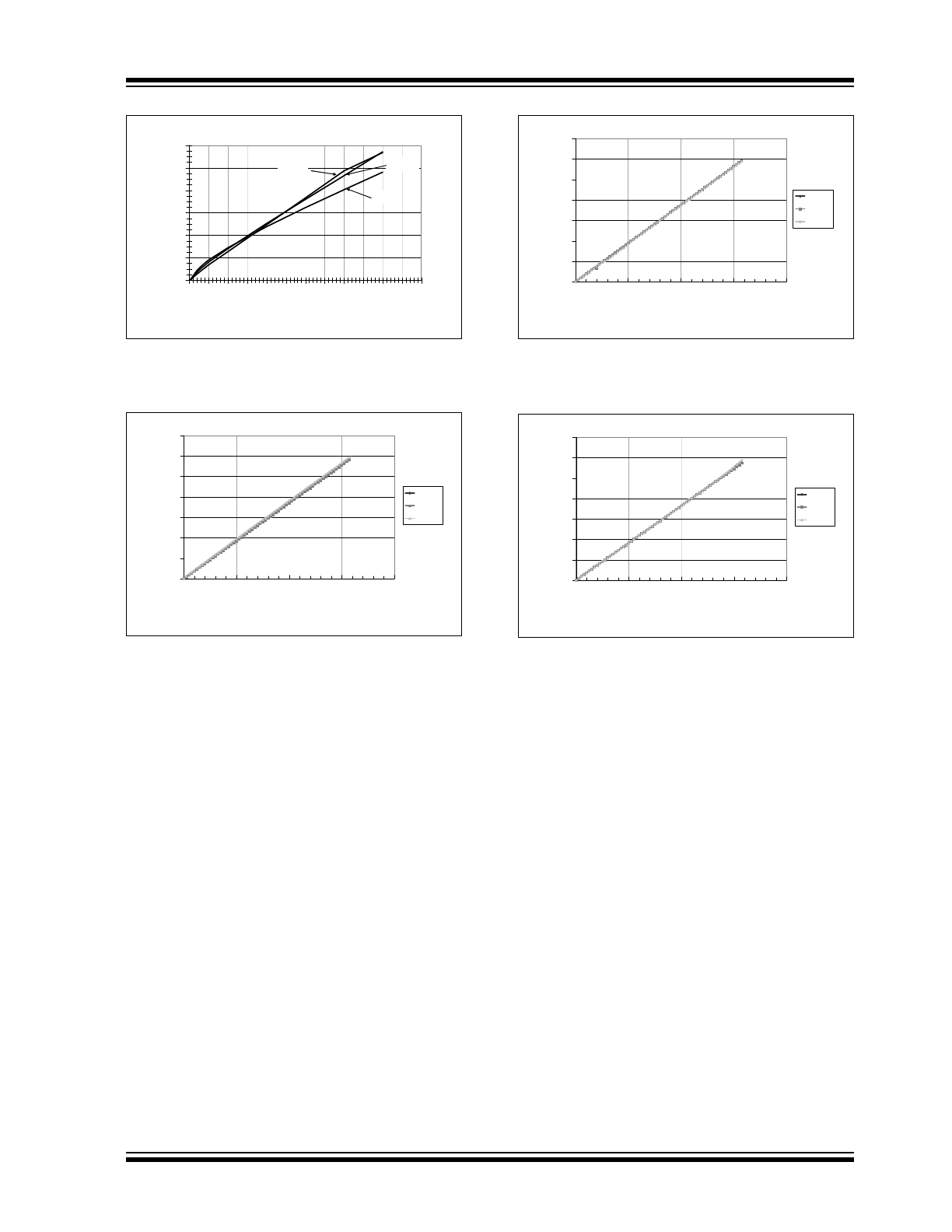
FIGURE 2-9:
Typical RSSI Output Current
vs. Input Signal Strength.
FIGURE 2-10:
Typical Tuned Capacitance
Value vs. Configuration Register Bit Setting
(V
DD
= 3V, Temperature = +25°C.
FIGURE 2-11:
Typical Tuned Capacitance
Value vs. Configuration Register Bit Setting
(V
DD
= 3V,Temperature = -40°C.
FIGURE 2-12:
Typical Tuned Capacitance
Value vs. Configuration Register Bit Setting
(V
DD
= 3V,Temperature = +85°C.
0
20
40
60
80
100
120
0
0.5
1
1.5
2
2.5
3
3.5
4
4.5
5
5.5
6
Input Voltage (V)
RS
SI (
µ
A)
-40°C
+85°C
+25°C
0
10
20
30
40
50
60
70
0
20
40
60
80
Bit Setting (Steps)
C
a
p
aci
ta
nce
(p
F)
Ch. X
Ch. Y
Ch. Z
0
10
20
30
40
50
60
70
0
20
40
60
80
Bit Setting (steps)
C
a
pa
cit
a
nc
e (
pF)
Ch. X
Ch. Y
Ch. Z
0
10
20
30
40
50
60
70
0
20
40
60
80
Bit Setting (Steps)
C
a
p
acit
a
nce (pF
)
Ch. X
Ch. Y
Ch. Z
MCP2030
DS21981B-page 10
2005-2013 Microchip Technology Inc.
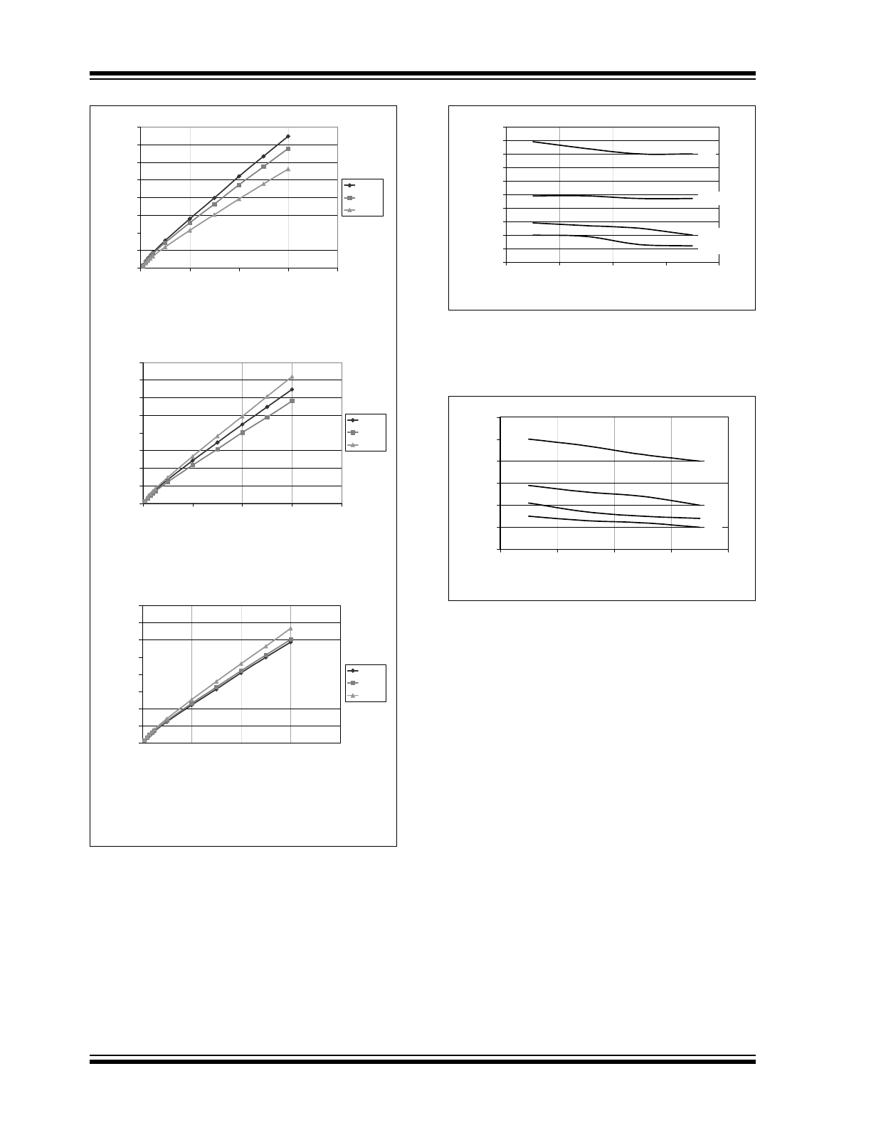
FIGURE 2-13:
Examples of RSSI Output
Current Variations Between Channel to Channel
and Device to Device at Room Temperature.
FIGURE 2-14:
Example of Typical T
DR
Changes over Temperature.
Input Signal Condition: Amplitude = 300 mV
PP
,
Modulation Depth = 100 %.
FIGURE 2-15:
Example of Typical T
DF
Changes over Temperature.
Input Signal Condition: Amplitude = 300 mV
PP
,
Modulation Depth = 100 %.
0
10
20
30
40
50
60
70
80
0
2
4
6
8
Input Voltage (V)
RSSI Cu
rr
e
n
t (
A)
Ch-X
Ch-Y
Ch-Z
0
10
20
30
40
50
60
70
80
0
2
4
6
8
Input Voltage (V)
RSSI Cu
rr
e
n
t (
A)
Ch-X
Ch-Y
Ch-Z
Device (a)
Device (b)
Device (c)
Note:
Equal amplitude is applied to each channel.
0
10
20
30
40
50
60
70
80
0
2
4
6
8
Input Voltage (V)
Curre
nt
(
A)
Ch-X
Ch-Y
Ch-Z
0
10
20
30
40
50
60
70
80
90
100
85C
25C
-20C
-40C
Temperature (°C)
T
DR
(µs
)
8%
14%
33%
60%
0
10
20
30
40
50
60
85C
25C
-20C
-40C
Temperature (°C)
T
DF
(µ
s
)
8%
14%
33%
60%