
2012-2014 Microchip Technology Inc.
DS20002298C-page 1
MCP2021A/2A
Features:
• The MCP2021A/2A are compliant with LIN Bus
Specifications Version 1.3, 2.1 and with SAE
J2602-2
• Support Baud Rates up to 20 kBaud
• 43V Load Dump Protected
• Maximum Continuous Input Voltage: 30V
• Wide LIN-Compliant Supply Voltage: 6.0 – 18.0V
• Extended Temperature Range: -40 to +125°C
• Interface to PIC
®
MCU EUSART and Standard
USARTs
• Wake-Up on LIN Bus Activity or Local Wake Input
• Local Interconnect Network (LIN) Bus Pin:
- Internal Pull-Up Termination Resistor and
Diode for Slave Node
- Protected Against V
BAT
Shorts
- Protected Against Loss of Ground
- High-Current Drive
• T
XD
and LIN Bus Dominant Time-Out Function
• Two Low-Power Modes:
- Transmitter Off: 90 µA (typical)
- Power Down: 4.5 µA (typical)
• Output Indicating Internal Reset State (POR or
Sleep Wake)
• MCP2021A/2A On-Chip Voltage Regulator:
- Output Voltage of 5.0V or 3.3V
at 70 mA Capability with Tolerances of ±3%
Over the Temperature Range
- Internal Short Circuit Current Limit
- External Components Limited to Filter
Capacitor and Load Capacitor
• Automatic Thermal Shutdown
• High Electromagnetic Immunity (EMI), Low
Electromagnetic Emission (EME)
• Robust ESD Performance: ±15 kV for L
BUS
and
V
BB
pin (IEC61000-4-2)
• Transient Protection for L
BUS
and V
BB
Pins in
Automotive Environment (ISO7637)
• Meets Stringent Automotive Design
Requirements, including “OEM Hardware
Requirements for LIN, CAN and FlexRay
Interfaces in Automotive Applications”, Version
1.2, March 2011
• Multiple Package Options, including Small
4x4 mm DFN Package
Description:
The MCP2021A/2A provide a bidirectional, half-duplex
communication physical interface to meet the LIN bus
specification Revision 2.1 and SAE J2602-2. The
devices incorporate a voltage regulator with 5V or 3.3V
at 70 mA regulated power supply output. The devices
have been designed to meet the stringent quiescent
current requirements of the automotive industry and
will survive +4
3
V load dump transients and double
battery jumps.
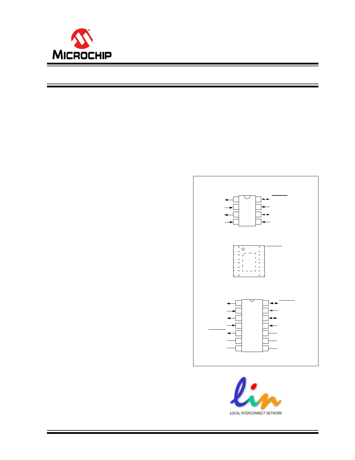
Package Types
MCP2021A
PDIP, SOIC
V
REG
CS/LWAKE
T
XD
1
2
3
4
8
7
6
5
R
XD
FAULT/T
XE
V
BB
L
BUS
V
SS
MCP2021A
4x4 DFN
V
REG
CS/LWAKE
T
XD
R
XD
FAULT/T
XE
V
BB
L
BUS
V
SS
1
2
3
4
8
7
6
5
EP
9
MCP2022A
PDIP, SOIC, TSSOP
V
REG
CS/LWAKE
T
XD
1
2
3
4
14
13
12
11
R
XD
FAULT/T
XE
V
BB
L
BUS
V
SS
RESET
5
10
NC
NC
6
9
NC
7
8
NC
NC
* Includes Exposed Thermal Pad (EP), see
Table 1-2
.
LIN Transceiver with Voltage Regulator
MCP2021A/2A
DS20002298C-page 2
2012-2014 Microchip Technology Inc.
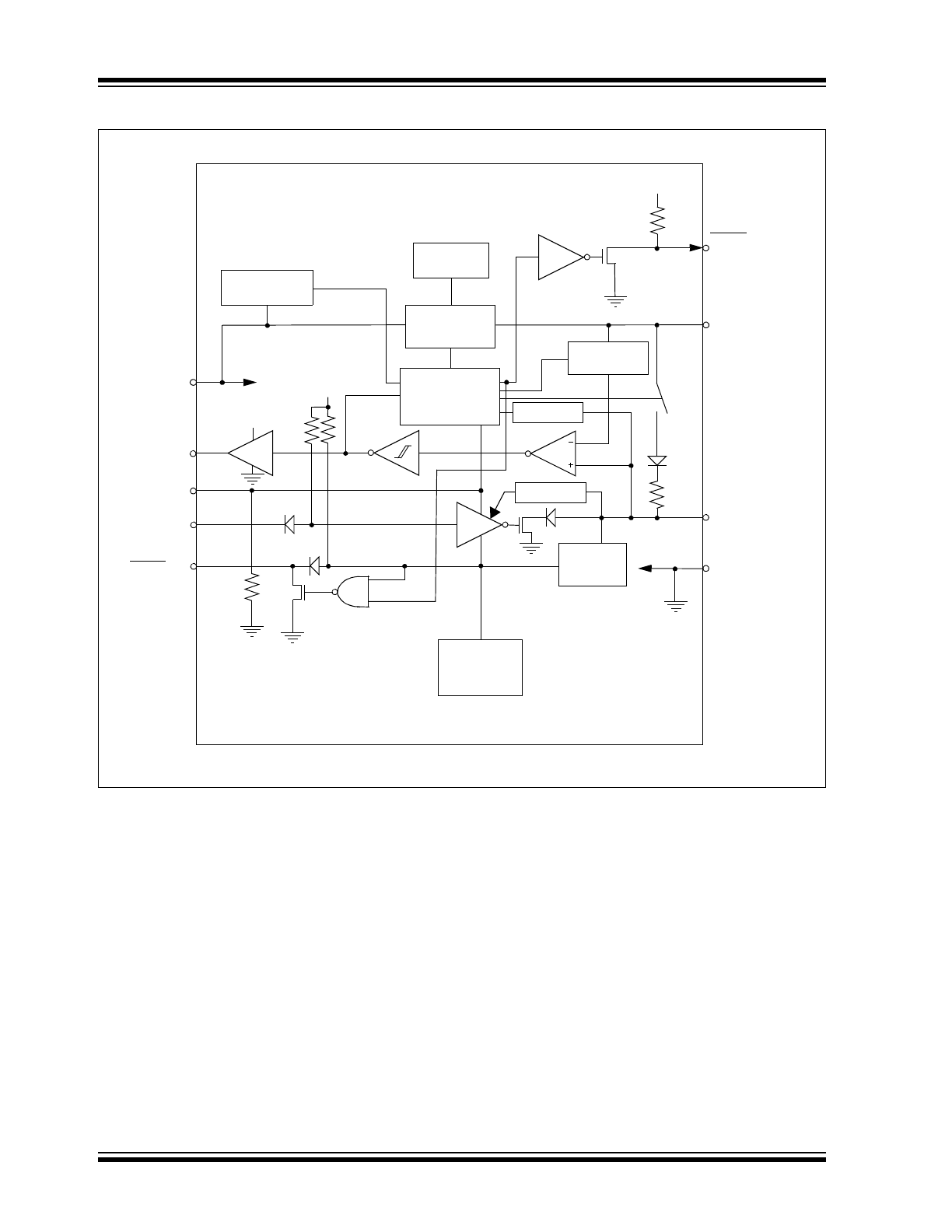
MCP2021A/2A Block Diagram
Internal Circuits
V
REG
FAULT/T
XE
R
XD
T
XD
CS/LWAKE
Bus Wake-Up
Slope Control
V
REG
4.2V
V
REG
RESET
(MCP2022A only)
V
BB
L
BUS
V
SS
~ 30 k
Short Circuit
Protection
Thermal
Protection
Voltage
Regulator
Wake-Up Logic
and
Power Control
Ratiometric
Reference
Bus
Dominant
Timer
Thermal and
Short Circuit
Protection
2012-2014 Microchip Technology Inc.
DS20002298C-page 3
MCP2021A/2A
1.0
DEVICE OVERVIEW
The MCP2021A/2A devices provide a physical
interface between a microcontroller and a LIN
half-duplex bus. They are intended for automotive and
industrial applications with serial bus baud rates up to
20 kBaud. These devices will translate the CMOS/TTL
logic levels to LIN logic levels and vice versa.
The MCP2021A/2A offer optimum EMI and ESD
performance and can withstand high voltage on the LIN
bus. The devices support two low-power modes to
meet automotive industry power consumption
requirements. The MCP2021A/2A also provide a +5V
or 3.3V regulated power output at 70 mA.
1.1
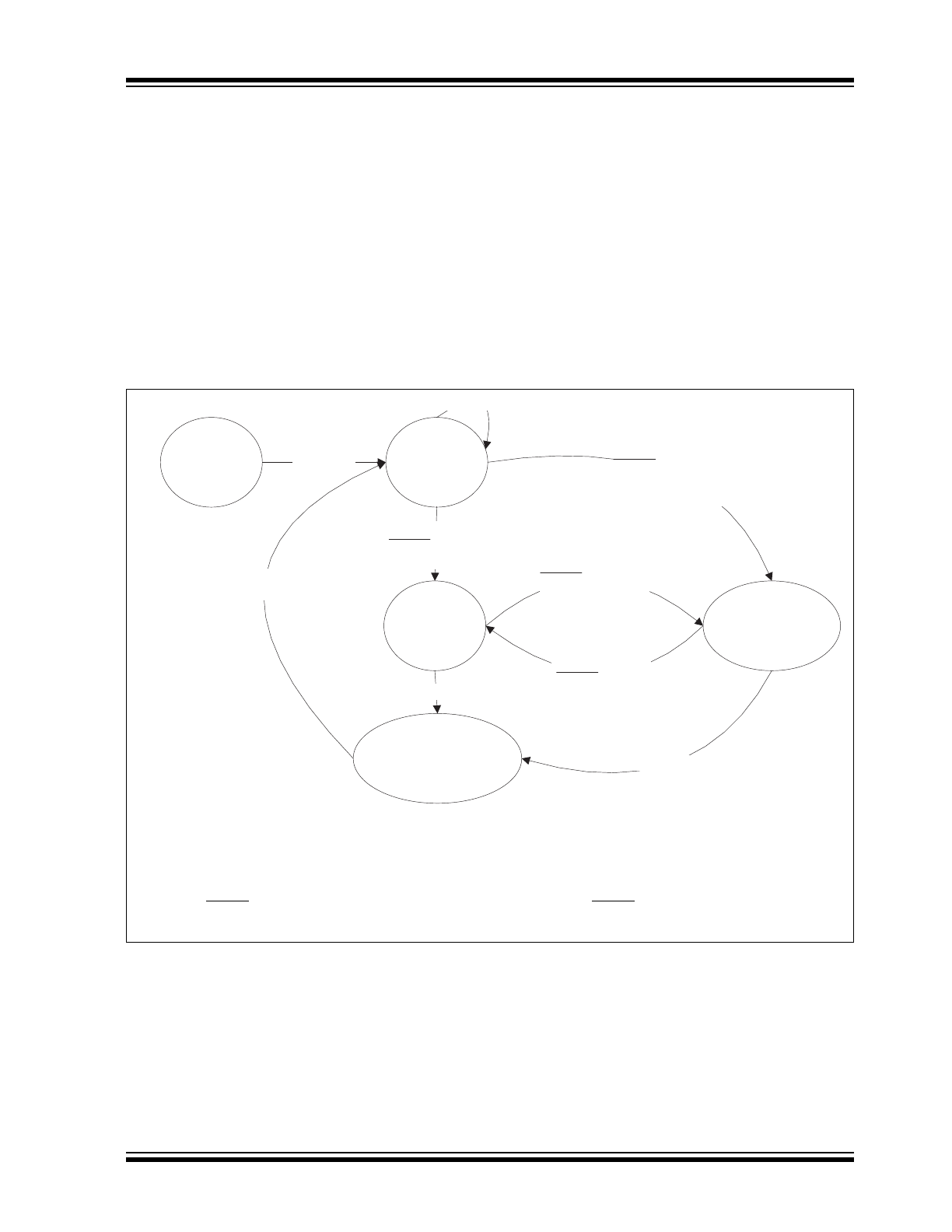
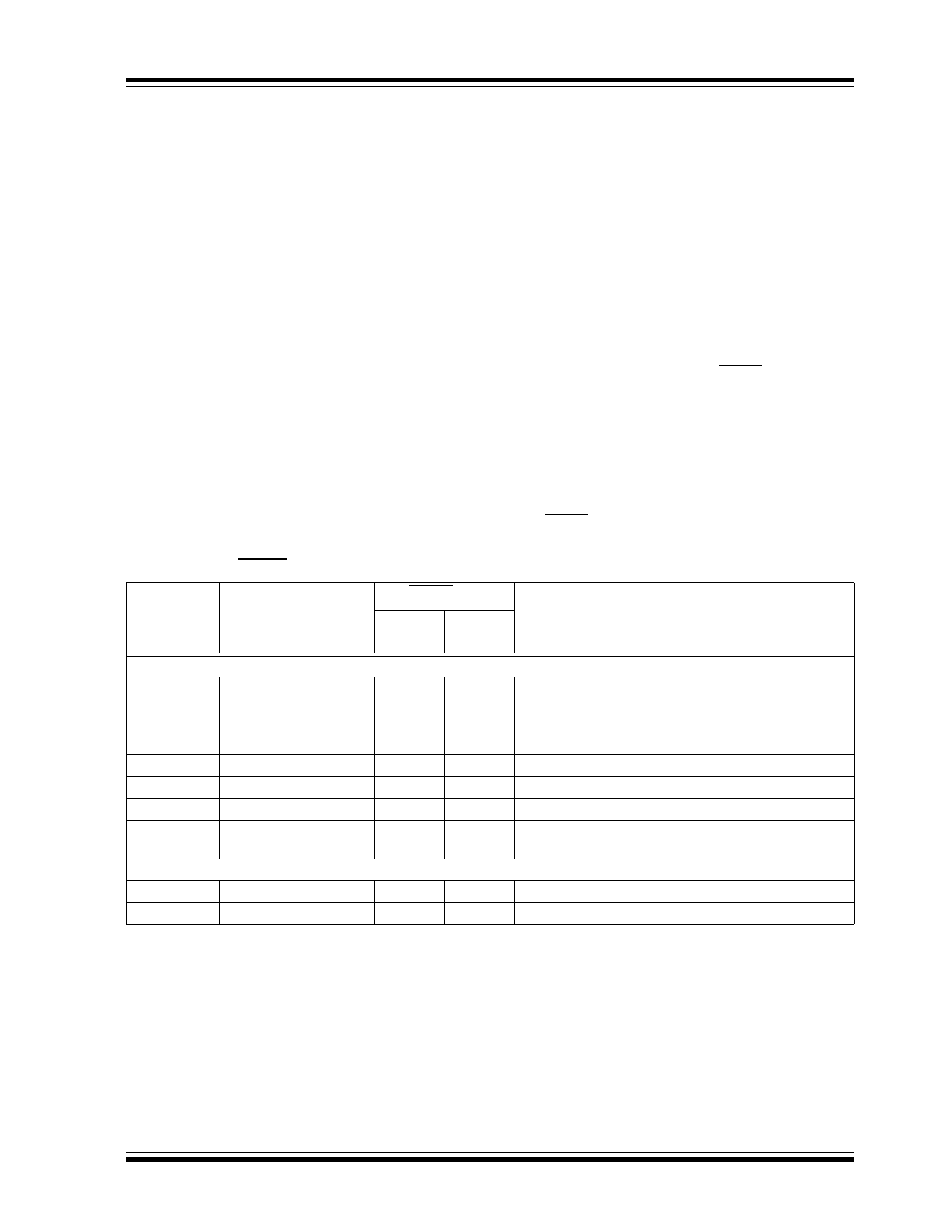
Modes of Operation
The MCP2021A/2A work in five modes: Power-On
Reset, Power-Down, Ready, Operation and
Transmitter Off. For an overview of all operational
modes, please refer to
Table 1-1
. For the operational
mode transition, please refer to
Figure 1-1
.
FIGURE 1-1:
STATE DIAGRAM
Note 1:
VREG_OK: Regulator Output Voltage > 0.8V
REG
_
NOM
.
2:
If the voltage on pin V
BB
falls below V
OFF
, the device will enter Power-On Reset mode from all other
modes, which is not shown in the figure.
3:
FAULT/T
XE
= 1 represents input high and no fault conditions. FAULT/T
XE
= 0 represents input low or a
fault condition. Refer to
Table 1-5
.
POR
(2)
V
REG
OFF
RX OFF
TX OFF
READY
V
REG
ON
RX ON
TX OFF
TX OFF
V
REG
ON
RX ON
TX OFF
POWER-DOWN
V
REG
OFF
RX OFF
TX OFF
OPERATION
V
REG
ON
RX ON
TX ON
V
BB
> V
ON
CS/LWAKE =
1&
FAULT/T
XE
=
0&
CS/LWAKE =
0
CS/LWAKE =
1 &
FAULT/T
XE
=
1
(3)
&
T
XD
=
1&
VREG_OK =
1
(1)
CS/LWAKE =
1&
FAULT/T
XE
=
1
(3)
&
T
XD
=
1
CS/LWAKE =
1&
FAULT/T
XE
=
0
CS/LWAKE =
0
CS/LWAKE =
1 OR
Voltage Rising Edge on LBUS
CS/LWAKE =
0

MCP2021A/2A
DS20002298C-page 4
2012-2014 Microchip Technology Inc.
1.1.1
POWER-ON RESET MODE
Upon application of V
BB
or whenever the voltage on
V
BB
is below the threshold of regulator turn-off voltage
V
OFF
(typically 4.50V), the device enters Power-On
Reset (POR) mode. During this mode, the device
maintains the digital section in a Reset mode and waits
until the voltage on the V
BB
pin rises above the
threshold of regulator turn-on voltage V
ON
(typically
5.75V) to enter Ready mode. In Power-On Reset
mode, the LIN physical layer and voltage regulator are
disabled and the RESET output (MCP2022A only) is
forced to low.
1.1.2
READY MODE
The device enters Ready mode from POR mode after
the voltage on V
BB
rises above the threshold of
regulator turn-on voltage V
ON
or from Power-Down
mode when a remote or local wake-up event happens.
Upon entering Ready mode, the voltage regulator and
the receiver section of the transceiver are powered up.
The transmitter remains in an off state. The device is
ready to receive data but not to transmit. In order to
minimize the power consumption, the regulator
operates in a reduced-power mode. It has a lower
GBW product and it is thus slower. However, the 70 mA
drive capability is unchanged.
The device stays in Ready mode until the output of the
voltage regulator has stabilized and the CS/LWAKE pin
is high (‘1’).
1.1.3
OPERATION MODE
If V
REG
is OK (V
REG
> 0.8 V
REG
_
NORM
) and the
CS/LWAKE, FAULT/TXE and T
XD
pins are high, the
part enters Operation mode from either Ready or
Transmitter Off mode.
In this mode, all internal modules are operational. The
internal pull-up resistor between L
BUS
and V
BB
is
connected only in this mode.
The device goes into Power-Down mode at the falling
edge on CS/LWAKE or into Transmitter Off mode at the
falling edge on FAULT/T
XE
while CS/LWAKE stays
high.
1.1.4
TRANSMITTER OFF MODE
In Transmitter Off mode, the receiver is enabled but the
L
BUS
transmitter is off. It is a lower power mode.
In order to minimize power consumption, the regulator
operates in a reduced-power mode. It has a lower
GBW product and it is thus slower. However, the 70 mA
drive capability is unchanged.
The transmitter may be re-enabled whenever the
FAULT/T
XE
signal returns high, by removing the
internal fault condition and by driving FAULT/T
XE
high.
The transmitter will not be enabled even if the
FAULT/T
XE
pin is brought high externally, when the
internal fault is still present. However, externally forcing
the FAULT/T
XE
high while the internal fault is still
present should be avoided, since this will induce high
current and power dissipation in the FAULT/T
XE
pin.
The transmitter is also turned off whenever the voltage
regulator is unstable or recovering from a fault. This
prevents unwanted disruption of the bus during times of
uncertain operation.
1.1.5
POWER-DOWN MODE
In Power-Down mode, the transceiver and the voltage
regulator are both off. Only the bus wake-up section
and the CS/LWAKE pin wake-up circuits are in
operation. This is the lowest power mode.
If any bus activity (e.g., a Break character) occurs
during Power-Down mode, the device will immediately
enter Ready mode and enable the voltage regulator.
Then, once the regulator output has stabilized
(approximately 0.3 ms to 1.2 ms), it goes into
Operation mode. Refer to
Section 1.1.6 “Remote
Wake-Up”
.
The part will also enter Ready mode from Power-Down
mode, followed by the Operation mode, if the
CS/LWAKE pin becomes active high (‘1’).
1.1.6
REMOTE WAKE-UP
The Remote Wake-Up sub-module observes the L
BUS
in order to detect bus activity. In Power-Down mode,
normal LIN recessive/dominant threshold is disabled
and the LIN bus wake-up voltage threshold V
WK
(
LBUS
)
is used to detect bus activities. Bus activity is detected
when the voltage on the L
BUS
falls below the LIN bus
wake-up voltage threshold V
WK
(
LBUS
) (approximately
3.5V) for at least t
BDB
(a typical duration of 80 µs)
followed by a rising edge. Such a condition causes the
device to leave Power-Down mode.
2012-2014 Microchip Technology Inc.
DS20002298C-page 5
MCP2021A/2A
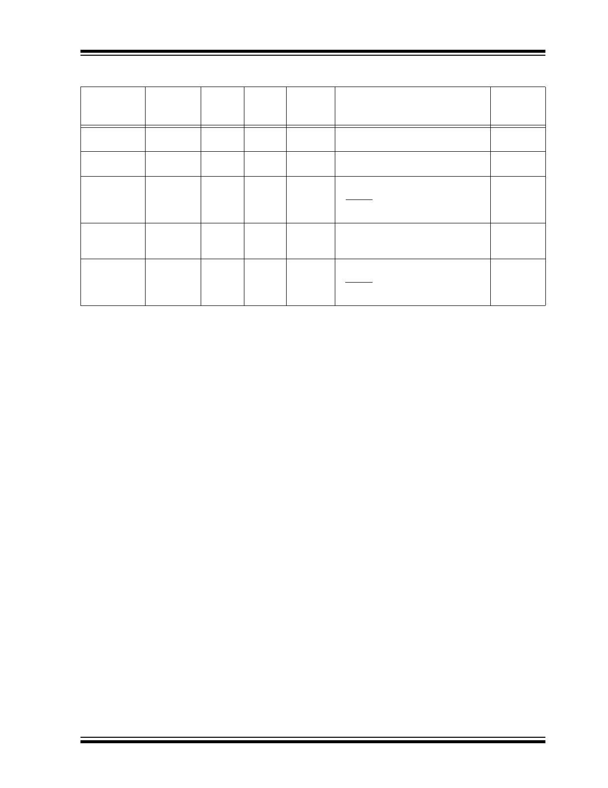
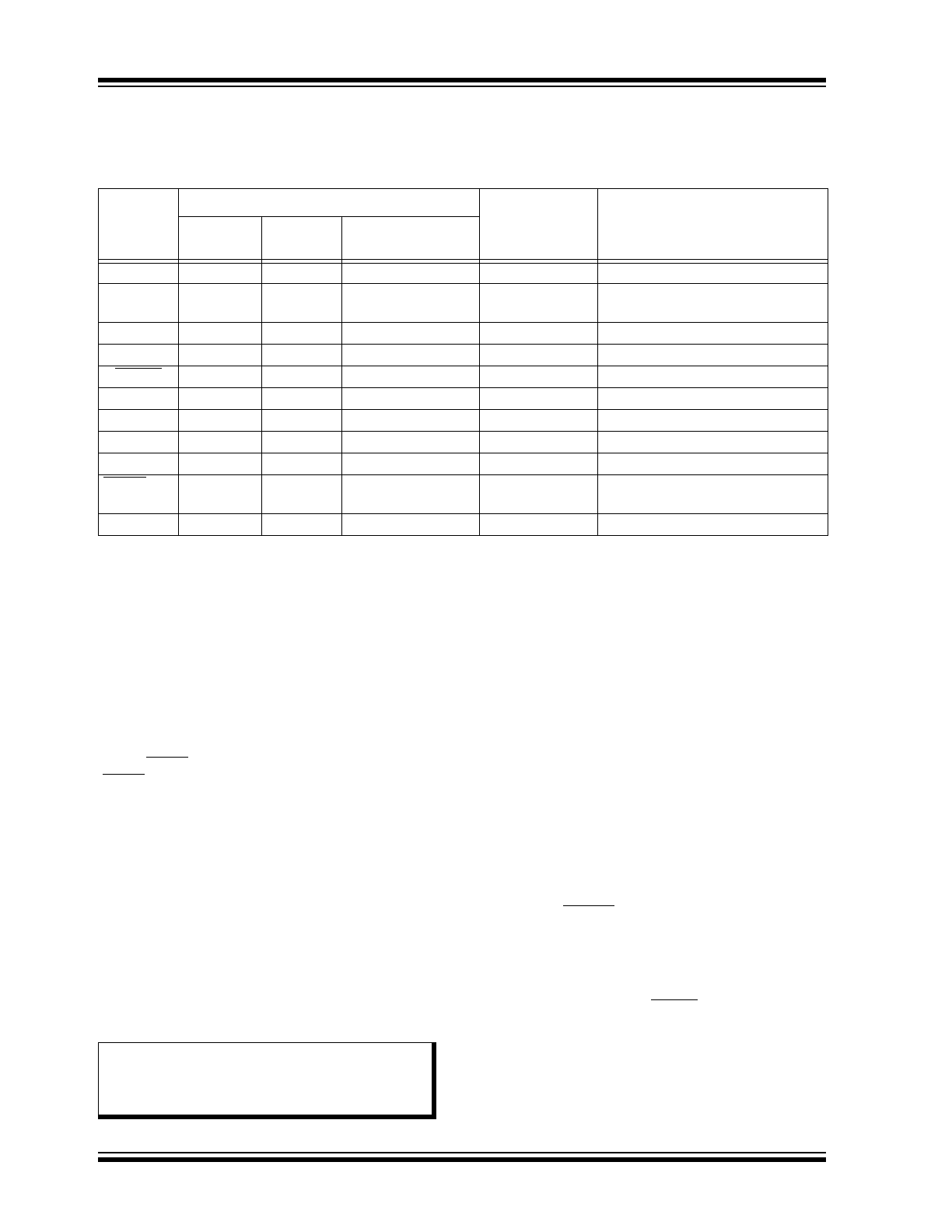
TABLE 1-1:
OVERVIEW OF OPERATIONAL MODES
State
Transmitter Receiver
Internal
Wake
Module
Voltage
Regulator
Operation
Comments
POR
OFF
OFF
OFF
OFF
Proceed to Ready mode after
V
BB
> V
ON
Ready
OFF
ON
OFF
ON
If CS/LWAKE is high, then proceed to
Operation or Transmitter Off mode.
Bus Off
state
Operation
ON
ON
OFF
ON
If CS/LWAKE is low, then proceed to
Power-Down mode.
If FAULT/T
XE
is low, then proceed to
Transmitter Off mode.
Normal
Operation
mode
Power-Down
OFF
OFF
ON
Activity
Detect
OFF
On LIN bus rising edge or CS/LWAKE
high level, go to Ready mode.
Lowest
power mode
Transmitter Off
OFF
ON
OFF
ON
If CS/LWAKE is low, then proceed to
Power-Down mode.
If FAULT/T
XE
is high, then proceed to
Operation mode.
Bus Off
state,
lower power
mode
MCP2021A/2A
DS20002298C-page 6
2012-2014 Microchip Technology Inc.
1.2
Pin Descriptions
The descriptions of the pins are listed in
Table 1-2
.
1.2.1
RECEIVE DATA OUTPUT (R
XD
)
Receive Data Output pin. The R
XD
pin is a standard
CMOS output pin and it follows the state of the L
BUS
pin.
1.2.2
CHIP SELECT AND LOCAL
WAKE-UP INPUT (CS/LWAKE)
Chip Select and Local Wake-up Input pin (TTL level,
high-voltage tolerant). This pin controls the device state
transition. Refer to
Figure 1-1
.
If CS/LWAKE = 1, the device can work in Operation
mode (FAULT/T
XE
= 1) or in Transmitter Off mode
(FAULT/T
XE
= 0). If CS/LWAKE = 0, the device can
work in Power-Down mode or in Ready mode.
An internal pull-down resistor will keep the CS/LWAKE
pin low to ensure that no disruptive data will be present
on the bus while the microcontroller is executing a
Power-On Reset and I/O initialization sequence. When
CS/LWAKE is ‘1’, a weak pull-down (~600 kΩ) is used
to reduce current. When CS/LWAKE is ‘0’, a stronger
pull-down (~300 kΩ) is used to maintain the logic level.
This pin may also be used as a local wake-up input
(see
Figure 1-1
). The microcontroller will set the I/O pin
to control the CS/LWAKE. An external switch or
another source can then wake up both the transceiver
and the microcontroller.
1.2.3
POWER OUTPUT (V
REG
)
Positive Supply Voltage Regulator Output pin. An
on-chip LDO gives +5.0 or +3.3V at 70 mA regulated
voltage on this pin.
1.2.4
TRANSMIT DATA INPUT (T
XD
)
Transmit Data Input pin (TTL level, HV-compliant,
adaptive pull-up). The transmitter reads the data
stream on the T
XD
pin and sends it to the LIN bus. The
L
BUS
pin is low (dominant) when T
XD
is low and high
(recessive) when T
XD
is high.
T
XD
is internally pulled up to approximately 4.2V. When
T
XD
is ‘0’, a weak pull-up (~900 kΩ) is used to reduce
current. When T
XD
is ‘1’, a stronger pull-up (~300 kΩ)
is used to maintain the logic level. A series
reverse-blocking diode allows applying T
XD
input
voltages greater than the internally generated 4.2V and
renders the T
XD
pin HV-compliant up to 30V (see
MCP2021A/2A Block Diagram
).
1.2.5
RESET (MCP2022A ONLY)
RESET output pin. This pin is open-drain with ~90 kΩ
pull-up to V
REG
. It indicates the internal voltage has
reached a valid, stable level. As long as the internal
voltage is valid (above 0.8 V
REG
), this pin will remain
high (‘1’); otherwise, the RESET pin switches to low
(‘0’).
1.2.6
NO CONNECTION (NC)
No internal connection.
TABLE 1-2:
PIN FUNCTION TABLE
Pin Name
Pin Number
Pin Type
Description
8-lead
PDIP, SOIC
4x4 DFN
14-lead
PDIP, SOIC, TSSOP
R
XD
1
1
1
Output
Receive Data Output
CS/LWAKE
2
2
2
TTL Input,
HV-tolerant
Chip Select and Local Wake-up
Input
V
REG
3
3
3
Output
Voltage Regulator Output
T
XD
4
4
4
Input, HV-tolerant Transmit Data Input
RESET
—
—
5
Output
Reset Output
NC
—
—
6–10
—
No Connection
V
SS
5
5
11
Power
Ground
L
BUS
6
6
12
I/O, HV
LIN Bus
V
BB
7
7
13
Power
Battery
FAULT/T
XE
8
8
14
I/O, HV-tolerant
Fault Detect Output/Transmitter
Enable Input
EP
—
9
—
—
Exposed Thermal Pad
Note:
CS/LWAKE should NOT be tied directly to
the V
REG
pin as this could force the
MCP2021A/2A into Operation mode
before the microcontroller is initialized.
2012-2014 Microchip Technology Inc.
DS20002298C-page 7
MCP2021A/2A
1.2.7
GROUND (V
SS
)
Ground pin.
1.2.8
LIN BUS (L
BUS
)
LIN Bus pin. L
BUS
is a bidirectional LIN bus interface
pin and is controlled by the signal T
XD
. It has an open
collector output with a current limitation. To reduce
electromagnetic emission, the slopes during signal
changes are controlled and the L
BUS
pin has
corner-rounding control for both falling and rising
edges.
The internal LIN receiver observes the activities on the
LIN bus and generates the output signal R
XD
that
follows the state of the L
BUS
. A 1
st
degree 160 kHz
low-pass input filter optimizes electromagnetic
immunity.
1.2.9
BATTERY POSITIVE SUPPLY
VOLTAGE (V
BB
)
Battery Positive Supply Voltage pin. An external diode
is connected in series to prevent the device from being
reversely powered (refer to
Figure 1-7
).
1.2.10
FAULT DETECT
OUTPUT/TRANSMITTER ENABLE
INPUT (FAULT/T
XE
)
Fault Detect Output/Transmitter Enable Input pin. The
output section is HV-tolerant open-drain (up to 30V).
The input section is identical to the T
XD
section (TTL
level, HV-compliant, adaptive pull-up). The internal
pull-up resistor may be too weak for some applications.
We recommend adding a 10 k
external pull-up
resistor to ensure a logic high level. Its state is defined
as shown in
Table 1-5
. The device is placed in
Transmitter Off mode whenever this pin is low (‘0’),
either from an internal fault condition or by external
drive.
If CS/LWAKE is high (‘1’), the FAULT/T
XE
signals a
mismatch between the T
XD
input and the L
BUS
level.
This can be used to detect a bus contention. Since the
bus exhibits a propagation delay, the sampling of the
internal compare is debounced to eliminate false faults.
After the device wakes up, the FAULT/T
XE
indicates
what wakes the device if CS/LWAKE remains low (‘0’)
(refer to
Table 1-5
).
The FAULT/T
XE
pin sampled at a rate faster than every
10 µs.
TABLE 1-3:
FAULT/T
XE
TRUTH TABLE
T
XD
In
R
XD
Out
LIN
BUS
I/O
Thermal
Override
FAULT/T
XE
Definition
External
Input
Driven
Output
CS = 1
L
H
V
BB
OFF
H
L
FAULT
, T
XD
driven low, L
BUS
shorted to V
BB
(
Note 1
)
or L
BUS
/T
XD
permanent dominant detected and Trans-
mit time-out shutdown.
H
H
V
BB
OFF
H
H
OK
L
L
GND
OFF
H
H
OK
H
L
GND
OFF
H
H
OK
, data is being received from L
BUS
x
x
V
BB
ON
H
L
FAULT
, Transceiver in thermal shutdown
x
x
V
BB
x
L
x
NO FAULT
, the CPU is commanding the transceiver
to turn off the transmitter driver
CS = 0
x
x
x
x
x
L
Wake-up from LIN bus activity
x
x
x
x
x
H
Wake-up from POR
Legend:
x = Don’t care
Note 1:
The FAULT/T
XE
is valid after approximately 25 µs after the T
XD
falling edge. This is to eliminate false fault
reporting during bus propagation delays.
MCP2021A/2A
DS20002298C-page 8
2012-2014 Microchip Technology Inc.
1.3
Fail-Safe Features
1.3.1
GENERAL FAIL-SAFE FEATURES
• An internal pull-down resistor on CS/LWAKE pin
disables the transmitter if the pin is floating.
• An internal pull-up resistor on the T
XD
pin places
T
XD
in high and the L
BUS
in recessive if the T
XD
pin is floating.
• High-impedance and low-leakage current on L
BUS
during loss of power or ground.
• The current limit on L
BUS
protects the transceiver
from being damaged if the pin is shorted to V
BB
.
1.3.2
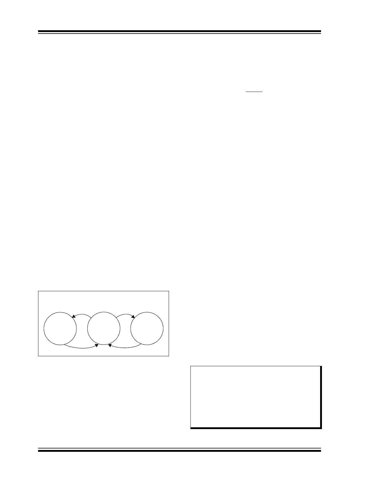
THERMAL PROTECTION
The thermal protection circuit monitors the die
temperature and is able to shut down the
LIN
transmitter and voltage regulator.
There are three causes for a thermal overload. A
thermal shutdown can be triggered by any one, or a
combination of, the following thermal overload
conditions:
• Voltage regulator overload
• LIN bus output overload
• Increase in die temperature due to increase in
environment temperature
The recovery time from the thermal shutdown is equal
to adequate cooling time.
Driving the T
XD
and checking the R
XD
pin make it
possible to determine whether there is a bus contention
(T
XD
= high, R
XD
= low) or a thermal overload
condition (T
XD
= low, R
XD
= high).
FIGURE 1-2:
THERMAL SHUTDOWN
STATE DIAGRAMS
1.3.3
T
XD
/L
BUS
TIME-OUT TIMER
The LIN bus can be driven to a dominant level either
from the T
XD
pin or externally. An internal timer
deactivates the L
BUS
transmitter if a dominant status
(low) on the LIN bus lasts longer than Bus Dominant
Time-out Time, t
TO
(
LIN
) (approximately
20 milliseconds). At the same time, the R
XD
output is
put in recessive (high), FAULT/T
XE
is also driven to low
and the internal LIN pull-up resistor is disconnected.
The timer is reset on any recessive L
BUS
status or POR
mode. The recessive status on L
BUS
can be caused
either by the bus being externally pulled up or by the
T
XD
pin being returned high.
1.4
Internal Voltage Regulator
The MCP2021A/2A have a positive regulator capable
of supplying +5.00 or +3.30 V
DC
±3% at up to 70 mA of
load current over the entire operating temperature
range of -40°C to +125°C. The regulator uses a LDO
design, is short-circuit-protected and will turn the
regulator output off if its output falls below the shutdown
voltage threshold, V
SD
.
With a load current of 70 mA, the minimum input to
output voltage differential required for the output to
remain in regulation is typically +0.5V (+1V maximum
over the full operating temperature range). Quiescent
current is less than 100 µA with a full 70 mA load
current when the input to output voltage differential is
greater than +3.00V.
Regarding the correlation between V
BB
, V
REG
and I
DD
,
please refer to
Figures 1-4
and
1-5
. When the input
voltage (V
BB
) drops below the differential needed to
provide stable regulation, the voltage regulator output,
V
REG
, will track the input down to approximately V
OFF
,
at which point the regulator will turn off the output. This
will allow PIC
®
microcontrollers with internal POR
circuits to generate a clean arming of the POR trip
point. The MCP2021A/2A will then monitor V
BB
and
turn on the regulator when V
BB
is above the threshold
of regulator turn-on voltage, V
ON
.
In Power-Down mode, the V
BB
monitor is turned off.
Under specific ambient temperature and battery
voltage range, the voltage regulator can output as high
as 150 mA current. For current load capability of the
voltage regulator, refer to
Figures 2-8
and
2-9
.
Voltage
Regulator
Shutdown
Operation
Mode
Transmitter
Shutdown
Output
Overload
LIN Bus
Shorted to
V
BB
Temp < SHUTDOWN
TEMP
Temp < SHUTDOWN
TEMP
Note:
The regulator has an overload current limit
of approximately 250 mA. The regulator
output voltage, V
REG
, is monitored. If
output voltage V
REG
is lower than V
SD
, the
voltage regulator will turn off. After a
recovery time of about 3 ms, the V
REG
will
be checked again. If there is no short
circuit (V
REG
> V
SD
), then the voltage
regulator remains on.
2012-2014 Microchip Technology Inc.
DS20002298C-page 9
MCP2021A/2A
The regulator requires an external output bypass
capacitor for stability. See
Figure 2-1
for correct
capacity and ESR for stable operation.
In worst-case scenarios, the ceramic capacitor may
derate by 50%, based on tolerance, voltage and
temperature. Therefore, in order to ensure stability,
ceramic capacitors smaller than 10 µF may require a
small series resistance to meet the ESR requirements,
as shown in
Table 1-4
.
FIGURE 1-3:
VOLTAGE REGULATOR BLOCK DIAGRAM
Note:
A ceramic capacitor of at least 10 µF or a
tantalum capacitor of at least 2.2 µF is
recommended for stability.
TABLE 1-4:
RECOMMENDED SERIES
RESISTANCE FOR CERAMIC
CAPACITORS
Resistance
Capacitor
1
1 µF
0.47
2.2 µF
0.22
4.7 µF
0.1
6.8 µF
Pass
Element
Sampling
Network
Buffer
V
REG
V
BB
V
SS
Fast
Transient
Loop
V
REF
MCP2021A/2A
DS20002298C-page 10
2012-2014 Microchip Technology Inc.
FIGURE 1-4:
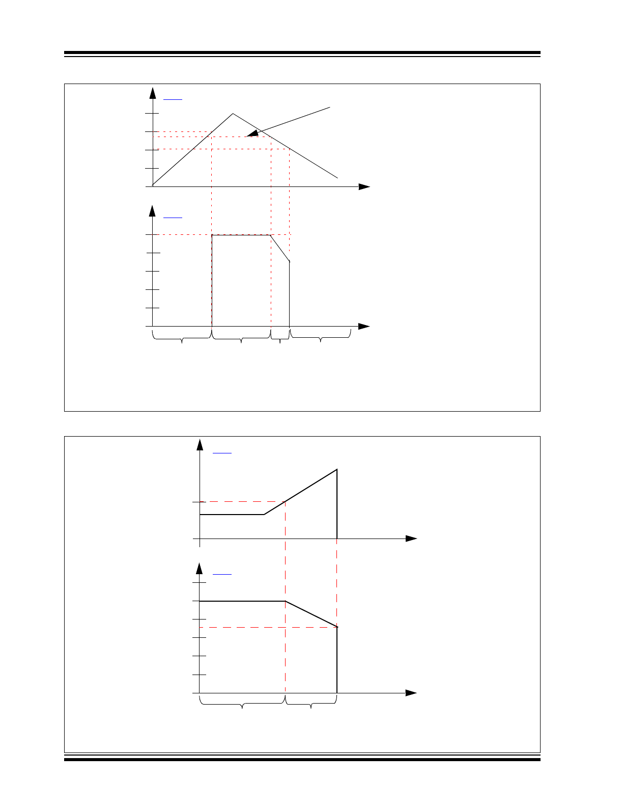
VOLTAGE REGULATOR OUTPUT ON POWER-ON RESET
FIGURE 1-5:
VOLTAGE REGULATOR OUTPUT ON OVERCURRENT PROTECTION
Note 1:
Start-up, V
BB
< V
ON
, regulator off.
2:
V
BB
> V
ON
, regulator on.
3:
V
BB
Minimum V
BB
to maintain regulation.
4:
V
BB
< V
OFF
, regulator will turn off.
5
3
2
0
(1)
(2)
(3)
t
0
t
6
2
8
4
V
BB
V
V
REG
V
1
4
V
ON
V
OFF
Minimum V
BB
to maintain regulation
V
REG
-
NOM
(4)
Note 1:
I
REG
less than l
LIM
, regulator on.
2:
After I
REG
exceeds l
LIM
, the voltage regulator output will be reduced until V
SD
is reached.
V
SD
0
(1)
(2)
t
0
t
l
LIM
I
REG
mA
V
REG
V
V
REG
-
NOM
1
2
3
4
5
6