
©
2007 Microchip Technology Inc.
DS21730F-page 1
MCP201
Features
• Supports baud rates up to 20 Kbaud
• 40V load dump protected
• Wide supply voltage, 6.0 – 18.0V, continuous
- Maximum input voltage of 30V
• Extended Temperature Range: -40°C to +125°C
• Interface to standard USARTs
• Compatible with LIN Spec 1.3
• Local Interconnect Network (LIN) Line pin:
- Internal pull-up resistor and diode
- Protected against ground shorts (LIN pin to
ground)
- Protected against LIN pin loss of ground
- High current drive, 40 mA
≤
I
OL
≤
200 mA
• Automatic thermal shutdown
• On-board Voltage Regulator:
- Output voltage of 5V with ±5% tolerances
over temperature range
- Maximum output current of 50 mA
- Able to drive an external series-pass
transistor for increased current supply
capability
- Internal thermal overload protection
- Internal short-circuit current limit
- External components limited to filter capacitor
only and load capacitor
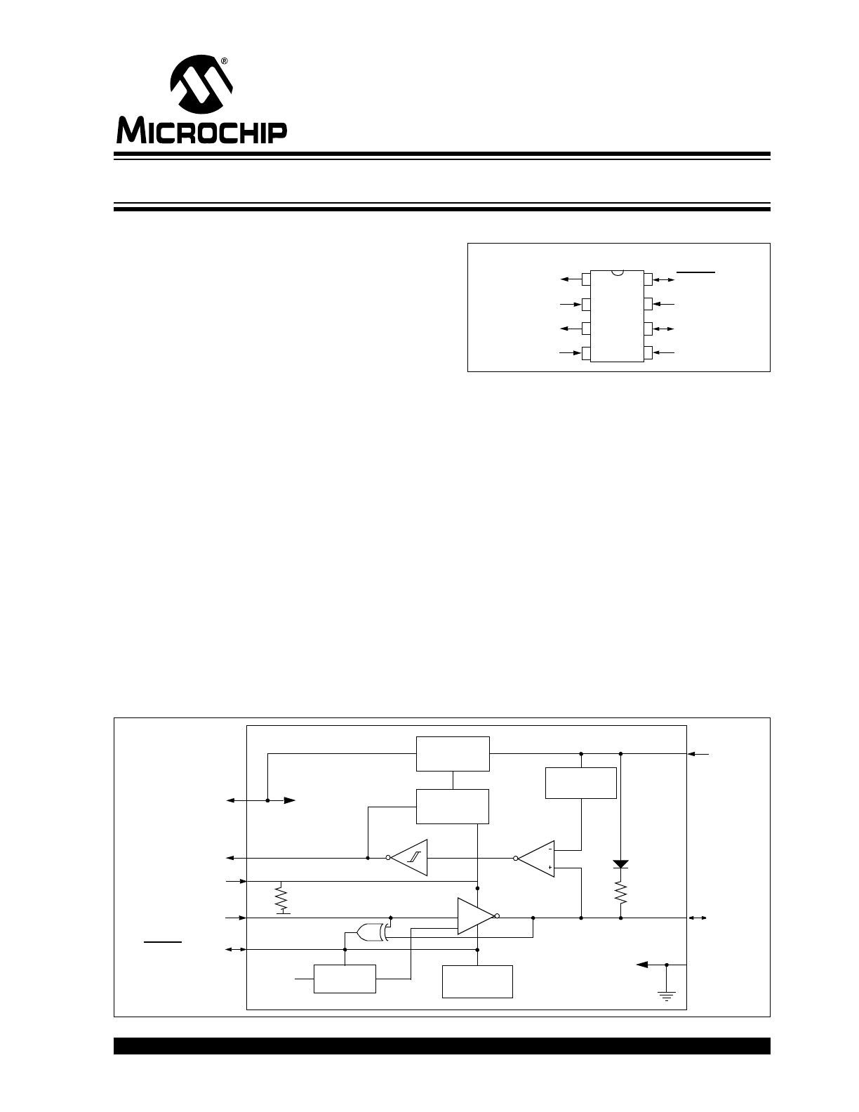
Package Types
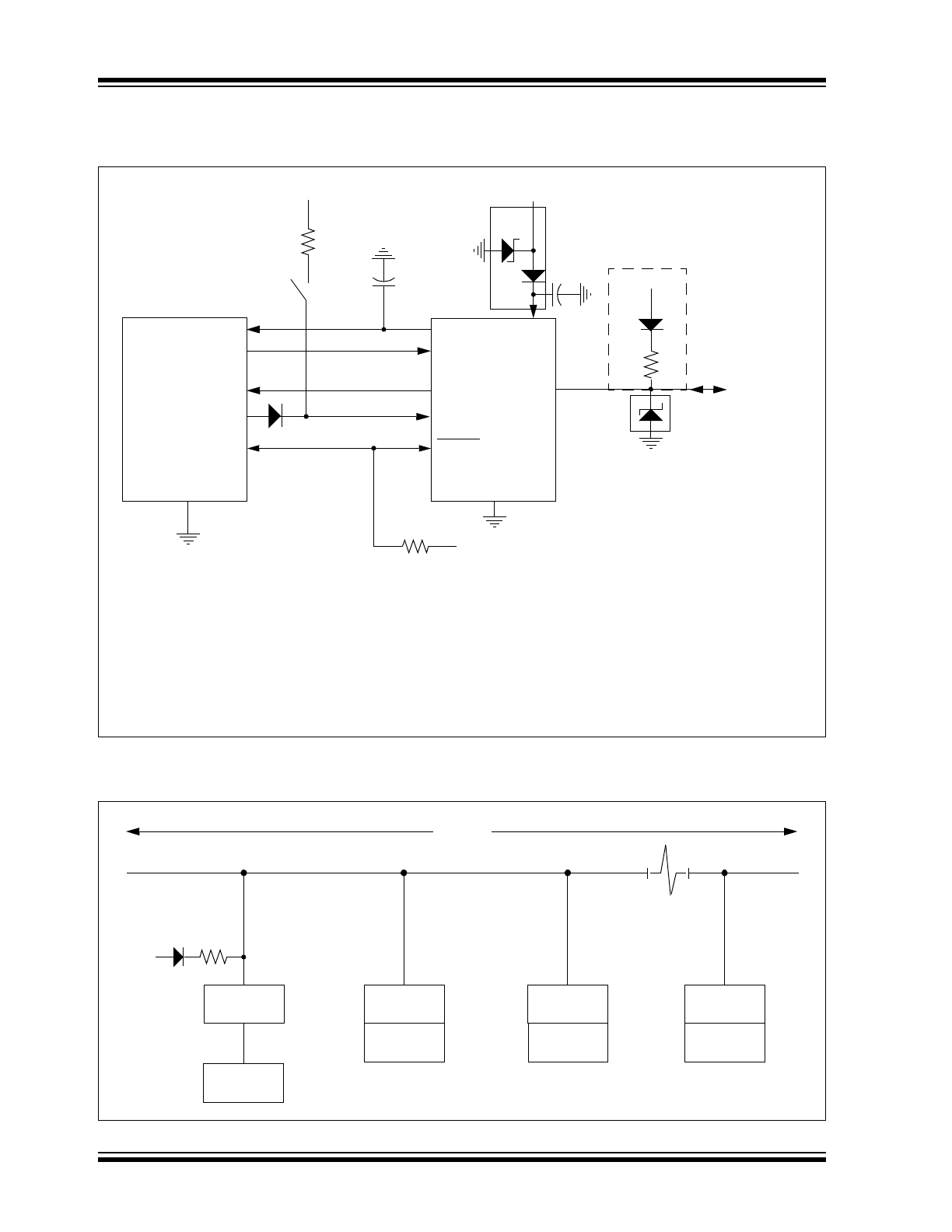
Block Diagram
MCP201
PDIP, SOIC, DFN
8
7
6
5
1
2
3
4
RXD
CS/WAKE
V
REG
TXD
FAULT/SLPS
V
BAT
LIN
V
SS
Voltage
Regulator
Ratiometric
Reference
OC
Thermal
Protection
Internal Circuits
V
REG
FAULT/SLPS
RXD
TXD
V
BAT
LIN
Vss
approx.
CS/WAKE
Wake-Up
Logic
Slope
Control
POR
30 k
Ω
LIN Transceiver with Voltage Regulator

MCP201
DS21730F-page 2
©
2007 Microchip Technology Inc.
NOTES:
©
2007 Microchip Technology Inc.
DS21730F-page 3
MCP201
1.0
DEVICE OVERVIEW
The MCP201 provides a physical interface between a
microcontroller and a LIN half-duplex bus. It is intended
for automotive and industrial applications with serial
bus speeds up to 20 Kbaud.
The MCP201 provides a half-duplex, bidirectional
communications interface between a microcontroller
and the serial network bus. This device will translate
the CMOS/TTL logic levels to LIN level logic, and vice
versa.
The LIN specification 1.3 requires that the transceiver
of all nodes in the system be connected via the LIN pin,
referenced to ground and with a maximum external
termination resistance of 510
Ω
from LIN bus to battery
supply. The 510
Ω
corresponds to 1 Master and 16
Slave nodes.
The MCP201 provides a +5V 50 mA regulated power
output. The regulator uses a LDO design, is short-
circuit-protected and will turn the regulator output off if
it falls below 3.5V. The MCP201 also includes thermal
shutdown protection. The regulator has been specifi-
cally designed to operate in the automotive environ-
ment and will survive reverse battery connections,
+40V load dump transients and double-battery jumps
(see Section 1.6 “Internal Voltage Regulator”).
1.1
Optional External Protection
1.1.1
TRANSIENT VOLTAGE
PROTECTION (LOAD DUMP)
An external 27V transient suppressor (TVS) diode,
between V
BAT
and ground, with a 50
Ω
resistor in series
with the battery supply and the V
BAT
pin, serves to pro-
tect the device from power transients (see Figure 1-2)
and ESD events. While this protection is optional, it
should be considered as good engineering practice.
1.1.2
REVERSE BATTERY PROTECTION
An external reverse-battery-blocking diode can be
used to provide polarity protection (see Figure 1-2).
This protection is optional, but should be considered as
good engineering practice.
1.2
Internal Protection
1.2.1
ESD PROTECTION
For component-level ESD ratings, please refer to the
maximum operation specifications.
1.2.2
GROUND LOSS PROTECTION
The LIN bus specification states that the LIN pin must
transition to the recessive state when ground is
disconnected. Therefore, a loss of ground effectively
forces the LIN line to a hi-impedance level.
1.2.3
THERMAL PROTECTION
The thermal protection circuit monitors the die
temperature and is able to shut down the
LIN
transmitter and voltage regulator. Refer to Table 1-1 for
details.
There are three causes for a thermal overload. A
thermal shut down can be triggered by any one, or a
combination of, the following thermal overload
conditions.
• Voltage regulator overload
• LIN bus output overload
• Increase in die temperature due to increase in
environment temperature
Driving the TXD and checking the RXD pin makes it
possible to determine whether there is a bus contention
(Rx = low, Tx = high) or a thermal overload condition
(Rx = high, Tx = low).
TABLE 1-1:
SOURCES OF THERMAL OVERLOAD
(1,2)
Note:
After recovering from a thermal, bus or
voltage regulator overload condition, the
device will be in the Ready1 mode. In order
to go into Operational mode, the CS/
WAKE pin has to be toggled.
TXD
RXD
Comments
L
H
LIN transmitter shutdown, receiver and voltage regulator active, thermal overload
condition.
H
L
Regulator shutdown, receiver active, bus contention.
Legend: x = Don’t care, L = Low, H = High
Note 1:
LIN transceiver overload current on the LIN pin is 200 mA.
2:
Voltage regulator overload current on voltage regulator greater than 50 mA.
MCP201
DS21730F-page 4
©
2007 Microchip Technology Inc.
1.3
Modes of Operation
For an overview of all operational modes, please refer
to Table 1-2.
1.3.1
POWER-DOWN MODE
In the Power-down mode, the transmitter and the
voltage regulator are both off. Only the receiver section
and the CS/WAKE pin wake-up circuits are in
operation. This is the lowest power mode.
If any bus activity (e.g., a BREAK character) should
occur during Power-down mode, the device will
immediately enable the voltage regulator. Once the
output has stabilized, the device will enter Ready
mode.
The part will enter the Operation mode, if the CS/WAKE
pin should become active-high (‘
1
’).
1.3.2
READY AND READY1 MODES
There are two states for the Ready mode. The only
difference between these states is the transition during
start-up. The state Ready1 mode ensures that the
transition from Ready to Operation mode (once a rising
edge of CS/WAKE) occurs without disrupting bus
traffic.
Immediately upon entering either Ready1 or Ready
mode, the voltage regulator will turn on and provide
power. The transmitter portion of the circuit is off, with
all other circuits (including the receiver) of the MCP201
being fully operational. The LIN pin is kept in a
recessive state.
If a microcontroller is being driven by the voltage
regulator output, it will go through a power-on reset and
initialization sequence. All other circuits, other than the
transmitter, are fully operational. The LIN pin is held in
the recessive state.
The device will stay in Ready mode until the CS/WAKE
pin transitions high (‘
1
’). After CS/WAKE is active, the
transmitter is enabled and the device enters Operation
mode.
The device may only enter Power-down mode after
going through the Operation mode step.
At power-on of the V
BAT
supply pin, the component is
in either Ready or Ready1 mode, waiting for a
CS/WAKE rising edge.
The MCP201 will stay in either mode for 600 µs as the
regulator powers its internal circuitry and waits until the
CS/WAKE pin transitions high. During the 600 µs
delay, the MCP201 will not recognize a CS/WAKE
event. The CS/WAKE transition from low to high should
not occur until after this delay.
• The CS input is edge, not level, sensitive.
• The CS pin is not monitored until approximately
600 µs after V
REG
has stabized.
• The transistion from Ready1 to Ready is made on
the falling edge of CS.
• The transition from Ready mode to Operational
mode is on the rising edge of CS.
1.3.3
OPERATION MODE
In this mode, all internal modules are operational.
The MCP201 will go into Power-down mode on the
falling edge of CS/WAKE.
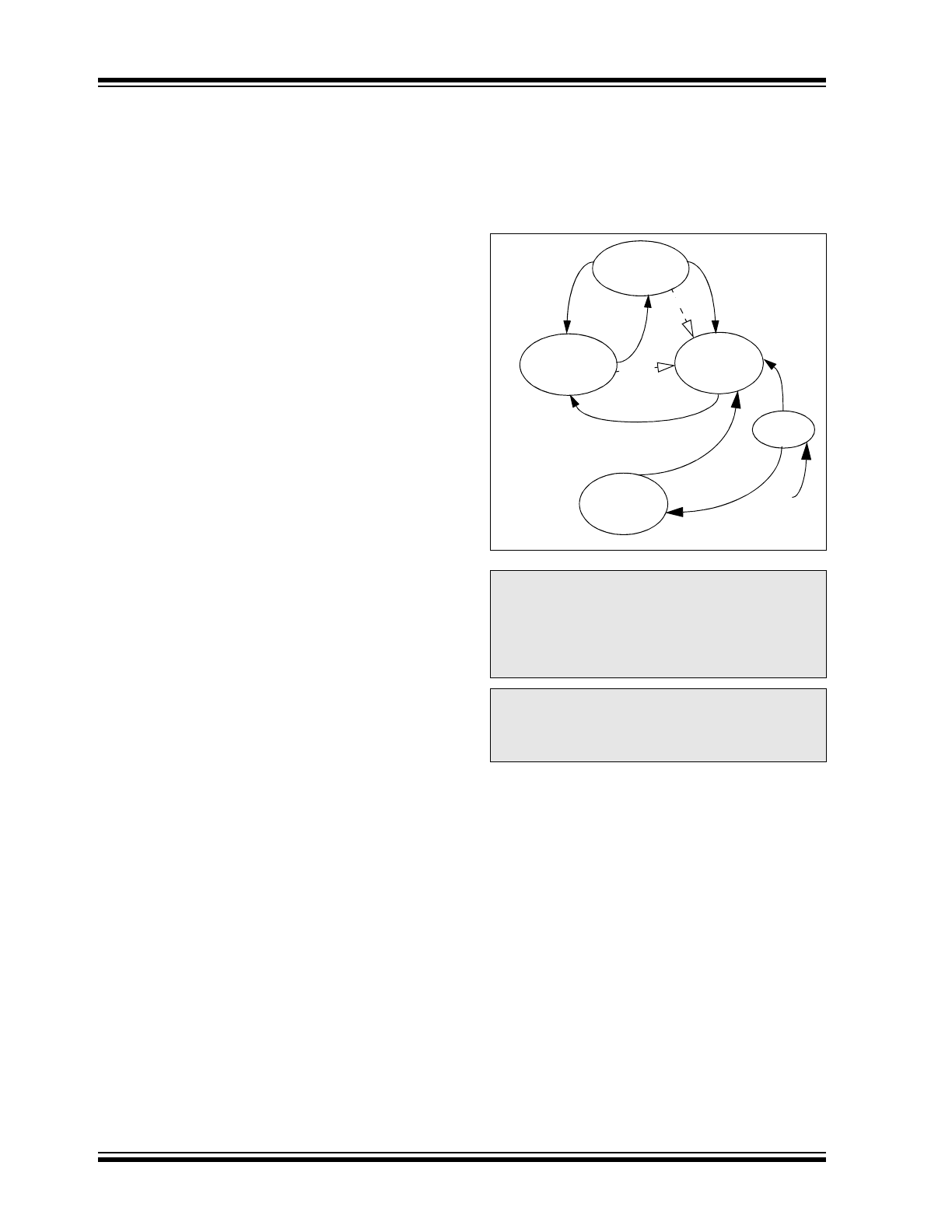
FIGURE 1-1:
OPERATIONAL MODES
STATE DIAGRAMS
1.3.4
DESCRIPTION OF BROWNOUT
CONDITIONS
As V
BAT
decreases V
REG
is regulated to 5.0 VDC (see
V
REG
in Section 2.2 “DC Specifications”) while V
BAT
is greater than 5.5 - 6.0 VDC.
As V
BAT
decreases further V
REG
tracks V
BAT
(V
REG
=
V
BAT
- (0.5 to 1.0) VDC.
The MCP201 monitors V
REG
and as long as V
REG
does
not fall below V
SD
(see V
SD
in Section 2.2 “DC Spec-
ifications”), V
REG
will remain powered.
As V
BAT
increases V
REG
will continue to track V
BAT
until V
REG
reaches 5.0 VDC.
If V
REG
falls below V
SD
, V
REG
is turned off and the
MCP201 powers itself down.
The MCP201 will remain powered down until V
BAT
increases above V
ON
(see V
ON
in Section 2.2 “DC
Specifications”.
Note:
After power-on, CS will not be sampled
until V
REG
has stabized and an additional
600 µs has elapsed. The microcontroller
should toggle CS approximately 1mS after
RESET to ensure that CS will be recog-
nized.
Note:
While the MCP201 is in shutdown, TXD
should not be actively driven high. If TXD
is driven high actively, it may power
internal logic.
Operation
Mode
Power-down
Mode
Ready
Mode
Bus Activity
CS/WAKE = true
CS/WAKE = true
POR
CS/WAKE = false
Ready1
Mode
CS/WAKE = true
CS/WAKE = false
C
S
/W
AK
E =
f
a
ls
e
Start
FLT
FLT
©
2007 Microchip Technology Inc.
DS21730F-page 5
MCP201
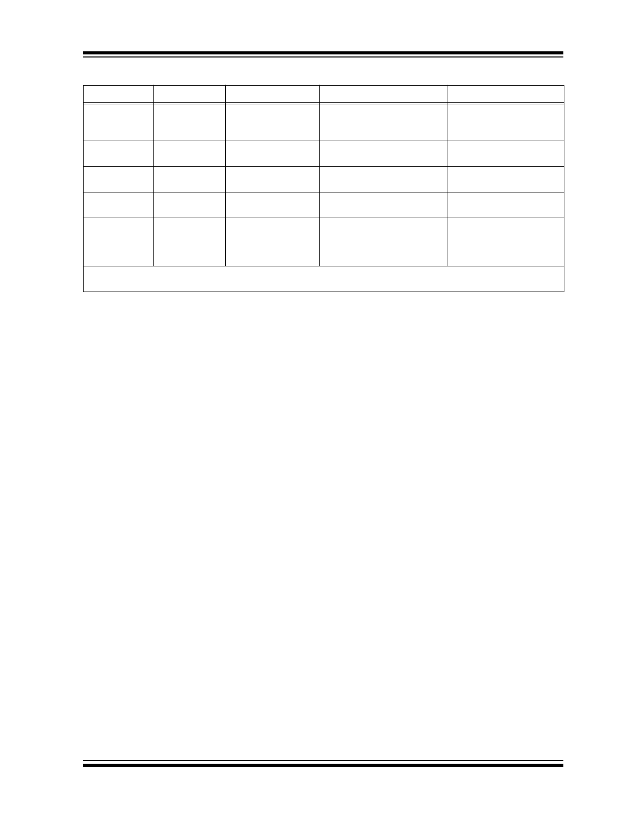
TABLE 1-2:
OVERVIEW OF OPERATIONAL MODES
State
Transmitter
Voltage Regulator
Operation
Comments
POR
OFF
OFF
Read CS/WAKE.
If low, then READY.
If high, READY1 mode.
Sample FAULT/SLPS and
select slope
Ready
OFF
ON
If CS/WAKE rising edge, then
Operation mode.
Bus Off state
Ready1
OFF
ON
If CS/WAKE falling edge,
then READY mode.
Bus Off state
Operation
ON
ON
If CS/WAKE falling edge,
then Power down.
Normal Operation mode
Power-down
OFF
OFF
On LIN bus falling, go to
READY mode.
On CS/WAKE rising edge, go
to Operational mode
Low-Power mode
Note:
After power-on, CS will not be sampled until V
REG
has stabized and an additional 600 µs has elapsed. The
microcontroller should toggle CS approximately 1mS after RESET to ensure that CS will be recognized.
MCP201
DS21730F-page 6
©
2007 Microchip Technology Inc.
1.4
Typical Applications
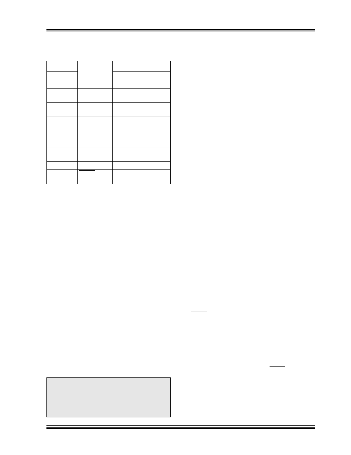
FIGURE 1-2:
TYPICAL MCP201 APPLICATION
(1,2)
FIGURE 1-3:
TYPICAL LIN NETWORK CONFIGURATION
LIN bus
D2
(4)
V
BAT
LIN
V
REG
TXD
RXD
V
SS
V
DD
V
SS
TXD
RXD
+5V
PIC
®
+12V
10 uF
C
G
CS/WAKE
I/O
FAULT/SLPS
I/O
27V
1 k
Ω
+12V
Master Node Only
+12V
10 k
Ω
WAKE-UP
V
REG
or V
SS
100 k
Ω
Optional components
(5)
Optional components
MCP201
C
F
D1
(3)
Note 1: The load capacitor, C
G
, should be a ceramic or tantalum rated for extended temperatures and be in
the range of 1.0 - 22 µF with an ESR 0.4
Ω
- 5
Ω
.
.
2: C
F
if the filter capacitor for the external voltage supply.
3: This diode is only needed if CS/WAKE is connected to 12V supply.
4: Transient suppressor diode. Vclamp L = 40V.
5: These components are for load dump protection.
24V
MCU
LIN bus
MCP201
Master
µC
1 k
Ω
V
BAT
Slave 1
µC
Slave 2
µC
Slave n <16
µC
40m
+ Return
LIN bus
LIN bus
MCP201
LIN bus
MCP201
LIN bus
MCP201
©
2007 Microchip Technology Inc.
DS21730F-page 7
MCP201
1.5
Pin Descriptions
TABLE 1-3:
MCP201 PINOUT OVERVIEW
1.5.1
RECEIVE DATA OUTPUT (RXD)
The Receive Data Output pin is a standard CMOS
output and follows the state of the LIN pin.
The LIN receiver monitors the state of the LIN pin and
generates the output signal RXD.
1.5.2
CS/WAKE
Chip Select Input pin. This pin controls whether the part
goes into READY1 or READY mode at power-up. The
internal pull-down resistor will keep the CS/WAKE pin
low. This is done to ensure that no disruptive data will
be present on the bus while the microcontroller is
executing a Power-on Reset and I/O initialization
sequence. The pin must see a low-to-high transition to
activate the transmitter.
After CS/WAKE transitions to ‘
1
’, the transmitter is
enabled. If CS/WAKE = ‘
0
’, the device is in Ready1
mode on power-up or in Low-Power mode. In Low-
Power mode, the voltage regulator is shut down, the
transmitter driver is disabled and the receiver logic is
enabled.
An external switch (see Figure 1-2) can then wake up
both the transceiver and the microcontroller. An
external-blocking diode and current-limiting resistor are
necessary to protect the microcontroller I/O pin.
1.5.3
POWER OUTPUT (V
REG
)
Positive Supply Voltage Regulator Output pin.
1.5.4
TRANSMIT DATA INPUT (TXD)
The Transmit Data Input pin has an internal pull-up to
V
REG
. The LIN pin is low (dominant) when TXD is low,
and high (recessive) when TXD is high.
In case the thermal protection detects an over-temper-
ature condition while the signal TXD is low, the
transmitter is shutdown. The recovery from the thermal
shutdown is equal to adequate cooling time.
1.5.5
GROUND (V
SS
)
Ground pin.
1.5.6
LIN
The bidirectional LIN bus Interface pin is the driver unit
for the LIN pin and is controlled by the signal TXD. LIN
has an open collector output with a current limitation.
To reduce EMI, the edges during the signal changes
are slope-controlled.
1.5.7
BATTERY (V
BAT
)
Battery Positive Supply Voltage pin. This pin is also the
input for the internal voltage regulator.
1.5.8
FAULT/SLPS
FAULT Detect Output, Slope Select Input.
This pin is usually in Output mode. Its state is defined
as shown in Table 1-5.
The state of this pin is internally sampled during power-
on of V
BAT
. Once V
BAT
has reached a stable level,
(approximately 6 VDC) and V
REG
is stable at 4.75 to
5.25 VDC, the state of this pin selects which slew rate
profile to apply to the LIN output. It is only during this
time that the pin is used as an input (the output driver
is off during this time). The slope will stay selected until
the next V
BAT
power-off/power-on sequence, regard-
less of any power-down, wake-up or SLEEP events.
Only a V
BAT
rising state will cause a sampling of the
FAULT/SLPS pin. The Slope selection will be made
irrespective of the state of any other pin.
The FAULT/SLPS pin is connected to either V
REG
or
V
SS
through a resistor (approximately 100 k
Ω
) to make
the slope selection. This large resistance allows the
FAULT indication function to overdrive the resistor in
normal operation mode.
If the FAULT/SLPS is high (‘
1
’), the normal slope shap-
ing is selected (dv/dt = 2 V/µs). If FAULT/SLPS is low
(‘
0
’) during this time, the alternate slope-shaping is
selected (dv/dt = 4 V/µs). This mode can be used if a
user desires to run at a faster slope. This mode is not
LIN compliant.
Devices
Bond Pad
Name
Function
8-Pin PDIP/
SOIC/DFN
Normal Operation
1
RXD
Receive Data Output
(CMOS output)
2
CS/WAKE
Chip Select (TTL-HV
input)
3
V
REG
Power Output
4
TXD
Transmit Data Input
(TTL)
5
V
SS
Ground
6
LIN
LIN bus (bidirectional-
HV)
7
V
BAT
Battery
8
FAULT/SLPS
Fault Detect Output,
Slope Select Input
Legend: TTL = TTL input buffer,
HV = High Voltage (V
BAT
)
Note:
On POR, the MCP201 enters Ready or
Ready1 mode (see Figure 1-1). In order to
enter Operational mode, the MCP201 has
to see one rising edge on CS/WAKE
600 µs after the voltage regulator reaches
5V.
MCP201
DS21730F-page 8
©
2007 Microchip Technology Inc.
TABLE 1-4:
FAULT / SLPS SLOPE
SELECTION DURING POR
TABLE 1-5:
FAULT / SLPS TRUTH TABLE
1.6
Internal Voltage Regulator
The MCP201 has a low drop-out voltage, positive
regulator capable of supplying 5.00 VDC ±5% at up to
50 mA of load current over the entire operating
temperature range. With a load current of 50 mA, the
minimum input-to-output voltage differential required
for the output to remain in regulation is typically +0.5V
(+1V maximum over the full operating temperature
range). Quiescent current is less than 1.0 mA, with a
full 50 mA load current, when the input-to-output
voltage differential is greater than +2V.
The regulator requires an external output bypass
capacitor for stability. The capacitor should be either a
ceramic or tantalum for stable operation over the
extended temperature range. The compensation
capacitor should range from 1.0 µf – 22 µf and have a
ESR or CSR of 0.4
Ω
– 5.0
Ω
. The input capacitor, C
F
, in
Figure 1.4 should be on the order of 8 to 10 times larger
than the output capacitor, C
G
.
Designed for automotive applications, the regulator will
protect itself from reverse battery connections, double-
battery jumps and up to +40V load dump transients.
The voltage regulator has both short-circuit and
thermal shutdown protection built-in.
Regarding the correlation between V
BAT
, V
REG
and I
DD
,
please refer to Figure 1-4 through 1-6. When the input
voltage (V
BAT
) drops below the differential needed to
provide stable regulation, the output V
REG
will track the
input down to approximately 3.5V, at which point the
regulator will turn off. This will allow microcontrollers
with internal POR circuits to generate a clean arming of
the Power-on Reset trip point. The MCP201 will then
monitor V
BAT
and turn on the regulator when V
BAT
is
6.0V. The device will come up in either READY1 or
READY mode and will have to be transitioned to
Operational mode to re-enable data transmission.
In the start phase, V
BAT
must be at least 6.0V
(Figure 1-4) to initiate operation during power-up. In
Power-down mode, the V
BAT
monitor will be turned off.
The regulator has a thermal shutdown. If the thermal
protection circuit detects an overtemperature condition
caused by an overcurrent condition (Figure 1-6) of the
regulator, it will shut down.
The regulator has an overload current limiting. During
a short-circuit, V
REG
is monitored. If V
REG
is lower than
3.5V, the regulator will turn off. After a thermal recovery
time, the V
REG
will be checked again. If there is no
short-circuit (V
REG
> 3.5V), the regulator will be
switched back on. The MCP201 will come up in either
READY1 or READY mode and will have to be
transitioned to Operational mode to re-enable data
transmission.
The accuracy of the voltage regulator, when using a
pass transistor, will degrade due to the extra external
components needed. All performance characteristics
should be evaluated on every design.
FAULT/SLPS
Slope Shaping
H
Normal
L
Alternate
(1)
Note 1:
This mode does not conform to LIN bus
specification version 1.3, but might be
used for K-line applications.
Note:
This pin is ‘
0
’ whenever the internal circuits
have detected a short or thermal excursion
and have disabled the LIN output driver.
Note:
Every time TX is toggled, a Fault condition
will occur for the length of time, depending
on the bus load. The Fault time is equal to
the propagation delay.
TXD In
RXD Out
LIN Bus I/O
Thermal
Override
FAULT / SLPS Out
Comments
L
H
V
BAT
OFF
L
Bus shorted to battery
H
H
V
BAT
OFF
H
Bus recessive
L
L
GND
OFF
H
Bus dominant
H
L
GND
OFF
L
Bus shorted to ground
x
x
V
BAT
ON
L
Thermal excursion
Legend: x = don’t care
©
2007 Microchip Technology Inc.
DS21730F-page 9
MCP201
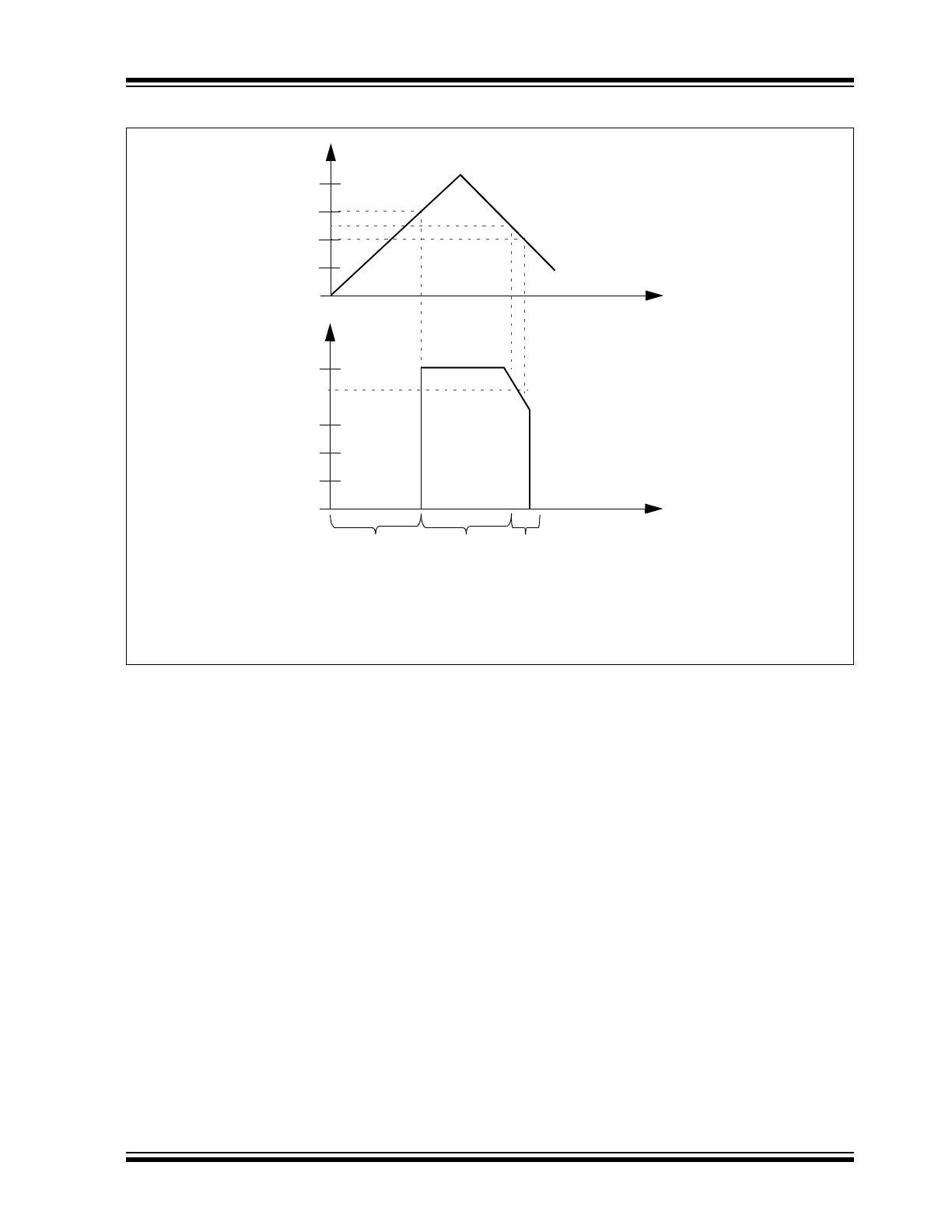
FIGURE 1-4:
VOLTAGE REGULATOR OUTPUT ON POWER-ON RESET
Note 1:
Start-up, V
BAT
< 6.0V, regulator off.
2:
V
BAT
> 6.0V, regulator on.
3:
V
BAT
≤
5.5V, regulator tracks V
BAT
, regulator will turn
off when V
REG
< 3.5V.
5.5
3.5
3
0
V
REG
V
---------------
(1)
(2)
(3)
t
0
t
6
2
8
4
V
BAT
V
--------------
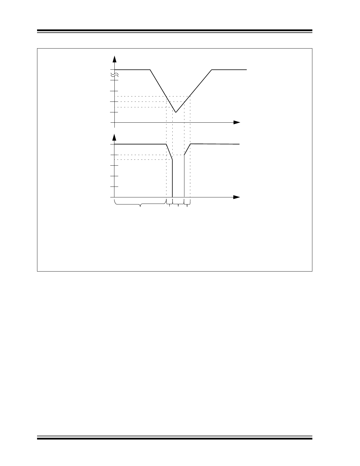
MCP201
DS21730F-page 10
©
2007 Microchip Technology Inc.
FIGURE 1-5:
VOLTAGE REGULATOR OUTPUT ON POWER DIP
Note 1:
Voltage regulator on.
2:
V
REG
≤
5.5V, regulator tracks V
BAT
until V
REG
< 3.5V.
3:
V
REG
< 3.5V, regulator is off. If the voltage regulator should shut
off due to V
REG
falling below 3.5V, the V
BAT
must rise to 6.0V to
turn V
REG
back on.
4:
V
REG
> 4.0V, voltage regulator tracks V
DD
, when V
REG
> 4.0V.
5
3.5
3
0
V
REG
V
---------------
(1)
(2) (3)
t
0
t
6
2
8
4
3.5
V
BAT
V
--------------
12
(4)
4