
2010-2016 Microchip Technology Inc.
DS20002230G-page 1
MCP2003/4/3A/4A
Features
• The MCP2003/2003A and MCP2004/2004A are
Compliant with Local Interconnect Network (LIN)
Bus Specifications 1.3, 2.0 and 2.1, and are
Compliant to SAE J2602
• Supports Baud Rates up to 20 Kbaud
with
LIN Bus Compatible Output Driver
• 43V Load Dump Protected
• Very Low/High Electromagnetic Immunity (EMI)
meets Stringent Original Equipment
Manufacturers (OEM) Requirements
• Very High Electrostatic Discharge (ESD)
Immunity:
- >20 kV on V
BB
(IEC 61000-4-2)
- >14 kV on L
BUS
(IEC 61000-4-2)
• Very High Immunity to RF Disturbances meets
Stringent OEM Requirements
• Wide Supply Voltage, 6.0V-27.0V Continuous
• Extended Temperature Range: -40°C to +125°C
• Interface to PIC
®
MCU EUSART and Standard
USARTs
• LIN Bus Pin:
- Internal pull-up resistor and diode
- Protected against battery shorts
- Protected against loss of ground
- High-current drive
• Automatic Thermal Shutdown
• Low-Power mode:
- Receiver monitoring bus and transmitter off
(
5 µA)
Description
This device provides a bidirectional, half-duplex commu-
nication, physical interface to automotive and industrial
LIN systems to meet the LIN Bus Specification
Revision 2.1 and SAE J2602. The device is short-circuit
and overtemperature protected by internal circuitry. The
device has been specifically designed to operate in the
automotive operating environment and will survive all
specified transient conditions, while meeting all of the
stringent quiescent current requirements.
MCP200X family members:
• 8-pin PDIP, DFN and SOIC packages:
- MCP2003: LIN bus compatible driver with
WAKE pins, wake-up on falling edge of L
BUS
- MCP2003A: LIN bus compatible driver with
WAKE pins, wake-up on rising edge of L
BUS
- MCP2004: LIN bus compatible driver with
FAULT/T
XE
pins, wake-up on falling edge of
L
BUS
- MCP2004A: LIN bus compatible driver with
FAULT/T
XE
pins, wake-up on rising edge of
L
BUS
Package Types
MCP2004/2004A
PDIP, SOIC
FAULT/T
XE
CS/WAKE
T
XD
V
BB
L
BUS
1
2
3
4
8
7
6
5 V
SS
V
REN
R
XD
MCP2003/2003A
PDIP, SOIC
WAKE
CS
T
XD
V
BB
L
BUS
1
2
3
4
8
7
6
5 V
SS
V
REN
R
XD
MCP2003/2003A
4x4 DFN
*
WAKE
CS
T
XD
V
BB
L
BUS
1
2
3
4
8
7
6
5 V
SS
V
REN
R
XD
EP
9
MCP2004/2004A
4x4 DFN
*
FAULT/T
XE
CS/WAKE
T
XD
V
BB
L
BUS
1
2
3
4
8
7
6
5 V
SS
V
REN
R
XD
EP
9
* Includes Exposed Thermal Pad (EP); see
Table 1-2
.
LIN J2602 Transceiver
Not Recommended for New Designs
Please use ATA663211 or MCP2003B
MCP2003/4/3A/4A
DS20002230G-page 2
2010-2016 Microchip Technology Inc.
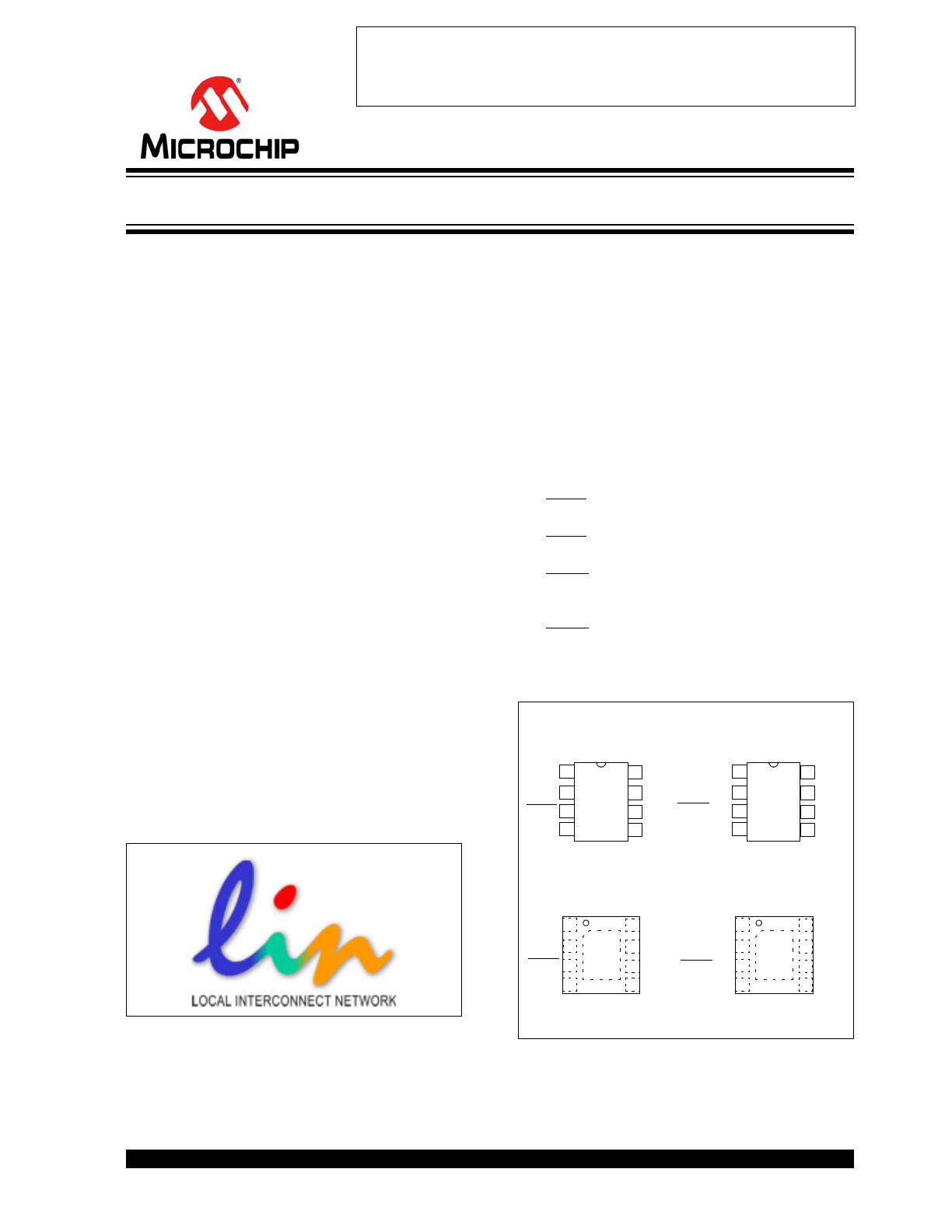
MCP2003/2003A Block Diagram
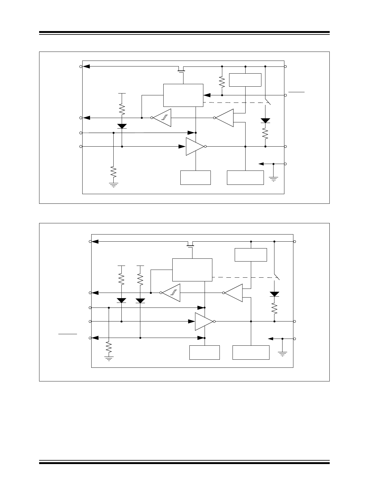
MCP2004/2004A Block Diagram
Thermal
Protection
V
REN
R
XD
T
XD
V
BB
L
BUS
V
SS
~30 k
CS
Wake-up
Logic and
Power Control
Short-Circuit
Protection
4.3V
WAKE
Ratiometric
Reference
–
+
OC
Thermal
Protection
V
REN
FAULT/T
XE
R
XD
T
XD
V
BB
L
BUS
V
SS
~30 k
CS/WAKE
Wake-up
Logic and
Power Control
Short-Circuit
Protection
4.3V
4.3V
–
+
Ratiometric
Reference
OC

2010-2016 Microchip Technology Inc.
DS20002230G-page 3
MCP2003/4/3A/4A
1.0
DEVICE OVERVIEW
The MCP2003/4/3A/4A devices provide a physical
interface between a microcontroller and a LIN bus.
These devices will translate the CMOS/TTL logic levels
to the LIN logic level and vice versa. It is intended for
automotive and industrial applications with serial bus
speeds up to 20 Kbaud.
LIN Bus Specification Revision 2.1 requires that the
transceiver of all nodes in the system is connected via
the LIN pin, referenced to ground, and with a maximum
external termination resistance load of 510
from LIN
bus to battery supply. The 510
corresponds to
1 master and 15 slave nodes.
The V
REN
pin can be used to drive the logic input of an
external voltage regulator. This pin is high in all modes
except for Power-Down mode.
1.1
External Protection
1.1.1
REVERSE BATTERY PROTECTION
An external reverse battery blocking diode should be
used to provide polarity protection (see
Example 1-1
).
1.1.2
TRANSIENT VOLTAGE
PROTECTION (LOAD DUMP)
An external 43V Transient Suppressor (TVS) diode,
between V
BB
and ground with a 50
Transient
Protection Resistor (R
TP
) in series with the battery
supply and the V
BB
pin, serve to protect the device from
power transients (see
Example 1-1
) and ESD events.
While this protection is optional, it is considered good
engineering practice.
1.2
Internal Protection
1.2.1
ESD PROTECTION
For component-level ESD ratings, please refer to the
maximum operation specifications.
1.2.2
GROUND LOSS PROTECTION
The LIN Bus Specification states that the LIN pin must
transition to the Recessive state when the ground is
disconnected. Therefore, a loss of ground effectively
forces the LIN line to a high-impedance level.
1.2.3
THERMAL PROTECTION
The thermal protection circuit monitors the die
temperature and is able to shut down the
LIN
transmitter.
There are two causes for a thermal overload. A thermal
shutdown can be triggered by either, or both, of the
following thermal overload conditions:
• LIN bus output overload
• Increase in die temperature due to increase in
environment temperature
Driving the T
XD
pin and checking the R
XD
pin makes it
possible to determine whether there is a bus contention
(R
XD
= low, T
XD
= high) or a thermal overload condition
(R
XD
= high, T
XD
= low). After a thermal overload event,
the device will automatically recover once the die
temperature has fallen below the recovery temperature
threshold (see
Figure 1-1
).
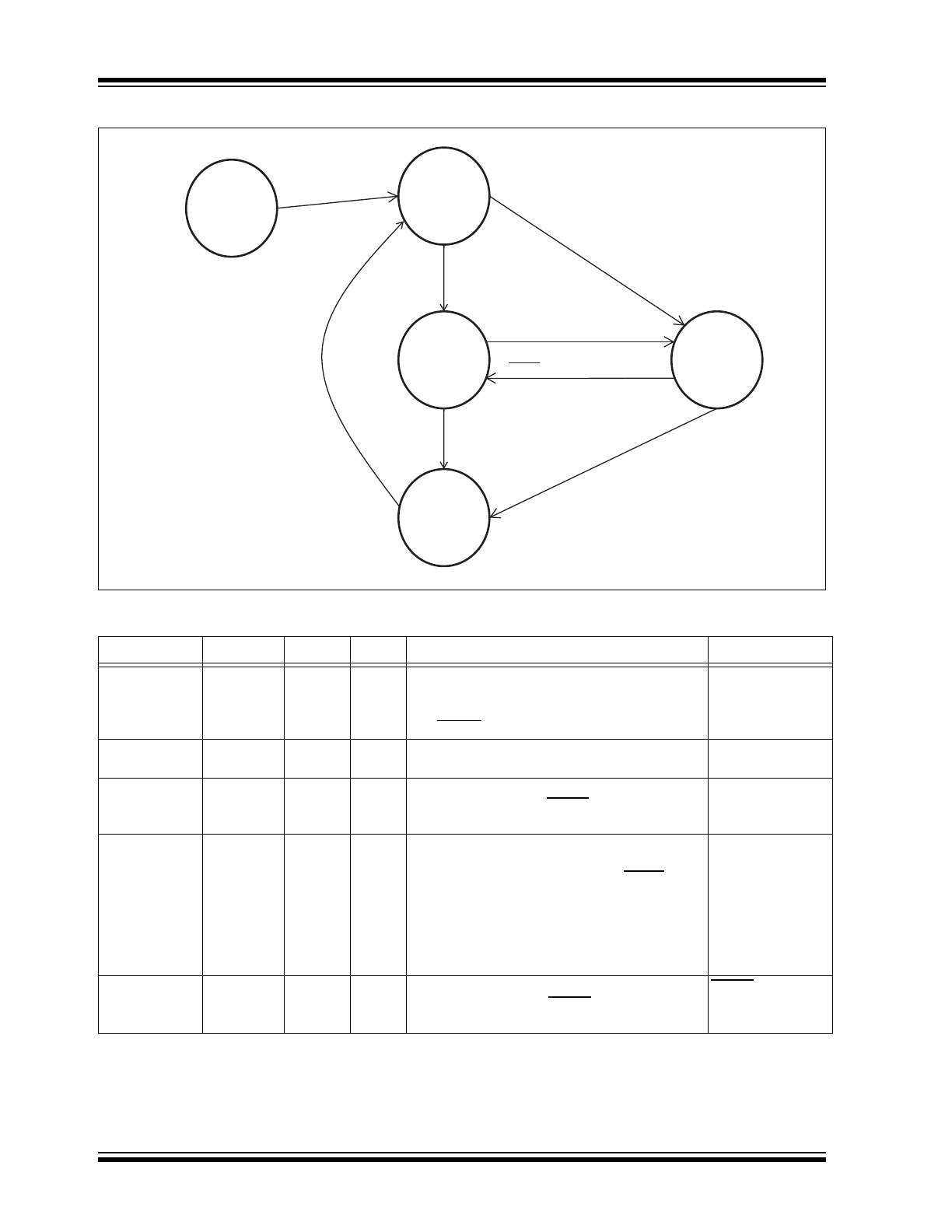
FIGURE 1-1:
THERMAL SHUTDOWN
STATE DIAGRAM
Operation
Mode
Transmitter
Shutdown
Shorted LIN Bus
to V
BB
Temp < Shutdown
TEMP
MCP2003/4/3A/4A
DS20002230G-page 4
2010-2016 Microchip Technology Inc.
1.3
Modes of Operation
For an overview of all operational modes, refer to
Table 1-1
.
1.3.1
POWER-DOWN MODE
In Power-Down mode, everything is off except the
wake-up section. This is the lowest power mode. The
receiver is off, thus its output is open-drain.
On CS going to a high level or a falling edge on WAKE
(MCP2003/MCP2003A only), the device will enter
Ready mode as soon as the internal voltage stabilizes.
Refer to
Section 2.4 “AC Specifications”
for further
information. In addition, LIN bus activity will change the
device from Power-Down mode to Ready mode;
MCP2003/4 wakes up on a falling edge on
L
BUS
,
followed by a low level lasting at least 20 µs.
MCP2003A/4A wakes up on a rising edge on
L
BUS
,
followed by a high level lasting 70 µs, typically.
See
Figures 1-2
to
1-5
about remote wake-up. If CS is held
high as the device transitions from Power-Down to
Ready mode, the device will transition to either Opera-
tion or Transmitter Off mode, depending on the T
XD
input, as soon as internal voltages stabilize.
1.3.2
READY MODE
Upon entering Ready mode, V
REN
is enabled and the
receiver detect circuit is powered up. The transmitter
remains disabled and the device is ready to receive
data but not to transmit.
Upon V
BB
supply pin power-on, the device will remain
in Ready mode as long as CS is low. When CS
transitions high, the device will either enter Operation
mode, if the T
XD
pin is held high, or the device will enter
Transmitter Off mode, if the T
XD
pin is held low.
1.3.3
OPERATION MODE
In this mode, all internal modules are operational.
The device will go into Power-Down mode on the falling
edge of CS. For the MCP2003/4 device, a specific
process should be followed to put all nodes into Power-
Down mode. Refer to
Section 1.6 “MCP2003/4 and
MCP2003A/4A Difference Details”
and
Figure 1-6
.
The device will enter Transmitter Off mode in the event
of a Fault condition, such as thermal overload, bus
contention and T
XD
timer expiration.
The MCP2004/2004A device can also enter Transmitter
Off mode if the FAULT/T
XE
pin is pulled low. The V
BB
to
L
BUS
pull-up resistor is connected only in Operation
mode.
1.3.4
TRANSMITTER OFF MODE
Transmitter Off mode is reached whenever the
transmitter is disabled, either due to a Fault condition or
pulling the FAULT/T
XE
pin low on the MCP2004/2004A.
The Fault conditions include: thermal overload, bus
contention, R
XD
monitoring or T
XD
timer expiration.
The device will go into Power-Down mode on the falling
edge of CS or return to Operation mode if all Faults are
resolved and the FAULT/T
XE
pin on the MCP2004/2004A
is high.
FIGURE 1-2:
OPERATIONAL MODES STATE DIAGRAM – MCP2003
POR
V
REN
OFF
RX OFF
TX OFF
V
BAT
> 5.5V
Ready
V
REN
ON
RX ON
TX OFF
T
OFF
Mode
V
REN
ON
RX ON
TX OFF
Operation
Mode
V
REN
ON
RX ON
TX ON
POWER-
DOWN
V
REN
OFF
RX OFF
TX OFF
CS =
1 and T
XD
=
0
CS =
1 and T
XD
=
1
CS =
1 and T
XD
=
1 and No Fault
Fault (thermal or timer)
CS =
0
Falling Edge on LIN
or CS =
1
or Falling Edge on WAKE Pin
CS =
0
2010-2016 Microchip Technology Inc.
DS20002230G-page 5
MCP2003/4/3A/4A
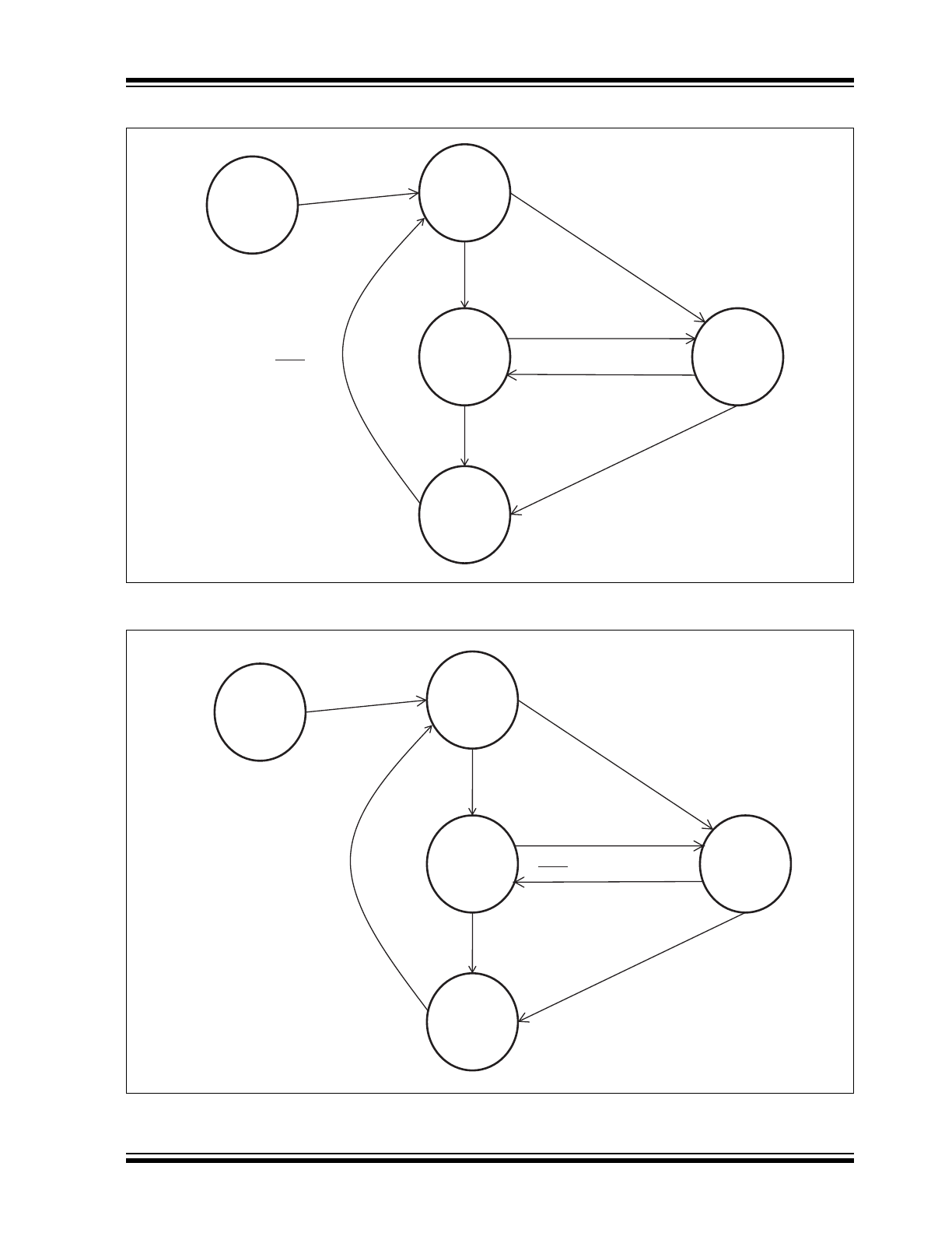
FIGURE 1-3:
OPERATIONAL MODES STATE DIAGRAM – MCP2003A
FIGURE 1-4:
OPERATIONAL MODES STATE DIAGRAM – MCP2004
POR
V
REN
OFF
RX OFF
TX OFF
V
BAT
> 5.5V
Ready
V
REN
ON
RX OFF
TX OFF
T
OFF
Mode
V
REN
ON
RX ON
TX OFF
Operation
Mode
V
REN
ON
RX ON
TX ON
POWER-
DOWN
V
REN
OFF
RX OFF
TX OFF
CS =
1 and T
XD
=
0
CS =
1 and T
XD
=
1
CS =
1 and T
XD
=
1 and No Fault
Fault (thermal or timer)
CS =
0
Rising Edge on LIN
or CS =
1
or Falling Edge on WAKE Pin
CS =
0
POR
V
REN
OFF
RX OFF
TX OFF
V
BAT
> 5.5V
Ready
V
REN
ON
RX ON
TX OFF
T
OFF
Mode
V
REN
ON
RX ON
TX OFF
Operation
Mode
V
REN
ON
RX ON
TX ON
POWER-
DOWN
V
REN
OFF
RX OFF
TX OFF
CS =
1 and (T
XE
=
0 or T
XD
=
0)
CS =
1 and T
XD
=
1 and T
XE
=
1
CS =
1 and T
XD
=
1 and T
XE
=
1
and No Fault
CS =
0
Falling Edge on LIN or
CS =
1
CS =
0
Fault (thermal or time-out) or
FAULT/T
XE
=
0
MCP2003/4/3A/4A
DS20002230G-page 6
2010-2016 Microchip Technology Inc.
FIGURE 1-5:
OPERATIONAL MODES STATE DIAGRAM – MCP2004A
TABLE 1-1:
OVERVIEW OF OPERATIONAL MODES
State
Transmitter Receiver
V
REN
Operation
Comments
POR
OFF
OFF
OFF
Check CS; if low, then proceed to Ready mode.
If high, transitions to either T
OFF
or Operation
mode, depending on T
XD
(MCP2003/A), or T
XD
and FAULT/T
XE
(MCP2004/A).
V
BB
> V
BB(MIN)
and
internal supply is
stable
Ready
OFF
ON
ON
If CS is a high level, then proceed to Operation
or T
OFF
mode.
Bus Off state
Operation
ON
ON
ON
If CS is a low level, then proceed to
Power-Down mode. If FAULT/T
XE
is a low level,
then proceed to Transmitter Off mode.
Normal Operation
mode
Power-Down
OFF
Activity
Detect
OFF
On CS high level, proceed to Ready mode; then
proceed to either Operation mode or T
OFF
mode.
MCP2003/2003A: Falling edge on WAKE will
put the device into Ready mode.
MCP2003/MCP2004: Falling edge on LIN bus
will put the device into Ready mode.
MCP2003A/MCP2004A: Rising edge on
LIN bus will put the device into Ready mode.
Low-Power mode
Transmitter Off
OFF
ON
ON
If CS is a low level, then proceed to
Power-Down mode. If FAULT/T
XE
and T
XD
are
high, then proceed to Operation mode.
FAULT/T
XE
is only
available on
MCP2004/2004A
POR
V
REN
OFF
RX OFF
TX OFF
V
BAT
> 5.5V
Ready
V
REN
ON
RX ON
TX OFF
T
OFF
Mode
V
REN
ON
RX ON
TX OFF
Operation
Mode
V
REN
ON
RX ON
TX ON
POWER-
DOWN
V
REN
OFF
RX OFF
TX OFF
CS =
1 and (T
XE
=
0 or T
XD
=
0)
CS =
1 and T
XD
=
1 and T
XE
=
1
CS =
1 and T
XD
=
1 and
T
XE
=
1 and No Fault
Fault (thermal or time-out) or
FAULT/T
XE
=
0
CS =
0
Rising Edge on LIN
or CS =
1
CS =
0
2010-2016 Microchip Technology Inc.
DS20002230G-page 7
MCP2003/4/3A/4A
1.4
Typical Applications
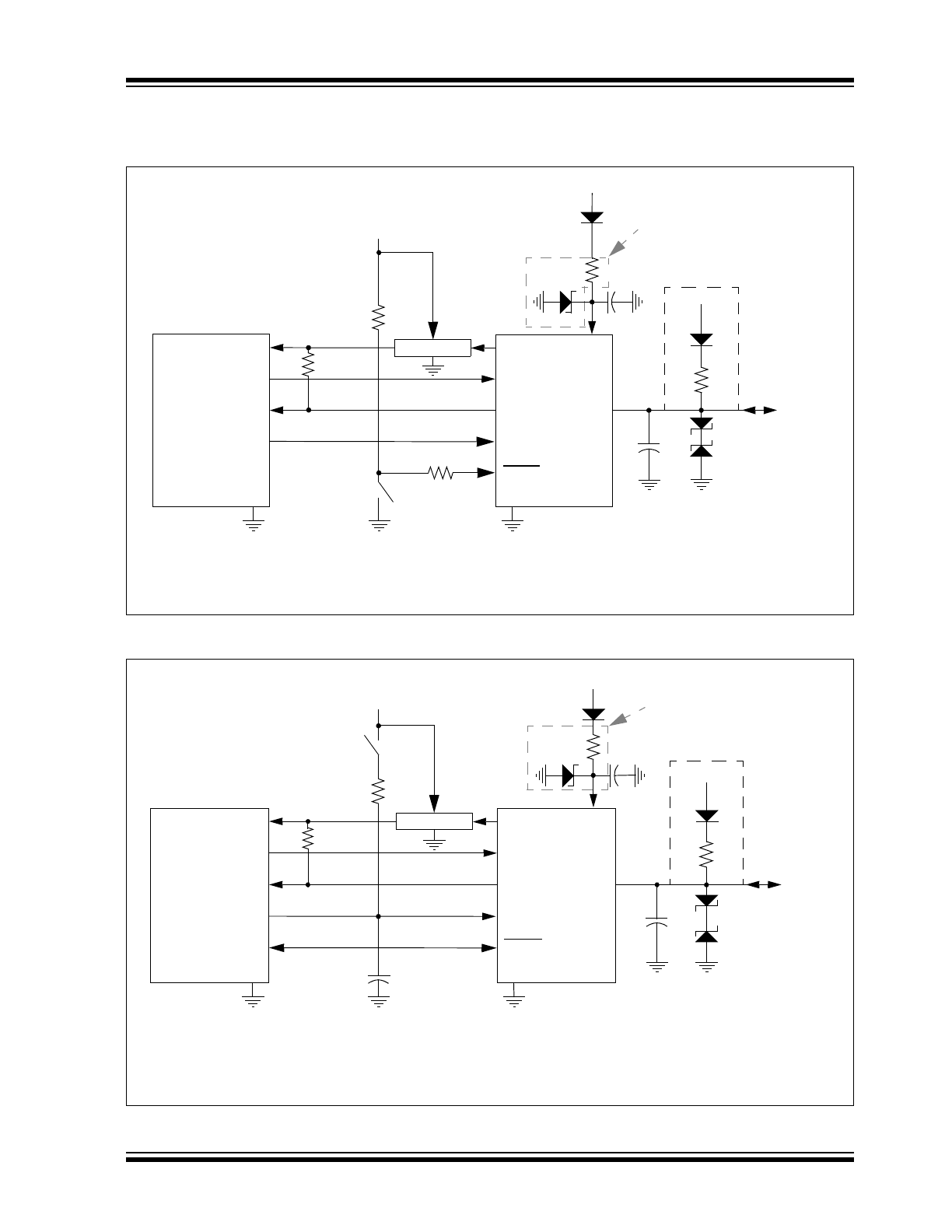
EXAMPLE 1-1:
TYPICAL MCP2003/2003A APPLICATION
EXAMPLE 1-2:
TYPICAL MCP2004/2004A APPLICATION
LIN Bus
V
DD
T
XD
R
XD
+12
1.0 µF
I/O
50
43V
1 k
+12
Master Node Only
+12
3.9 k
Wake-up
Voltage Reg
(Note 1)
Note 1:
For applications with current requirements of less than 20 mA, the connection to +12V can be deleted and voltage
to the regulator can be supplied directly from the V
REN
pin.
2:
ESD protection diode.
4.7 k
Optional Resistor and
33 k
MMBZ27V
(2)
220 pF
V
BB
L
BUS
V
REN
T
XD
R
XD
V
SS
CS
WAKE
Transient Suppressor
LIN Bus
V
DD
T
XD
R
XD
1.0 µF
I/O
I/O
50
43V
1 k
+12
Master Node Only
+12
220 k
Wake-up
Voltage Reg
100 nF
4.7 k
+12
Optional Resistor and
MMBZ27V
(2)
220 pF
(Note 1)
V
BB
L
BUS
V
REN
T
XD
R
XD
V
SS
CS/WAKE
FAULT/T
XE
Transient Suppressor
Note 1:
For applications with current requirements of less than 20 mA, the connection to +12V can be deleted and voltage
to the regulator can be supplied directly from the V
REN
pin.
2:
ESD protection diode.
MCP2003/4/3A/4A
DS20002230G-page 8
2010-2016 Microchip Technology Inc.
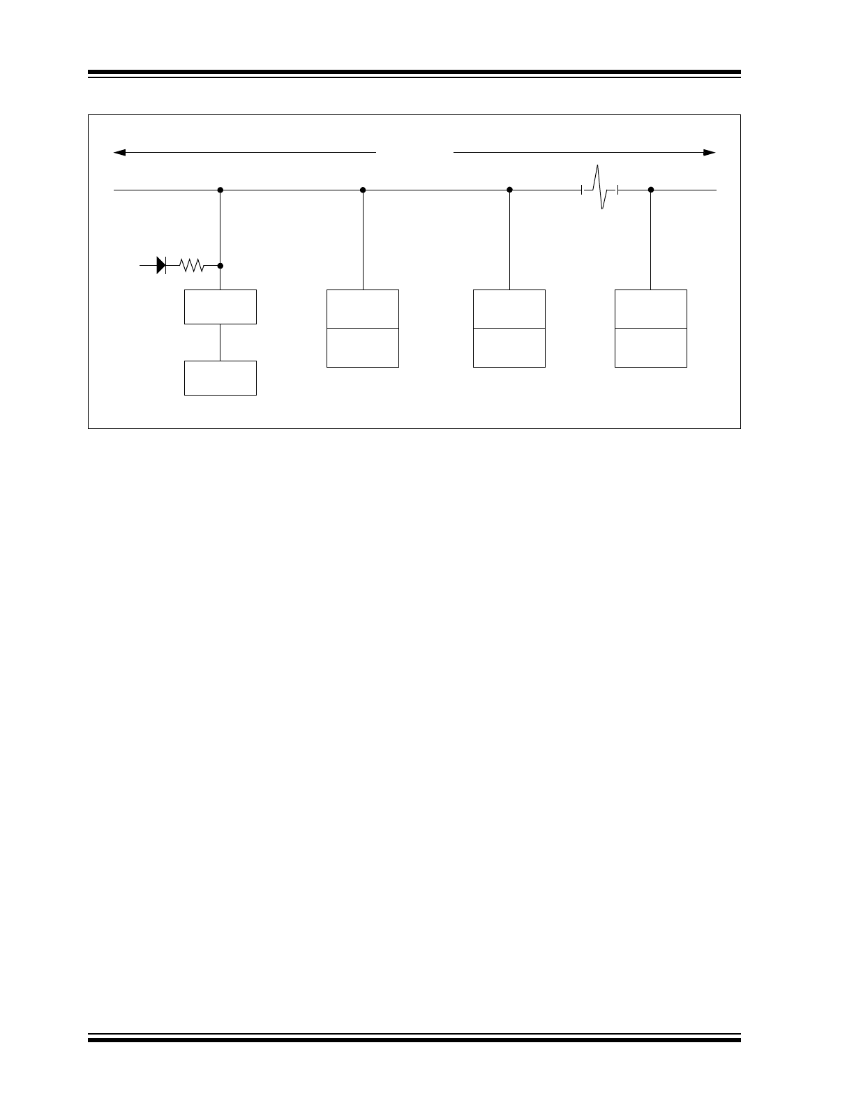
EXAMPLE 1-3:
TYPICAL LIN NETWORK CONFIGURATION
Master
(MCU)
1 k
V
BB
Slave 1
(MCU)
40m + Return
LIN Bus
LIN Bus
MCP2000X
LIN Bus
MCP200X
LIN Bus
MCP200X
Slave 2
(MCU)
LIN Bus
MCP200X
Slave n < 23
(MCU)
2010-2016 Microchip Technology Inc.
DS20002230G-page 9
MCP2003/4/3A/4A
1.5
Pin Descriptions
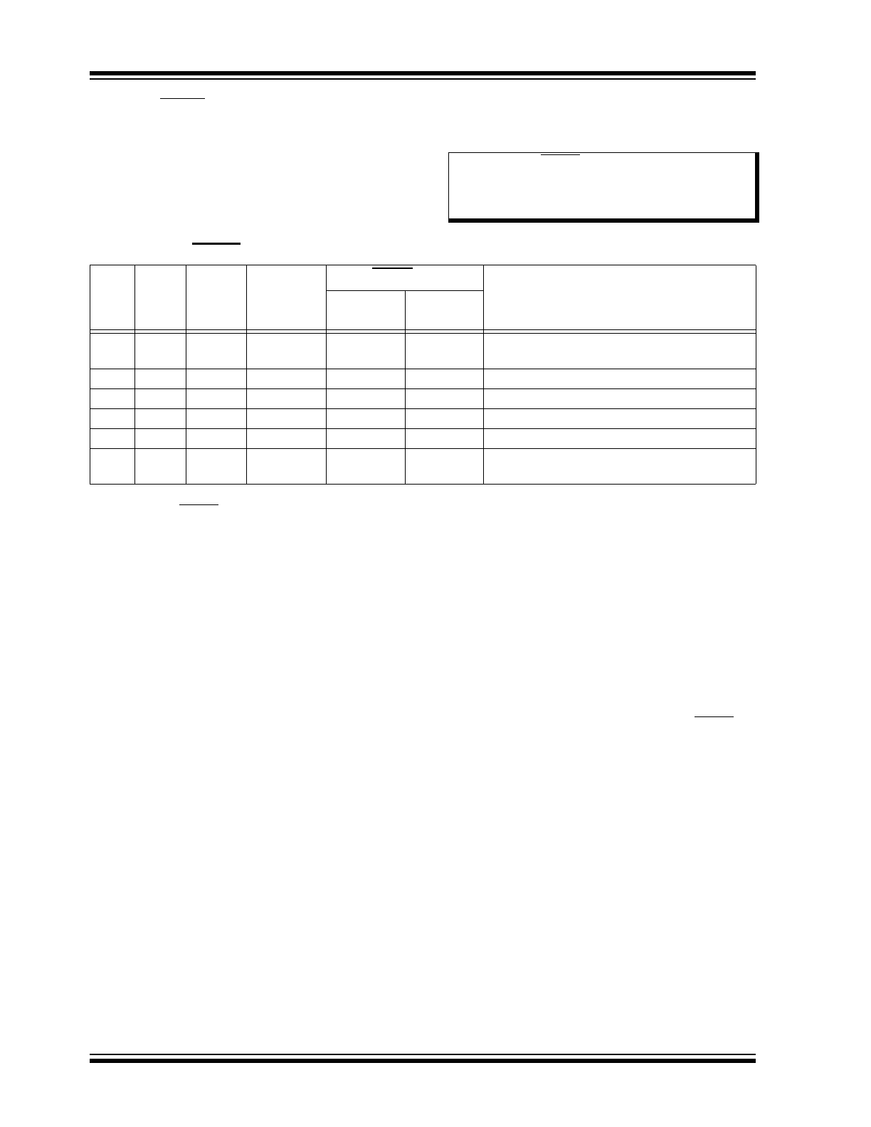
TABLE 1-2:
PINOUT DESCRIPTIONS
1.5.1
RECEIVE DATA OUTPUT (R
XD
)
The Receive Data Output pin is an Open-Drain (OD)
output and follows the state of the LIN pin, except in
Power-Down mode.
1.5.1.1
R
XD
Monitoring
The
R
XD
pin is internally monitored. It has to be at a
high level (> 2.5V typical) while
L
BUS
is recessive.
Otherwise, an internal Fault will be created and the
device will transition to Transmitter Off mode. On the
MCP2004/2004A, the FAULT/
T
XE
pin will be driven low
to indicate the Transmitter Off state.
1.5.2
CHIP SELECT (CS)
This is the Chip Select input pin. An internal pull-down
resistor will keep the CS pin low. This is done to ensure
that no disruptive data will be present on the bus while
the microcontroller is executing a Power-on Reset and
an I/O initialization sequence. The pin must detect a high
level to activate the transmitter. An internal low-pass
filter, with a typical time constant of 10 µs, prevents
unwanted wake-up (or transition to Power-Down mode)
on glitches.
If CS = 0 when the V
BB
supply is turned on, the device
goes to Ready mode as soon as internal voltages sta-
bilize and stays there as long as the CS pin is held low
(0). In Ready mode, the receiver is on and the LIN
transmitter driver is off.
If CS = 1 when the V
BB
supply is turned on, the device
will proceed to Operation mode or T
OFF
mode (refer to
Figures 1-2
to
1-5
) as soon as internal voltages
stabilize.
This pin may also be used as a local wake-up input
(refer to
Example 1-1
). In this implementation, the
microcontroller I/O controlling the CS should be con-
verted to a high-impedance input, allowing the internal
pull-down resistor to keep CS low. An external switch,
or other source, can then wake-up both the transceiver
and the microcontroller (if powered). Refer to
Section 1.3 “Modes of Operation”
, for detailed
operation of CS.
1.5.3
WAKE-UP INPUT (WAKE)
This pin is only available on the MCP2003/2003A.
The WAKE pin has an internal 800 kΩ pull-up to V
BB
.
A falling edge on the WAKE pin causes the device to
wake from Power-Down mode. Upon waking, the
MCP2003/3A will enter Ready mode.
Pin Name
8-Lead
PDIP,
SOIC
4x4
DFN
MCP2003/2003A
MCP2004/2004A
Normal Operation
Normal Operation
R
XD
1
1
Receive Data Output (OD),
HV tolerant
Receive Data Output (OD),
HV tolerant
CS
2
2
Chip Select (TTL), HV tolerant
Chip Select/Local WAKE (TTL),
HV tolerant
WAKE
(MCP2003/2003A only)
3
3
Wake-up, HV tolerant
Fault Detect Output (OD),
Transmitter Enable (TTL),
HV tolerant
FAULT/T
XE
(MCP2004/2004A only)
T
XD
4
4
Transmit Data Input (TTL),
HV tolerant
Transmit Data Input (TTL),
HV tolerant
V
SS
5
5
Ground
Ground
L
BUS
6
6
LIN Bus (bidirectional)
LIN Bus (bidirectional)
V
BB
7
7
Battery Positive
Battery Positive
V
REN
8
8
Voltage Regulator Enable Output Voltage Regulator Enable Output
EP
—
9
Exposed Thermal Pad; do not
electrically connect or connect
to V
SS
Exposed Thermal Pad; do not
electrically connect or connect
to V
SS
Legend:
TTL = TTL Input Buffer; OD = Open-Drain Output
Note:
It is not recommended to tie CS high as
this can result in the device entering
Operation mode before the microcontrol-
ler is initialized and may result in
unintentional LIN traffic.
MCP2003/4/3A/4A
DS20002230G-page 10
2010-2016 Microchip Technology Inc.
1.5.4
FAULT/T
XE
This pin is only available on the MCP2004/2004A. This
pin is bidirectional and allows disabling of the transmitter,
as well as Fault reporting related to disabling the
transmitter. This pin is an open-drain output with states
as defined in
Table 1-3
. The transmitter is disabled
whenever this pin is low (‘0’), either from an internal
Fault condition or by an external drive. While the trans-
mitter is disabled, the internal 30 k
pull-up resistor on
the L
BUS
pin is also disconnected to reduce current.
TABLE 1-3:
FAULT/T
XE
TRUTH TABLE
1.5.5
TRANSMIT DATA INPUT (T
XD
)
The Transmit Data input pin has an internal pull-up.
The LIN pin is low (dominant) when T
XD
is low and high
(recessive) when T
XD
is high.
For extra bus security, T
XD
is internally forced to ‘1’
whenever the transmitter is disabled, regardless of the
external T
XD
voltage.
1.5.5.1
T
XD
Dominant Time-out
If T
XD
is driven low for longer than approximately
25 ms, the L
BUS
pin is switched to Recessive mode and
the part enters T
OFF
mode. This is to prevent the LIN
node from permanently driving the LIN bus dominant.
The transmitter is reenabled on the T
XD
rising edge.
1.5.6
GROUND (V
SS
)
This is the Ground pin.
1.5.7
LIN BUS (L
BUS
)
The bidirectional LIN Bus pin (L
BUS
) is controlled by the
T
XD
input. L
BUS
has a current-limited open-collector
output. To reduce EMI, the edges, during the signal
changes, are slope controlled, and include corner
rounding control for both falling and rising edges.
The internal LIN receiver observes the activities on the
LIN bus and matches the output signal, R
XD
, to follow
the state of the L
BUS
pin.
1.5.7.1
Bus Dominant Timer
The Bus Dominant Timer is an internal timer that
deactivates the L
BUS
transmitter after approximately
25 ms of Dominant state on the L
BUS
pin. The timer is
reset on any recessive L
BUS
state.
The LIN bus transmitter will be reenabled after a
Recessive state on the L
BUS
pin as long as CS is high.
Disabling can be caused by the LIN bus being
externally held dominant or by T
XD
being driven low.
Additionally, on the MCP2004/2004A, the FAULT pin
will be driven low to indicate the Transmitter Off state.
1.5.8
BATTERY (V
BB
)
This is the Battery Positive Supply Voltage pin.
1.5.9
VOLTAGE REGULATOR ENABLE
OUTPUT (V
REN
)
This is the External Voltage Regulator Enable pin. The
open source output is pulled high to V
BB
in all modes,
except Power-Down.
1.5.10
EXPOSED THERMAL PAD (EP)
Do not electrically connect or connect to V
SS
.
Note:
The FAULT/T
XE
pin is true (‘0’) whenever
the internal circuits have detected a short
or thermal excursion and have disabled
the L
BUS
output driver.
T
XD
In
R
XD
Out
LIN
BUS
I/O
Thermal
Override
FAULT/T
XE
Definition
External
Input
Driven
Output
L
H
V
BB
OFF
H
L
FAULT
, T
XD
driven low, L
BUS
shorted to V
BB
(
Note 1
)
H
H
V
BB
OFF
H
H
OK
L
L
GND
OFF
H
H
OK
H
L
GND
OFF
H
H
OK
, data is being received from L
BUS
x
x
V
BB
ON
H
L
FAULT
, transceiver in thermal shutdown
x
x
V
BB
x
L
x
NO FAULT
, the CPU is commanding the
transceiver to turn off the transmitter driver
Legend:
x = don’t care.
Note 1:
The FAULT/T
XE
is valid after approximately 25 µs after the T
XD
falling edge. This is to eliminate false Fault
reporting during bus propagation delays.