
2012-2013 Microchip Technology Inc.
DS22326B-page 1
MCP19035
Features:
• Input Voltage Range: from 4.5V to 30V
• Targeted for Low-Voltage Power Trains with
Output Current up to 20A
• High-Speed Voltage Mode, Analog Pulse-Width
Modulation Control
• Power Good Output
• Internal Oscillator, Reference Voltage and
Overcurrent Limit Threshold for Stand-Alone
Applications.
• Multiple Switching Frequency Options (F
SW
):
- 300 kHz
- 600 kHz
• Integrated Synchronous MOSFET Drivers
• Multiple Dead-Time Options
• Internal Blocking Device for Bootstrap Circuit
• Integrated Current Sense Capability for Short
Circuit Protection
• Internal Overtemperature Protection
• Under Voltage Lockout (UVLO)
• Integrated Linear Voltage Regulator
• 10-LD 3 X 3 mm DFN Package
Applications:
• Point of Loads
• Set-Top Boxes
• DSL Cable Modems
• FPGA’s/DSP’s Power Supply
• PC’s Graphic/Audio Cards
General Description
The MCP19035 is an application-optimized, high-
speed synchronous buck controller that operates from
input voltage sources up to 30V. This controller
implements a voltage-mode control architecture with a
fixed switching frequency of 300 kHz or 600 kHz. The
high-switching frequency facilitates the use of smaller
passive components, including the inductor and
input/output capacitors, allowing a compact, high-
performance power supply solution. The MCP19035
implements an adaptive anti-cross conduction scheme
to prevent shoot-through in the external power
MOSFETs. Furthermore, the MCP19035 offers multiple
dead-time options, enabling an additional degree of
optimization, allowing a higher efficiency power supply
design.
The MCP19035 controller is intended to be used for
applications providing up to 20A of output currents
across a wide input voltage range, up to 30V.
The SHDN input is used to turn the device on and off.
While turned off, the current consumption is minimized.
The MCP19035 offers a Power Good feature
(PWRGD), enabling fault detection and simplifying
sequencing.
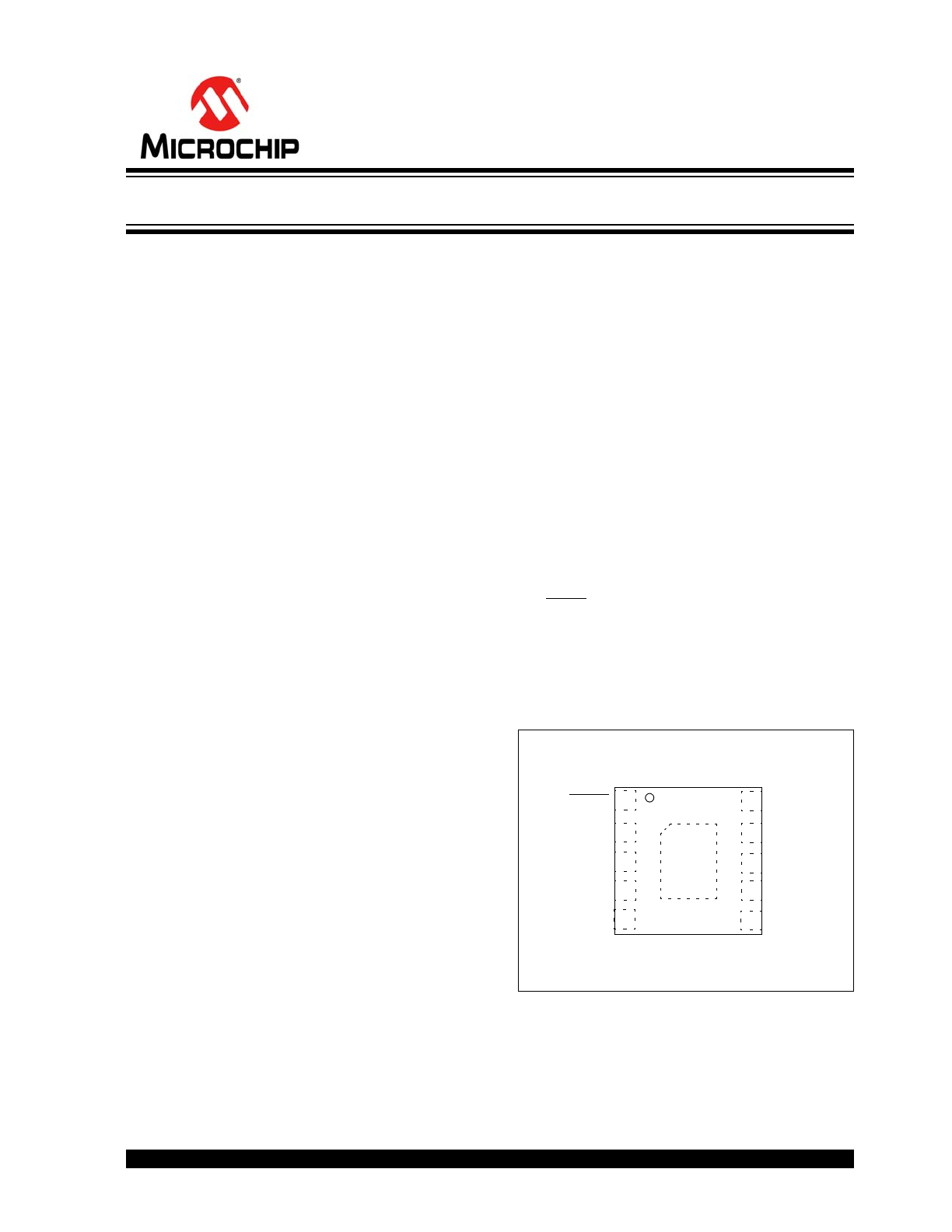
Package Types
MCP19035
3x3 DFN*
COMP
FB
V
IN
PHASE
BOOT
1
2
3
4
10
9
8
7 LDRV
HDRV
SHDN
* Includes Exposed Thermal Pad (EP); see
Table 3-1
.
EP
11
6
PWRGD
+V
CC
5
High-Speed Synchronous Buck Controller
MCP19035
DS22326B-page 2
2012-2013 Microchip Technology Inc.
Typical Application
C
IN
C
OUT
L
Q
1
Q
2
MCP19035
HDRV
LDRV
PHASE
BOOT
+V
CC
C
BOOT
C
VCC
+V
OUT
V
IN
PWRGD
COMP
FB
R
1
R
3
C
1
R
2
C
3
R
4
C
2
ON
OFF
SHDN
GND
+ V
IN
2012-2013 Microchip Technology Inc.
DS22326B-page 3
MCP19035
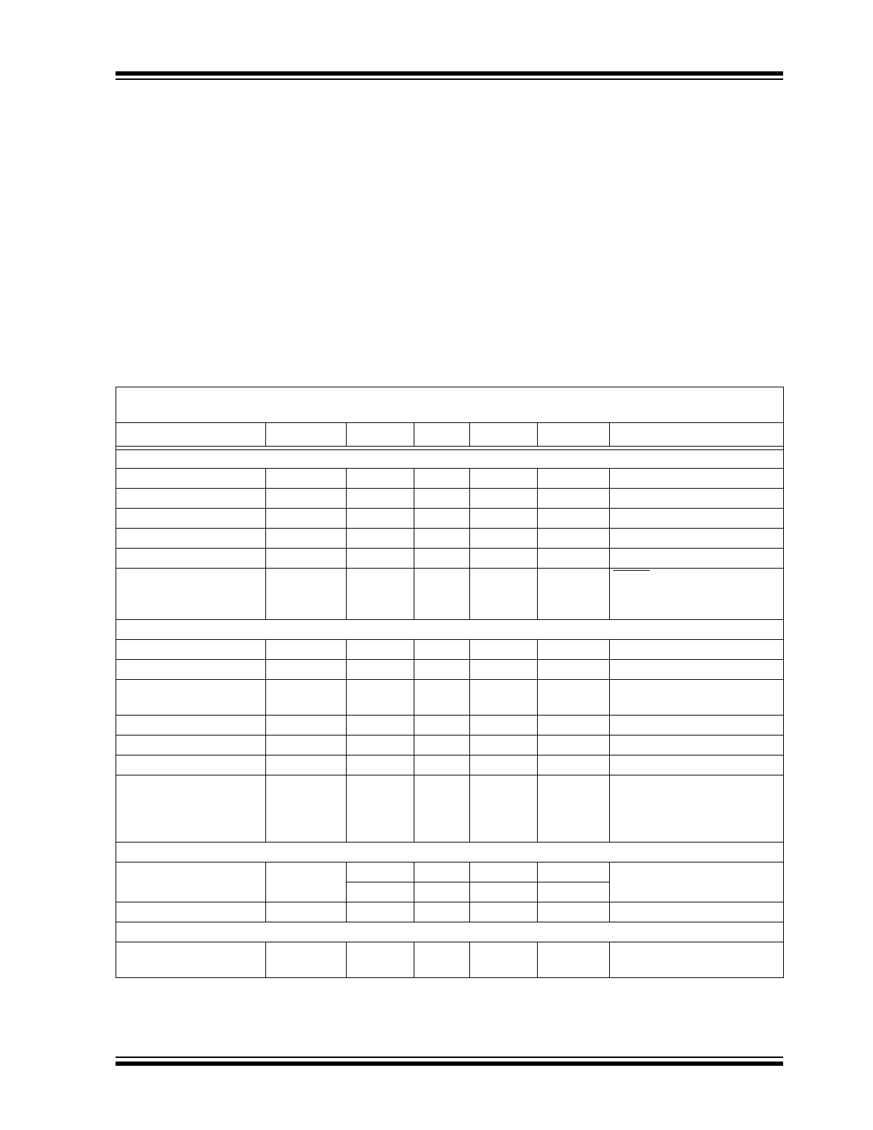
1.0
ELECTRICAL
CHARACTERISTICS
Absolute Maximum Ratings †
V
IN
- V
GND
........................................................ -0.3V to +32V
V
BOOT
................................................................ -0.3V to +37V
VHDRV, HDRV Pin................. +V
PHASE
-0.3V to V
BOOT
+0.3V
VLDRV, LDRV Pin.....................+ (V
GND
-0.3V) to (V
CC
+0.3V)
Max. Voltage on Any Pin ...........+ (V
GND
-0.3V) to (V
CC
+0.3V)
Storage Temperature ....................................-65°C to +150°C
Maximum Junction Temperature................................. +150°C
ESD protection on all pins (HBM) .................................... 2 kV
ESD protection on all pins (MM) .....................................200V
† Notice:
Stresses above those listed under “Maximum
Ratings” may cause permanent damage to the device.
This is a stress rating only and functional operation of
the device at those or any other conditions above those
indicated in the operational sections of this
specification is not intended. Exposure to maximum
rating conditions for extended periods may affect
device reliability.
DC ELECTRICAL CHARACTERISTICS
Electrical Specifications
: Unless otherwise noted, V
IN
= 12V, F
SW
= 300 kHz, C
IN
= 1.0 µF, T
A
= +25°C (for typical
values), T
A
= -40°C to +125°C (for minimum and maximum).
Parameters
Symbol
Min
Typ
Max
Units
Conditions
Inputs
Input Voltage Range
V
IN
4.5
—
30
V
UVLO (V
IN
Rising)
UVLO
ON
4
4.2
4.4
V
UVLO (V
IN
Falling)
UVLO
OFF
3.4
3.6
3.8
V
UVLO Hysteresis
UVLO
HYST
—
600
—
mV
Input Quiescent Current
I(V
IN
)
—
6
8
mA
Shutdown Current
I
IN_SHDN
—
25
50
µA
SHDN = GND.
Internal Voltage Regulator is
also disabled
Linear Regulator
Output Voltage
V
CC
4.875
5
5.125
V
6V
V
IN
< 30V
Output Current
I
VCC-OUT
50
—
mA
6.5V
V
IN
< 30V,
Note 2
Short-Circuit
Output Current
I
VCC-OUT_SC
—
—
100
mA
V
IN
= 6V, R
LOAD
< 0.1
Load Regulation
—
0.1
—
%
Note 1
Line Regulation
—
0.05
—
%
Note 1
Dropout Voltage
—
0.75
1.3
V
I
VCC_OUT
= 50 mA
Power Supply
Rejection Ratio
PSRR
—
70
—
dB
f
1000 Hz,
I
VCC_OUT
= 50 mA
C
IN
= 0 µF,
C
VCC-OUT
= 4.7 µF,
Note 1
Internal Oscillator
Switching Frequency
F
SW
255
300
345
kHz
2 options, see
Section 4.4,
Internal Oscillator
510
600
690
kHz
Ramp Signal Amplitude
V
RAMP
0.9
1
1.1
V
PP
Note 1
Reference Voltage
Reference Voltage
Generator
V
REF
585
600
615
mV
Note 1:
Ensured by design. Not production tested.
2:
Limited by the maximum power dissipation of the case.
3:
Possibility to be adjusted for high volumes.
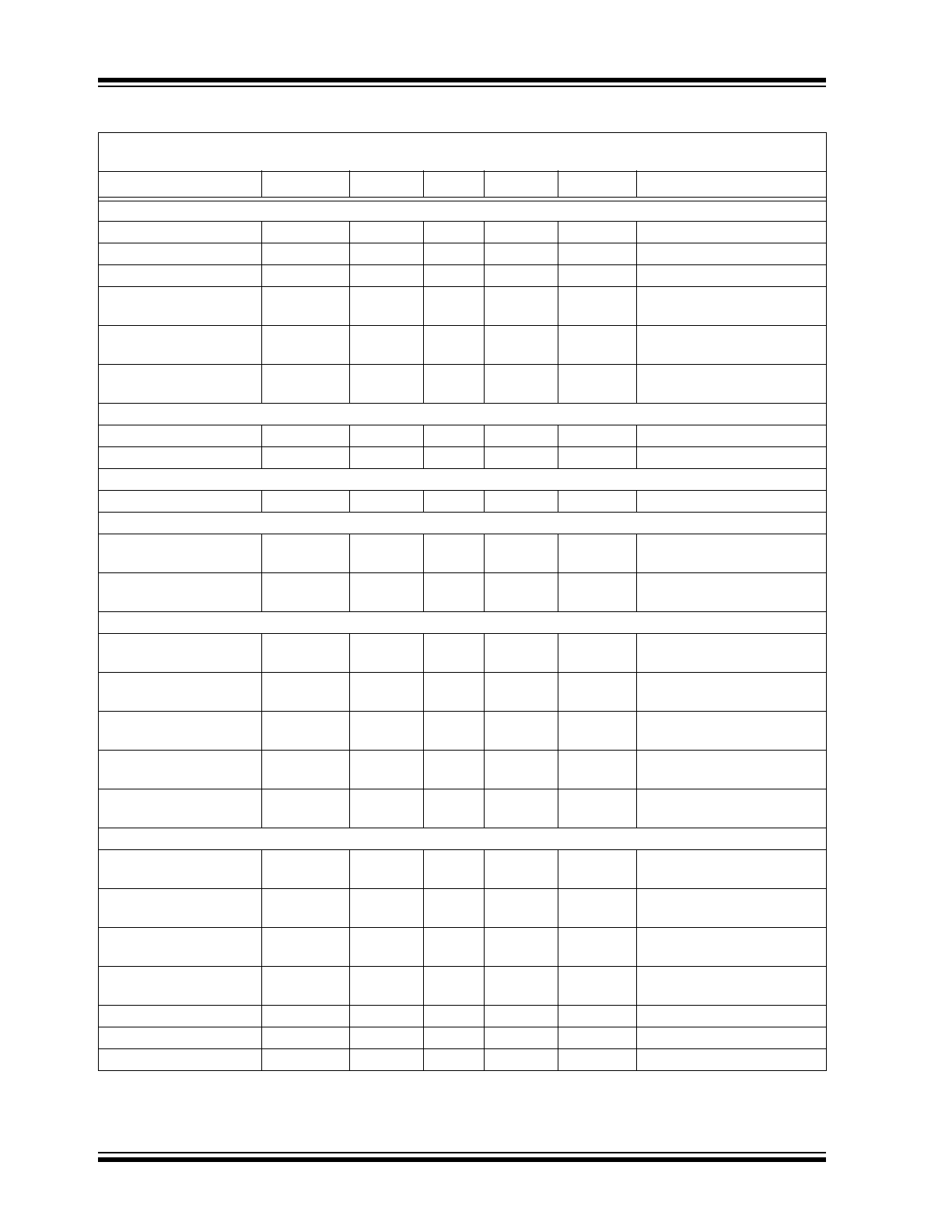
MCP19035
DS22326B-page 4
2012-2013 Microchip Technology Inc.
Error Amplifier
Gain Bandwidth Product
GBP
6.5
10
—
MHz
Note 1
Open Loop Gain
A
OL
70
80
—
dB
Note 1
Input Offset Voltage
V
OS
-5
0.1
5
mV
Note 1
Input Bias Current
(FB Pin)
I
BIAS
—
—
5
nA
Note 1
Error Amplifier
Sink Current
I
SINK
—
5
—
mA
Note 1
Error Amplifier
Source Current
I
SOURCE
—
5
—
mA
Note 1
PWM Section
Maximum Duty Cycle
DC
MAX
85
—
—
%
Note 1
Minimum ON time
t
ON(MIN)
50
—
100
ns
6V
V
IN
< 30V,
Note 1
Soft Start
Soft Start Time
t
SS
—
8
—
ms
Shutdown
Logic Low-to-High
Threshold
SHDN
HI
0.85
—
—
V
4.5V
V
IN
< 30V, V
CC
goes
from 0V to 5V
Logic High-to-Low
Threshold
SHDN
LO
—
—
0.4
V
4.5V
V
IN
< 30V, V
CC
goes
from 5V to 0V
Power Good
Power Good
Threshold High
PG
TH-H
—
93
96
% of V
REF
Power Good
Threshold Low
PG
TH-LOW
88
90
—
% of V
REF
Power Good
Threshold Hysteresis
PG
TH-HYS
—
3
—
% of V
REF
Power Good Delay
t
PG-DELAY
—
150
—
us
V
FB
= (PG
TH-HI
+ 100 mV) to
(PG
TH-LOW
– 100 mV)
Power Good Active
Time-Out Period
t
PG-TIME-OUT
—
120
—
ms
V
FB
= (PG
TH-HI
– 100 mV) to
(PG
TH-HI
+ 100 mV)
MOSFET Drivers
High-Side Driver Pull-up
Resistance
R
HI-SOURCE
—
2
3.5
V
BOOT
– V
PHASE
= 4.5V,
I
HDRV
= 100 mA,
Note 1
High-Side Driver Pull-
Down Resistance
R
HI-SINK
—
2
3.5
V
BOOT
– V
PHASE
= 4.5V,
I
HDRV
= 100 mA,
Note 1
Low-Side Driver Pull-Up
Resistance
R
LO-SOURCE
—
2
3.5
V
CC
= 5V,
Note 1
Low-Side Driver Pull-
Down Resistance
R
LO-SINK
—
1
2.5
V
CC
= 5V,
Note 1
HDRV Rise Time
t
RH
—
15
35
ns
C
LOAD
= 1.0 nF,
Note 1
HDRV Fall Time
t
FH
—
15
35
ns
C
LOAD
= 1.0 nF,
Note 1
LDRV Rise Time
t
RL
—
10
25
ns
C
LOAD
= 1.0 nF,
Note 1
DC ELECTRICAL CHARACTERISTICS (CONTINUED)
Electrical Specifications
: Unless otherwise noted, V
IN
= 12V, F
SW
= 300 kHz, C
IN
= 1.0 µF, T
A
= +25°C (for typical
values), T
A
= -40°C to +125°C (for minimum and maximum).
Parameters
Symbol
Min
Typ
Max
Units
Conditions
Note 1:
Ensured by design. Not production tested.
2:
Limited by the maximum power dissipation of the case.
3:
Possibility to be adjusted for high volumes.
2012-2013 Microchip Technology Inc.
DS22326B-page 5
MCP19035
LDRV Fall Time
t
FL
—
10
25
ns
C
LOAD
= 1.0 nF,
Note 1
Dead Time
t
DT
20
—
—
ns
Two Dead-Time options, see
Section 5.2.2, Dead Time
Selection
,
Note 1
—
12
—
Short Circuit Protection
High-Side Over Current
Threshold Voltage
OC
TH-HI
430
480
530
mV
Note 1
, V
CBOOT
= 5V
Low-Side Over Current
Threshold Voltage
OC
TH-LO
130
180
230
mV
Note 1
,
Note 3
Minimum Pulse Width
During Short Circuit
t
SS-MIN
—
800
—
ns
Note 1
Off-Time Between
Restart Attempts (Hick-
Up Time)
t
SS-HT
30
60
—
ms
Note 1
Thermal Shutdown
Thermal Shutdown
TSHD
—
150
—
°C
Note 1
Thermal Shutdown
Hysteresis
TSHD_HYS
—
15
—
°C
Note 1
TEMPERATURE SPECIFICATIONS
Electrical Characteristics:
Unless otherwise indicated, V
IN
= 6.0V to 30V, F
SW
= 300 kHz
Parameters
Sym
Min
Typ
Max
Units
Conditions
Temperature Ranges
Specified Temperature Range
T
A
-40
—
+125
°C
Maximum Junction Temperature
T
J-MAX
—
—
+150
°C
Operating Temperature Range
T
A
-40
—
+125
°C
Storage Temperature Range
T
A
-65
—
+150
°C
Thermal Package Resistances
Thermal Resistance, 10L-3x3 DFN
JA
—
53.3
—
°C/W Typical 4-Layer board with
interconnecting vias
DC ELECTRICAL CHARACTERISTICS (CONTINUED)
Electrical Specifications
: Unless otherwise noted, V
IN
= 12V, F
SW
= 300 kHz, C
IN
= 1.0 µF, T
A
= +25°C (for typical
values), T
A
= -40°C to +125°C (for minimum and maximum).
Parameters
Symbol
Min
Typ
Max
Units
Conditions
Note 1:
Ensured by design. Not production tested.
2:
Limited by the maximum power dissipation of the case.
3:
Possibility to be adjusted for high volumes.

MCP19035
DS22326B-page 6
2012-2013 Microchip Technology Inc.
NOTES:
2012-2013 Microchip Technology Inc.
DS22326B-page 7
MCP19035
2.0
TYPICAL PERFORMANCE CURVES
Note:
Unless otherwise indicated, T
A
= +25°C, V
IN
= 12V, V
OUT
= 1.8V, f
SW
= 300 kHz, C
VCC
= 4.7 uF.
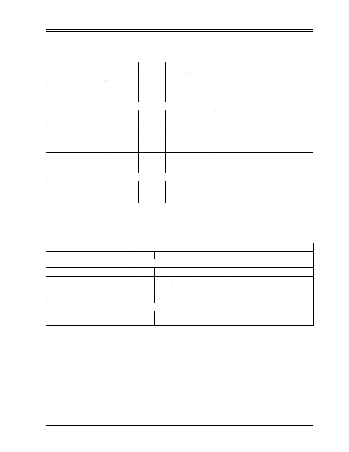
FIGURE 2-1:
Input Quiescent Current vs.
Input Voltage.
FIGURE 2-2:
Input Quiescent Current vs.
Temperature.
FIGURE 2-3:
Relative Oscillator
Frequency Variation vs. Temperature.
FIGURE 2-4:
+V
CC-OUT
Regulation vs.
Input Voltage.
FIGURE 2-5:
+V
CC-OUT
Regulation vs.
Load Current.
FIGURE 2-6:
LDO Regulator Dropout
Voltage vs. Temperature.
Note:
The graphs and tables provided following this note are a statistical summary based on a limited number of
samples and are provided for informational purposes only. The performance characteristics listed herein
are not tested or guaranteed. In some graphs or tables, the data presented may be outside the specified
operating range (e.g., outside specified power supply range) and therefore outside the warranted range.
5.0
6.0
7.0
iescent Current (mA)
f
SW
= 300 kHz
f
SW
= 600 kHz
4.0
0
5
10
15
20
25
30
35
Input Qu
Input Voltage (V)
4.0
6.0
8.0
10.0
iescent Current (mA)
0.0
2.0
-50
0
50
100
150
Input Qu
i
Junction Temperature (°C)
-4.0
-2.0
0.0
2.0
4.0
O
scillator Frequency
V
ariation (%
)
f
SW
= 300 kHz
f
SW
= 600 kHz
-10.0
-8.0
-6.0
-50
0
50
100
150
Relative
O
V
Junction Temperature (°C)
4.99
5.01
5.03
5.05
O
utput V
o
ltage (V)
I
LOAD
= 20 mA
4.95
4.97
0
10
20
30
40
LDO
O
Input Voltage (V)
4.99
5.01
5.03
5.05
Output V
o
ltage (V)
4.95
4.97
0
20
40
60
LDO
Load Current (mA)
0 5
0.75
1
1.25
1.5
ropout V
o
ltage (V)
I
LOAD
= 50 mA
0
0.25
0.5
-50
0
50
100
150
LDO D
r
Junction Temperature (°C)
MCP19035
DS22326B-page 8
2012-2013 Microchip Technology Inc.
Note:
Unless otherwise indicated, T
A
= +25°C, V
IN
= 12V, V
OUT
= 1.8V, f
SW
= 300 kHz, C
VCC
= 4.7 uF.
FIGURE 2-7:
+V
CC-OUT
LDO PSRR vs.
Frequency.
FIGURE 2-8:
Relative Reference Voltage
Variation vs. Temperature.
FIGURE 2-9:
UVLO Thresholds vs.
Temperature.
FIGURE 2-10:
Soft Start Time vs.
Temperature.
FIGURE 2-11:
High-Side Overcurrent
Threshold vs. Temperature.
FIGURE 2-12:
Low-Side Overcurrent
Threshold vs. Temperature.
-50.0
-30.0
-10.0
L
DO PSRR
(dB)
-90.0
-70.0
10
1000
100000
L
Frequency (Hz)
0
0.1
0.2
v
e Reference
V
o
ltage
V
a
riation (%
)
-0.2
-0.1
-50
0
50
100
150
Relati
v
Junction Temperature (°C)
3
4
5
V
o
latge Lockout
h
resholds (V)
V
IN
Rising
V
IN
Falling
2
3
-50
0
50
100
150
Under
T
h
Junction Temperature (°C)
8.0
9.0
10.0
11.0
12.0
t Start
T
ime (ms)
I
OUT
= 1 A
f
SW
= 600 kHz
f
SW
= 300 kHz
5.0
6.0
7.0
-50
0
50
100
150
Sof
t
Junction Temperature (°C)
f
SW
300 kHz
400
500
600
Side Overcurrent
h
reshold (mV)
V
CBOOT
= 5V
300
400
-50
0
50
100
150
High-
T
h
Junction Temperature (°C)
-100
0
-Side Overcurrent
hreshold (mV)
-200
-50
0
50
100
150
Low
-
T
Junction Temperature (°C)
2012-2013 Microchip Technology Inc.
DS22326B-page 9
MCP19035
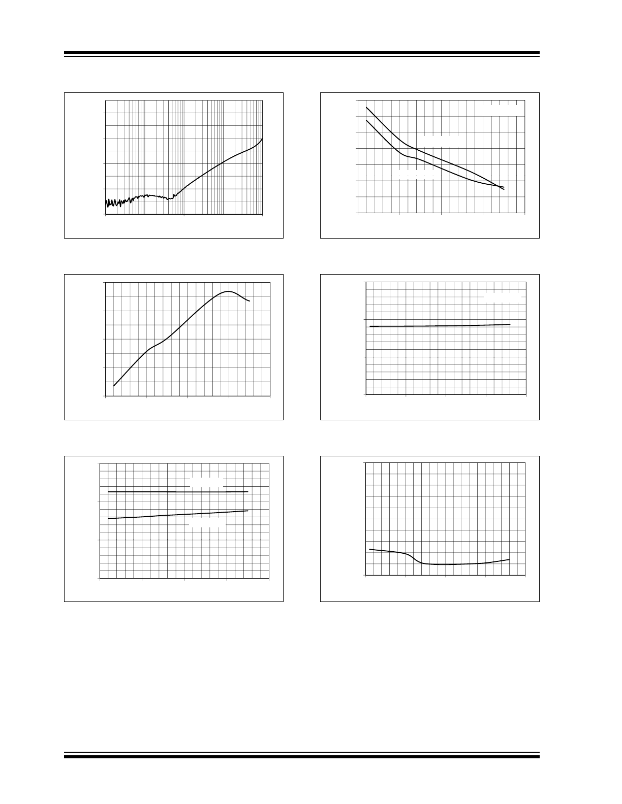
Note:
Unless otherwise indicated, T
A
= +25°C, V
IN
= 12V, V
OUT
= 1.8V, f
SW
= 300 kHz, C
VCC
= 4.7 uF.
FIGURE 2-13:
HDRV P-Ch R
DSon
Relative
Variation vs. Temperature.
FIGURE 2-14:
HDRV N-Ch R
DSon
Relative
Variation vs. Temperature.
FIGURE 2-15:
LDRV P-Ch R
DSon
Relative
Variation vs. Temperature.
FIGURE 2-16:
LDRV N-Ch R
DSon
Relative
Variation vs. Temperature
FIGURE 2-17:
PG Active Time Out Period
vs. Temperature.
FIGURE 2-18:
PG Thresholds Voltage vs.
Temperature.
20
-10
0
10
20
30
40
50
d
e Driver PMOS R
DSon
tive V
a
riation (%
)
-50
-40
-30
-20
-50
0
50
100
150
High-Si
d
Rela
t
Junction Temperature (°C)
-10
0
10
20
30
40
50
e
Driver NMOS R
DSon
tive V
a
riation (%
)
-50
-40
-30
-20
-50
0
50
100
150
High-Sid
e
Rela
t
Junction Temperature (°C)
-10
0
10
20
30
40
50
e
Driver PMOS R
DSon
tive V
a
riation (%
)
-50
-40
-30
-20
-50
0
50
100
150
Low
-Sid
e
Relea
t
Junction Temperature (°C)
-10
0
10
20
30
40
50
e
Driver NMOS R
DSon
tive V
a
riation (%
)
-50
-40
-30
-20
-50
0
50
100
150
Low
-Sid
e
Rela
t
Junction Temperature (°C)
120
130
140
150
G
ood Active
T
imeout
(ms)
100
110
-50
0
50
100
150
Pow
er
G
Junction Temperature (°C)
90
100
Good Thresholds
R
eference V
o
ltage)
PWRGD = Low
PWRGD = High
80
-50
0
50
100
150
Pow
e
(%
of
R
Junction Temperature (°C)

MCP19035
DS22326B-page 10
2012-2013 Microchip Technology Inc.
NOTES: