
2006-2013 Microchip Technology Inc.
DS22001D-page 1
MCP1827/MCP1827S
Features:
• 1.5A Output Current Capability
• Input Operating Voltage Range: 2.3V to 6.0V
• Adjustable Output Voltage Range: 0.8V to 5.0V
(MCP1827 only)
• Standard Fixed Output Voltages:
- 0.8V, 1.2V, 1.8V, 2.5V, 3.0V, 3.3V, 5.0V
• Other Fixed Output Voltage Options Available
Upon Request
• Low Dropout Voltage: 330 mV Typical at 1.5A
• Typical Output Voltage Tolerance: 0.5%
• Stable with 1.0 µF Ceramic Output Capacitor
• Fast response to Load Transients
• Low Supply Current: 120 µA (typ)
• Low Shutdown Supply Current: 0.1 µA (typ)
(MCP1827 only)
• Fixed Delay on Power Good Output
(MCP1827 only)
• Short Circuit Current Limiting and
Overtemperature Protection
• 5-Lead Plastic DDPAK, 5-Lead TO-220 Package
Options (MCP1827)
• 3-Lead Plastic DDPAK, 3-Lead TO-220 Package
Options (MCP1827S)
Applications:
• High-Speed Driver Chipset Power
• Networking Backplane Cards
• Notebook Computers
• Network Interface Cards
• Palmtop Computers
• 2.5V to 1.XV Regulators
Description:
The MCP1827/MCP1827S is a 1.5A Low Dropout
(LDO) linear regulator that provides high current and
low output voltages. The MCP1827 comes in a fixed or
adjustable output voltage version, with an output
voltage range of 0.8V to 5.0V. The 1.5A output current
capability, combined with the low output voltage
capability, make the MCP1827 a good choice for new
sub-1.8V output voltage LDO applications that have
high current demands. The MCP1827S is a 3-pin fixed
voltage version. The MCP1827/MCP1827S is based
upon the MCP1727 LDO device.
The MCP1827/MCP1827S is stable using ceramic
output capacitors that inherently provide lower output
noise and reduce the size and cost of the entire
regulator solution. Only 1 µF of output capacitance is
needed to stabilize the LDO.
Using CMOS construction, the quiescent current
consumed by the MCP1827/MCP1827S is typically
less than 120 µA over the entire input voltage range,
making it attractive for portable computing applications
that demand high output current. The MCP1827
versions have a Shutdown (SHDN) pin. When shut
down, the quiescent current is reduced to less than
0.1 µA.
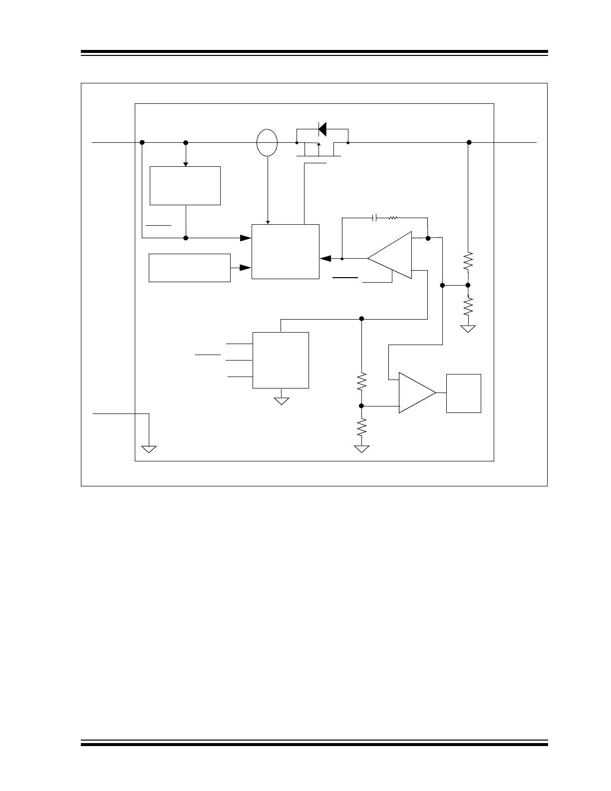
On the MCP1827 fixed output versions the scaled-
down output voltage is internally monitored and a
power good (PWRGD) output is provided when the
output is within 92% of regulation (typical). The
PWRGD delay is internally fixed at 200 µs (typical).
The overtemperature and short circuit current-limiting
provide additional protection for the LDO during system
Fault conditions.
Package Types
Fixed/Adjustable
3-LD DDPAK
5-LD DDPAK
3-LD TO-220
5-LD TO-220
1 2 3 4 5
1 2 3 4 5
1 2 3
1
2
3
PWRG
D
SHDN
V
IN
GND(
TA
B)
V
OU
T
ADJ
SHDN
V
IN
GND(
TAB) V
OU
T
V
IN
G
N
D(
TAB)
V
OU
T
V
IN
GND(
TAB)
V
OU
T
MCP1827
MCP1827
MCP1827S
MCP1827S
1.5A, Low-Voltage, Low Quiescent Current LDO Regulator
MCP1827/MCP1827S
DS22001D-page 2
2006-2013 Microchip Technology Inc.
Typical Application
MCP1827 Adjustable Output Voltage
MCP1827 Fixed Output Voltage
V
OUT
= 1.8V @ 1A
V
IN
= 2.3V to 2.8V
On
Off
1 µF
100 k
4.7 µF
C
1
C
2
R
1
SHDN
V
IN
GND
V
OUT
PWRGD
20 k
R
2
VADJ
1 2 3 4 5
V
OUT
= 1.2V @ 1A
V
IN
= 2.3V to 2.8V
On
Off
1 µF
40 k
4.7 µF
C
1
C
2
R
1
SHDN
V
IN
GND
V
OUT
1 2 3 4 5
2006-2013 Microchip Technology Inc.
DS22001D-page 3
MCP1827/MCP1827S
Functional Block Diagram – Adjustable Output
EA
+
–
V
OUT
PMOS
R
f
C
f
I
SNS
Overtemperature
V
REF
Comp
92% of V
REF
T
DELAY
V
IN
Driver w/limit
and SHDN
GND
Soft-Start
ADJ
Undervoltage
Lock Out
VIN
Reference
SHDN
SHDN
SHDN
Sensing
(UVLO)
MCP1827/MCP1827S
DS22001D-page 4
2006-2013 Microchip Technology Inc.
Functional Block Diagram – Fixed Output (5-pin)
EA
+
–
V
OUT
PMOS
R
f
C
f
I
SNS
V
REF
Comp
92% of V
REF
T
DELAY
V
IN
GND
Soft-Start
Sense
VIN
Reference
SHDN
SHDN
SHDN
PWRGD
Overtemperature
Driver w/limit
and SHDN
Undervoltage
Lock Out
Sensing
(UVLO)
2006-2013 Microchip Technology Inc.
DS22001D-page 5
MCP1827/MCP1827S
Functional Block Diagram – Fixed Output (3-Pin)
EA
+
–
V
OUT
PMOS
R
f
C
f
I
SNS
V
REF
Comp
92% of V
REF
T
DELAY
V
IN
GND
Soft-Start
Sense
V
IN
Reference
SHDN
SHDN
SHDN
Overtemperature
Driver w/limit
and SHDN
Undervoltage
Lock Out
Sensing
(UVLO)
MCP1827/MCP1827S
DS22001D-page 6
2006-2013 Microchip Technology Inc.
1.0
ELECTRICAL
CHARACTERISTICS
Absolute Maximum Ratings †
V
IN
....................................................................................6.5V
Maximum Voltage on Any Pin .. (GND – 0.3V) to (V
DD
+ 0.3)V
Maximum Power Dissipation......... Internally-Limited (
Note 6
)
Output Short Circuit Duration ................................Continuous
Storage temperature .....................................-65°C to +150°C
Maximum Junction Temperature, T
J
........................... +150°C
ESD protection on all pins (HBM/MM)
2 kV;
200V
† Notice: Stresses above those listed under “Maximum Rat-
ings” may cause permanent damage to the device. This is a
stress rating only and functional operation of the device at
those or any other conditions above those indicated in the
operational listings of this specification is not implied. Expo-
sure to maximum rating conditions for extended periods may
affect device reliability.
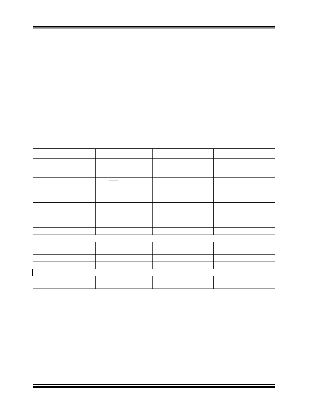
AC/DC CHARACTERISTICS
Electrical Specifications: Unless otherwise noted, V
IN
= V
OUT(MAX)
+ V
DROPOUT(MAX)
Note 1
, V
R
=1.8V for Adjustable Output,
I
OUT
= 1 mA, C
IN
= C
OUT
= 4.7 µF (X7R Ceramic), T
A
= +25°C. Boldface type applies for junction temperatures, T
J
(
Note 7
) of
-40°C to +125°C
Parameters
Sym.
Min.
Typ.
Max.
Units
Conditions
Input Operating Voltage
V
IN
2.3
6.0
V
Input Quiescent Current
I
q
—
120
220
µA
I
L
= 0 mA,
V
OUT
= 0.8V to 5.0V
Input Quiescent Current for
SHDN Mode
I
SHDN
—
0.1
3
µA
SHDN = GND
Maximum Output Current
I
OUT
1.5
—
—
A
V
IN
= 2.3V to 6.0V
V
R
= 0.8V to 5.0V
Line Regulation
V
OUT
/
(V
OUT
x
V
IN
)
—
0.05
0.16
%/V
(
Note 1
)
V
IN
6V
Load Regulation
V
OUT
/V
OUT
-1.0
±0.5
1.0
%
I
OUT
= 1 mA to 1.5A
(
Note 4
)
Output Short Circuit Current
I
OUT_SC
—
2.2
—
A
R
LOAD
< 0.1
, Peak Current
Adjust Pin Characteristics (Adjustable Output Only)
Adjust Pin Reference Voltage
V
ADJ
0.402
0.410
0.418
V
V
IN
= 2.3V to V
IN
= 6.0V,
I
OUT
= 1 mA
Adjust Pin Leakage Current
I
ADJ
-10
±0.01
+10
nA
V
IN
= 6.0V, V
ADJ
= 0V to 6V
Adjust Temperature Coefficient
TCV
OUT
—
40
—
ppm/°C
Note 3
Fixed-Output Characteristics (Fixed Output Only)
Voltage Regulation
V
OUT
V
R
- 2.5%
V
R
±0.5%
V
R
+ 2.5%
V
Note 2
Note 1:
The minimum V
IN
must meet two conditions: V
IN
2.3V and V
IN
V
OUT(MAX)
V
DROPOUT(MAX).
2:
V
R
is the nominal regulator output voltage for the fixed cases. V
R
= 1.2V, 1.8V, etc. V
R
is the desired set point output
voltage for the adjustable cases. V
R
= V
ADJ
*
((R
1
/R
2
)+1).
Figure 4-1
.
3:
TCV
OUT
= (V
OUT-HIGH
– V
OUT-LOW
) *10
6
/ (V
R
*
Temperature). V
OUT-HIGH
is the highest voltage measured over the
temperature range. V
OUT-LOW
is the lowest voltage measured over the temperature range.
4:
Load regulation is measured at a constant junction temperature using low duty-cycle pulse testing. Load regulation is
tested over a load range from 1 mA to the maximum specified output current.
5:
Dropout voltage is defined as the input-to-output voltage differential at which the output voltage drops 2% below its
nominal value that was measured with an input voltage of V
IN =
V
OUTMAX
+ V
DROPOUT(MAX)
.
6:
The maximum allowable power dissipation is a function of ambient temperature, the maximum allowable junction
temperature and the thermal resistance from junction to air. (i.e., T
A
, T
J
,
JA
). Exceeding the maximum allowable power
dissipation will cause the device operating junction temperature to exceed the maximum +150°C rating. Sustained
junction temperatures above 150°C can impact device reliability.
7:
The junction temperature is approximated by soaking the device under test at an ambient temperature equal to the
desired junction temperature. The test time is small enough such that the rise in the junction temperature over the
ambient temperature is not significant.
2006-2013 Microchip Technology Inc.
DS22001D-page 7
MCP1827/MCP1827S
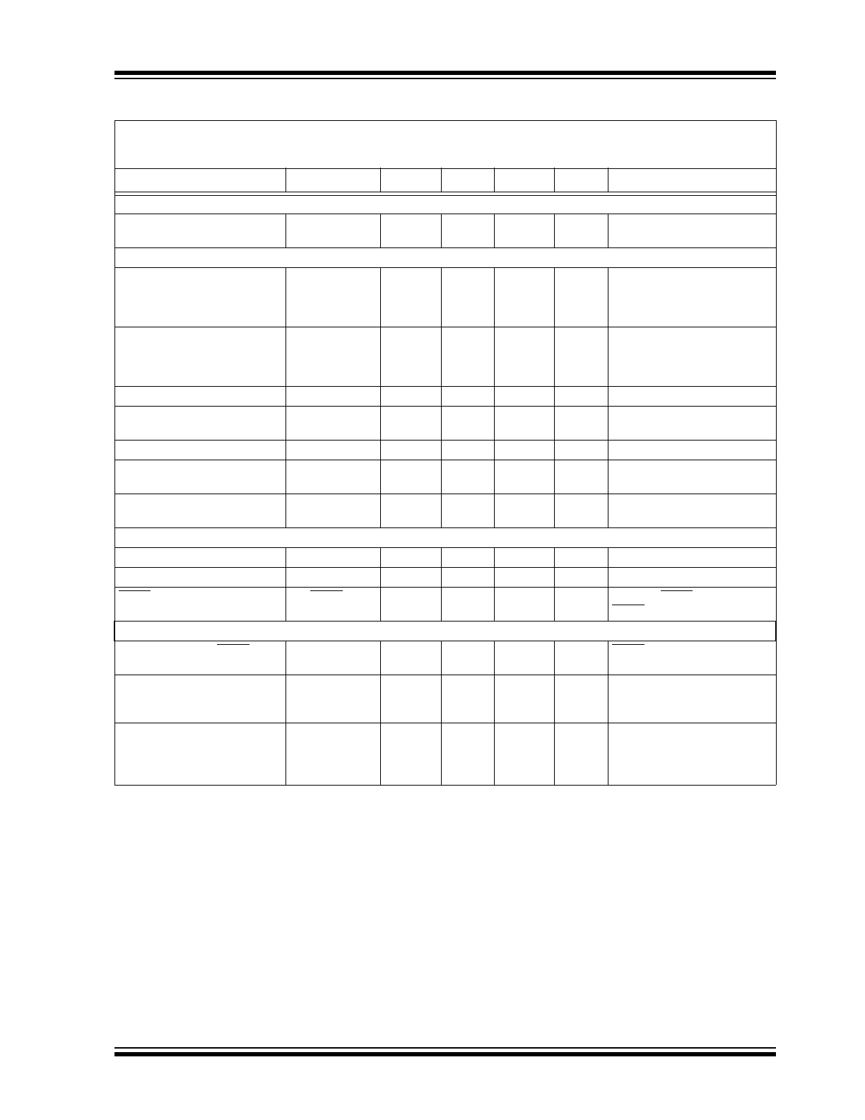
Dropout Characteristics
Dropout Voltage
V
IN
-V
OUT
—
330
600
mV
Note 5
, I
OUT
= 1.5A,
V
IN(MIN)
= 2.3V
Power Good Characteristics
PWRGD Input Voltage Operat-
ing Range
V
PWRGD_VIN
1.0
—
6.0
V
T
A
= +25°C
1.2
—
6.0
T
A
= -40°C to +125°C
For V
IN
< 2.3V, I
SINK
= 100 µA
PWRGD Threshold Voltage
(Referenced to V
OUT
)
V
PWRGD_TH
%V
OUT
Falling Edge
89
92
95
V
OUT
< 2.5V Fixed, V
OUT
= Adj.
90
92
94
V
OUT
>= 2.5V Fixed
PWRGD Threshold Hysteresis
V
PWRGD_HYS
1.0
2.0
3.0
%V
OUT
PWRGD Output Voltage Low
V
PWRGD_L
—
0.2
0.4
V
I
PWRGD
SINK
= 1.2 mA,
ADJ = 0V
PWRGD Leakage
P
WRGD
_
LK
—
1
—
nA
V
PWRGD
= V
IN
= 6.0V
PWRGD Time Delay
T
PG
—
200
—
µs
Rising Edge
R
PULLUP
= 10 k
Detect Threshold to PWRGD
Active Time Delay
T
VDET-PWRGD
—
200
—
µs
V
ADJ
or V
OUT
= V
PWRGD_TH
+
20 mV to V
PWRGD_TH
- 20 mV
Shutdown Input
Logic High Input
V
SHDN-HIGH
45
%V
IN
V
IN
= 2.3V to 6.0V
Logic Low Input
V
SHDN-LOW
15
%V
IN
V
IN
= 2.3V to 6.0V
SHDN Input Leakage Current
SHDN
ILK
-0.1
±0.001
+0.1
µA
V
IN
= 6V, SHDN =V
IN
,
SHDN = GND
AC Performance
Output Delay From SHDN
T
OR
100
µs
SHDN = GND to V
IN
V
OUT
= GND to 95% V
R
Output Noise
e
N
—
2.0
—
µV/
Hz I
OUT
= 200 mA, f = 1 kHz, C
OUT
= 10 µF (X7R Ceramic), V
OUT
=
2.5V
Power Supply Ripple Rejection
Ratio
PSRR
—
60
—
dB
f = 100 Hz, C
OUT
= 10 µF,
I
OUT
= 10 mA,
V
INAC
= 30 mV pk-pk,
C
IN
= 0 µF
AC/DC CHARACTERISTICS (CONTINUED)
Electrical Specifications: Unless otherwise noted, V
IN
= V
OUT(MAX)
+ V
DROPOUT(MAX)
Note 1
, V
R
=1.8V for Adjustable Output,
I
OUT
= 1 mA, C
IN
= C
OUT
= 4.7 µF (X7R Ceramic), T
A
= +25°C. Boldface type applies for junction temperatures, T
J
(
Note 7
) of
-40°C to +125°C
Parameters
Sym.
Min.
Typ.
Max.
Units
Conditions
Note 1:
The minimum V
IN
must meet two conditions: V
IN
2.3V and V
IN
V
OUT(MAX)
V
DROPOUT(MAX).
2:
V
R
is the nominal regulator output voltage for the fixed cases. V
R
= 1.2V, 1.8V, etc. V
R
is the desired set point output
voltage for the adjustable cases. V
R
= V
ADJ
*
((R
1
/R
2
)+1).
Figure 4-1
.
3:
TCV
OUT
= (V
OUT-HIGH
– V
OUT-LOW
) *10
6
/ (V
R
*
Temperature). V
OUT-HIGH
is the highest voltage measured over the
temperature range. V
OUT-LOW
is the lowest voltage measured over the temperature range.
4:
Load regulation is measured at a constant junction temperature using low duty-cycle pulse testing. Load regulation is
tested over a load range from 1 mA to the maximum specified output current.
5:
Dropout voltage is defined as the input-to-output voltage differential at which the output voltage drops 2% below its
nominal value that was measured with an input voltage of V
IN =
V
OUTMAX
+ V
DROPOUT(MAX)
.
6:
The maximum allowable power dissipation is a function of ambient temperature, the maximum allowable junction
temperature and the thermal resistance from junction to air. (i.e., T
A
, T
J
,
JA
). Exceeding the maximum allowable power
dissipation will cause the device operating junction temperature to exceed the maximum +150°C rating. Sustained
junction temperatures above 150°C can impact device reliability.
7:
The junction temperature is approximated by soaking the device under test at an ambient temperature equal to the
desired junction temperature. The test time is small enough such that the rise in the junction temperature over the
ambient temperature is not significant.
MCP1827/MCP1827S
DS22001D-page 8
2006-2013 Microchip Technology Inc.
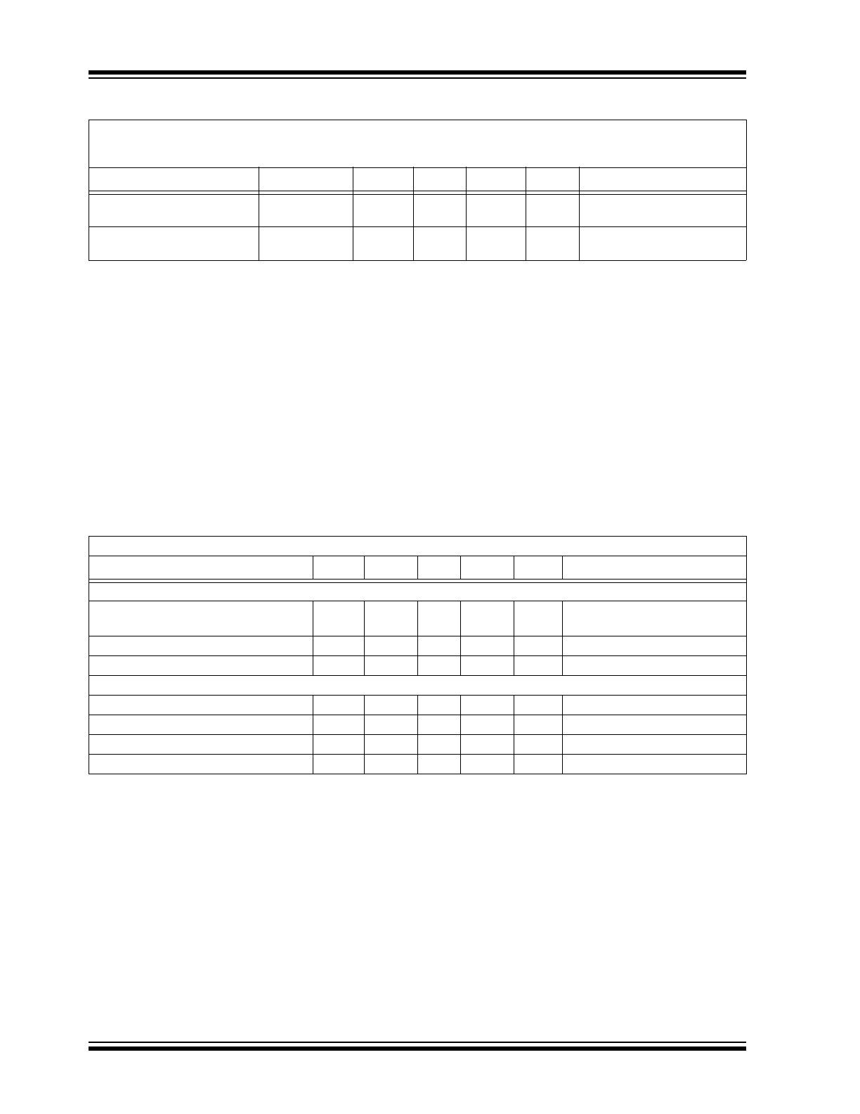
TEMPERATURE SPECIFICATIONS
Thermal Shutdown Temperature
T
SD
—
150
—
°C
I
OUT
= 100 µA, V
OUT
= 1.8V,
V
IN
= 2.8V
Thermal Shutdown Hysteresis
T
SD
—
10
—
°C
I
OUT
= 100 µA, V
OUT
= 1.8V,
V
IN
= 2.8V
Electrical Specifications: Unless otherwise indicated, all limits apply for V
IN
= 2.3V to 6.0V.
Parameters
Sym.
Min.
Typ.
Max.
Units
Conditions
Temperature Ranges
Operating Junction Temperature
Range
T
J
-40
—
+125
°C
Steady State
Maximum Junction Temperature
T
J
—
—
+150
°C
Transient
Storage Temperature Range
T
A
-65
—
+150
°C
Thermal Package Resistances
Thermal Resistance, 5LD DDPAK
JA
—
31.2
—
°C/W 4-Layer JC51 Standard Board
Thermal Resistance, 3LD DDPAK
JA
—
31.4
—
°C/W 4-Layer JC51 Standard Board
Thermal Resistance, 5LD TO-220
JA
—
29.3
—
°C/W 4-Layer JC51 Standard Board
Thermal Resistance, 3LD TO-220
JA
—
29.4
—
°C/W 4-Layer JC51 Standard Board
AC/DC CHARACTERISTICS (CONTINUED)
Electrical Specifications: Unless otherwise noted, V
IN
= V
OUT(MAX)
+ V
DROPOUT(MAX)
Note 1
, V
R
=1.8V for Adjustable Output,
I
OUT
= 1 mA, C
IN
= C
OUT
= 4.7 µF (X7R Ceramic), T
A
= +25°C. Boldface type applies for junction temperatures, T
J
(
Note 7
) of
-40°C to +125°C
Parameters
Sym.
Min.
Typ.
Max.
Units
Conditions
Note 1:
The minimum V
IN
must meet two conditions: V
IN
2.3V and V
IN
V
OUT(MAX)
V
DROPOUT(MAX).
2:
V
R
is the nominal regulator output voltage for the fixed cases. V
R
= 1.2V, 1.8V, etc. V
R
is the desired set point output
voltage for the adjustable cases. V
R
= V
ADJ
*
((R
1
/R
2
)+1).
Figure 4-1
.
3:
TCV
OUT
= (V
OUT-HIGH
– V
OUT-LOW
) *10
6
/ (V
R
*
Temperature). V
OUT-HIGH
is the highest voltage measured over the
temperature range. V
OUT-LOW
is the lowest voltage measured over the temperature range.
4:
Load regulation is measured at a constant junction temperature using low duty-cycle pulse testing. Load regulation is
tested over a load range from 1 mA to the maximum specified output current.
5:
Dropout voltage is defined as the input-to-output voltage differential at which the output voltage drops 2% below its
nominal value that was measured with an input voltage of V
IN =
V
OUTMAX
+ V
DROPOUT(MAX)
.
6:
The maximum allowable power dissipation is a function of ambient temperature, the maximum allowable junction
temperature and the thermal resistance from junction to air. (i.e., T
A
, T
J
,
JA
). Exceeding the maximum allowable power
dissipation will cause the device operating junction temperature to exceed the maximum +150°C rating. Sustained
junction temperatures above 150°C can impact device reliability.
7:
The junction temperature is approximated by soaking the device under test at an ambient temperature equal to the
desired junction temperature. The test time is small enough such that the rise in the junction temperature over the
ambient temperature is not significant.
2006-2013 Microchip Technology Inc.
DS22001D-page 9
MCP1827/MCP1827S
2.0
TYPICAL PERFORMANCE CURVES
Note: Unless otherwise indicated, V
OUT
= 1.8V (Adjustable), V
IN
= 2.8V, C
OUT
= 4.7 µF Ceramic (X7R), C
IN
= 4.7 µF
Ceramic (X7R), I
OUT
= 1 mA, Temperature = +25°C, V
IN
= V
OUT
+ 0.6V, R
PWRGD
= 10 k
To V
IN
.
Note: Junction Temperature (T
J
) is approximated by soaking the device under test to an ambient temperature equal to
the desired Junction temperature. The test time is small enough such that the rise in Junction temperature over the
Ambient temperature is not significant.
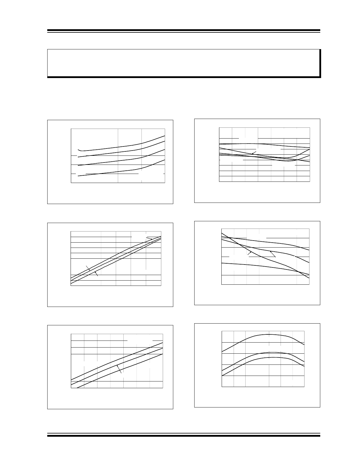
FIGURE 2-1:
Quiescent Current vs. Input
Voltage (1.2V Adjustable).
FIGURE 2-2:
Ground Current vs. Load
Current (1.2V Adjustable).
FIGURE 2-3:
Quiescent Current vs.
Junction Temperature (1.2V Adjustable).
FIGURE 2-4:
Line Regulation vs.
Temperature (1.2V Adjustable).
FIGURE 2-5:
Load Regulation vs.
Temperature (Adjustable Version).
FIGURE 2-6:
Adjust Pin Voltage vs.
Temperature.
Note:
The graphs and tables provided following this note are a statistical summary based on a limited number of
samples and are provided for informational purposes only. The performance characteristics listed herein
are not tested or guaranteed. In some graphs or tables, the data presented may be outside the specified
operating range (e.g., outside specified power supply range) and therefore outside the warranted range.
90
100
110
120
130
140
150
2
3
4
5
6
Input Voltage (V)
Q
u
ie
sc
en
t C
u
rr
en
t (
μ
A)
130
°C
-45
°C
25
°C
90
°C
V
OUT
= 1.2V Adj
I
OUT
= 0 mA
100
110
120
130
140
150
160
170
180
190
200
0
250
500
750
1000
1250
1500
Load Current (mA)
G
roun
d C
ur
rent
(µ
A
)
V
IN
=3.3V
V
OUT
= 1.2V Adj
V
IN
=5.0V
V
IN
=2.3V
100
105
110
115
120
125
130
135
140
-45
-20
5
30
55
80
105
130
Temperature (°C)
Q
u
ie
sc
en
t C
u
rr
en
t
(μ
A)
V
IN
=5.0V
V
IN
=2.5V
V
IN
=4.0V
I
OUT
= 0 mA
V
OUT
= 1.2V Adj
0
0.01
0.02
0.03
0.04
0.05
0.06
0.07
0.08
0.09
0.1
-45
-20
5
30
55
80
105
130
Temperature (°C)
Li
ne R
e
gul
ati
on (%/
V
)
V
OUT
= 1.2V adj
V
IN
= 2.3V to 6.0V
I
OUT
= 1 mA
I
OUT
= 500 mA
I
OUT
= 1000 mA
I
OUT
= 100 mA
-0.15
-0.10
-0.05
0.00
0.05
0.10
0.15
-45
-20
5
30
55
80
105
130
Temperature (°C)
L
o
ad R
e
gul
a
ti
o
n
(%
)
I
OUT
= 1.0 mA to 1500 mA
V
OUT
= 5.0V
V
OUT
= 3.3V
V
OUT
= 0.8V
V
OUT
= 1.8V
0.408
0.409
0.409
0.410
0.410
0.411
-45
-20
5
30
55
80
105
130
Temperature (°C)
A
d
ju
st
P
in V
o
lt
age
(V
)
I
OUT
= 1.0 mA
V
IN
= 6.0V
V
IN
= 2.3V
V
IN
= 5.0V
MCP1827/MCP1827S
DS22001D-page 10
2006-2013 Microchip Technology Inc.
Note: Unless otherwise indicated, V
OUT
= 1.8V (Adjustable), V
IN
= 2.8V, C
OUT
= 4.7 µF Ceramic (X7R), C
IN
= 4.7 µF
Ceramic (X7R), I
OUT
= 1 mA, Temperature = +25°C, V
IN
= V
OUT
+ 0.6V, R
PWRGD
= 10 k
To V
IN
.
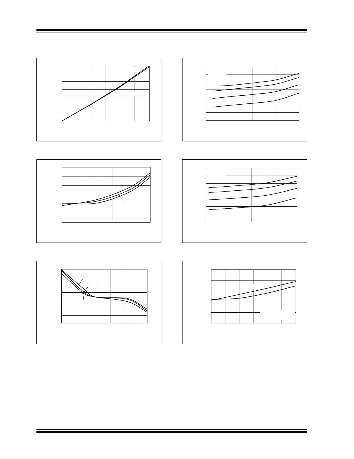
FIGURE 2-7:
Dropout Voltage vs. Load
Current (Adjustable Version).
FIGURE 2-8:
Dropout Voltage vs.
Temperature (Adjustable Version).
FIGURE 2-9:
Power Good (PWRGD)
Time Delay vs. Temperature (Adjustable
Version).
FIGURE 2-10:
Quiescent Current vs. Input
Voltage (0.8V Fixed).
FIGURE 2-11:
Quiescent Current vs. Input
Voltage (2.5V Fixed).
FIGURE 2-12:
Ground Current vs. Load
Current.
0.00
0.05
0.10
0.15
0.20
0.25
0.30
0.35
0
250
500
750
1000
1250
1500
Load Current (mA)
D
ro
pou
t V
o
lt
age
(V
)
V
OUT
= 2.5V Adj
V
OUT
= 5.0V Adj
0.30
0.32
0.34
0.36
0.38
0.40
0.42
-45
-20
5
30
55
80
105
130
Temperature (°C)
D
rop
out
Vo
lt
a
g
e (
V
)
V
OUT
= 3.3V Adj
V
OUT
= 5.0V Adj
V
OUT
= 2.5V Adj
I
OUT
= 1.5A
300
310
320
330
340
350
360
370
-45
-20
5
30
55
80
105
130
Temperature (°C)
P
o
we
r Go
o
d
T
im
e De
la
y
(µ
s
)
V
OUT
= 3.3V Fixed
V
IN
= 3.9V
V
IN
= 5.0V
V
IN
= 4.5V
80
90
100
110
120
130
140
150
2
3
4
5
6
Input Voltage (V)
Q
u
ies
cen
t C
u
rr
e
n
t (
μ
A)
-45°C
+130°C
+85°C
+25°C
V
OUT
= 0.8V
I
OUT
= 0 mA
80
90
100
110
120
130
140
150
3
3.5
4
4.5
5
5.5
6
Input Voltage (V)
Q
u
iesc
ent
C
u
rr
e
nt
(
μ
A)
V
OUT
= 2.5V
I
OUT
= 0 mA
+130
°C
-45
°C
+25
°C
+90
°C
0.00
50.00
100.00
150.00
200.00
250.00
0
250
500
750
1000
1250
1500
Load Current (mA)
G
round
C
u
rr
e
nt
(
μ
A)
V
IN
= 2.3V for V
R
=0.8V
V
IN
= 3.1V for V
R
=2.5V
V
OUT
=0.8V
V
OUT
=2.5V