

© 2010 Microchip Technology Inc.
DS22075B-page 1
MCP1790/MCP1791
Features
• 48V (43.5V ±10%) load dump protected for <500 ms
with a 30 second repetition rate (FORD Test Pulse
G Loaded)
• Wide steady state supply voltage, 6.0V - 30.0V
• Extended Junction Temperature Range:
-40 to +125°C
• Fixed output voltages: 3.0V, 3.3V, 5.0V
• Low quiescent current: 70 µA typical
• Low shutdown quiescent current: 10 µA typical
• Output Voltage Tolerances of ±2.5% over the
temperature range
• Maximum output current of 70 mA @ +125°C
Junction Temperature
• Maximum continuous input voltage of 30V
• Internal thermal overload protection, +157°C
(typical) Junction Temperature
• Internal short circuit current limit, 120 mA (typical)
for +5V option
• Short Circuit Current Foldback
• Shutdown Input option (MCP1791)
• Power Good Output option (MCP1791)
• High PSRR, -90 dB@100 Hz (typical)
• Stable with 1 µF to 1000 µF Tantalum and
Electrolytic Capacitors
• Stable with 4.7 µF to 1000 µF Ceramic Capacitors
Applications
• Low Voltage A/C powered (24VAC) Fire Alarms,
CO
2
Sensors, HVAC Controls
• Automotive Electronics
• Automotive Accessory Power Adapters
• Electronic Thermostat Controls
• Microcontroller power
General Description
The MCP1790/MCP1791 regulator provides up to 70 mA
of current. The input operating voltage range is specified
from 6.0V to 30V continuous, 48V absolute max, making
it ideal for automotive and commercial 12/24 VDC
systems.
The MCP1790/MCP1791 has a tight tolerance output
voltage load regulation of ±0.2% (typical) and a very
good line regulation at ±0.0002%/V (typical). The
regulator output is stable with ceramic, tantalum and
electrolytic capacitors. The MCP1790/MCP1791
regulator incorporates both thermal and short circuit
protection.
The MCP1790 is the 3-pin version of the MCP1790/
MCP1791 family. The MCP1791 is the 5-pin version
and incorporates a Shutdown input signal and a Power
Good output signal.
The regulator is specifically designed to operate in the
automotive environment and will survive +48V (43.5V
±10%) load dump transients and double-battery jumps.
The device is designed to meet the stringent quiescent
current requirements of the automotive industry. The
device is also designed for the commercial low voltage
fire alarm/detector systems, which use 24 VDC to
supply the required alarms throughout buildings. The
low ground current, 110 µA (typ.), of the CMOS device
will provide a power cost savings to the end users over
similar bipolar devices. Typical buildings using
hundreds of 24V powered fire and smoke detectors can
see substantial savings on energy consumption and
wiring gage reduction compared to bipolar regulators.
The MCP1790 device will be offered in the 3-pin
DD-PAK, and SOT-223 packages.
The MCP1791 device will be offered in the 5-pin
DD-PAK, and SOT-223 packages.
The MCP1790/MCP1791 will have a junction
temperature operating range of -40°C to +125°C.
70 mA, High Voltage Regulator
MCP1790/MCP1791
DS22075B-page 2
© 2010 Microchip Technology Inc.
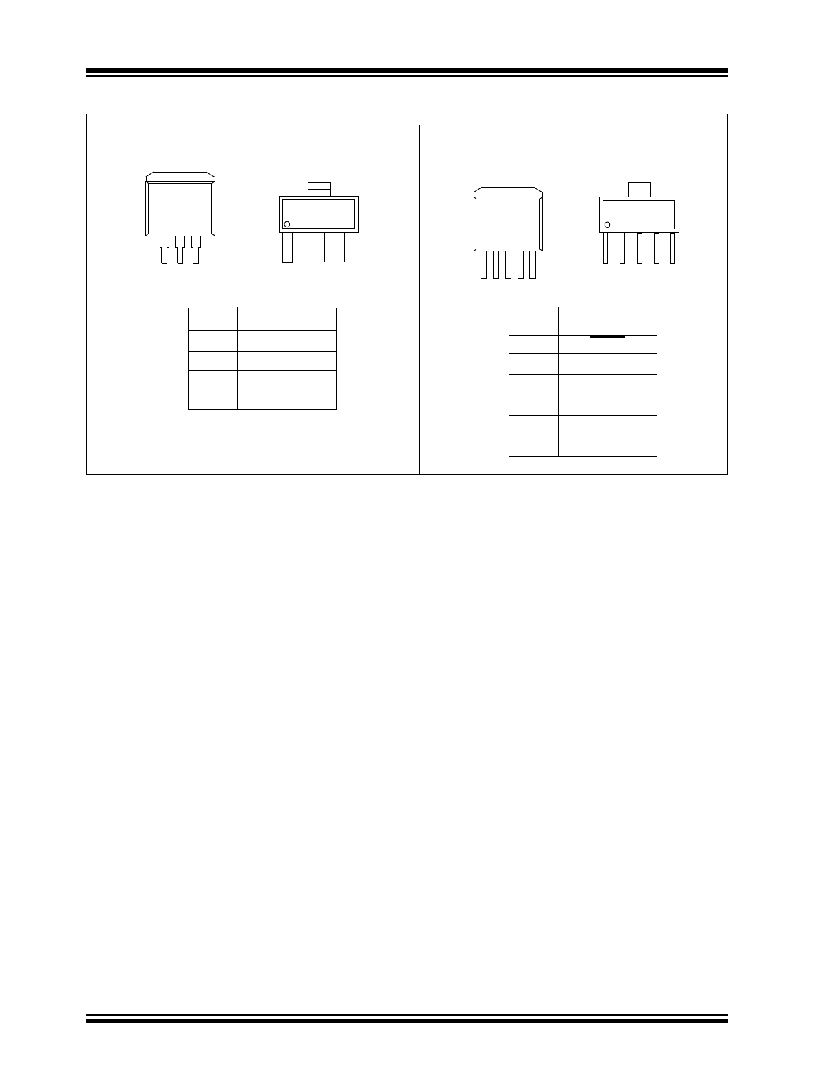
Package Types
MCP1791
1
2
3
4
5
6
SOT-223-5
Pin
1
SHDN
2
V
IN
3
GND (TAB)
4
V
OUT
5
PWRGD
6
GND (TAB)
1
2
3
SOT-223-3
4
MCP1790
Pin
1
V
IN
2
GND (TAB)
3
V
OUT
4
GND (TAB)
DDPAK-3
DDPAK-5
1 2 3 4 5
1 2 3
© 2010 Microchip Technology Inc.
DS22075B-page 3
MCP1790/MCP1791
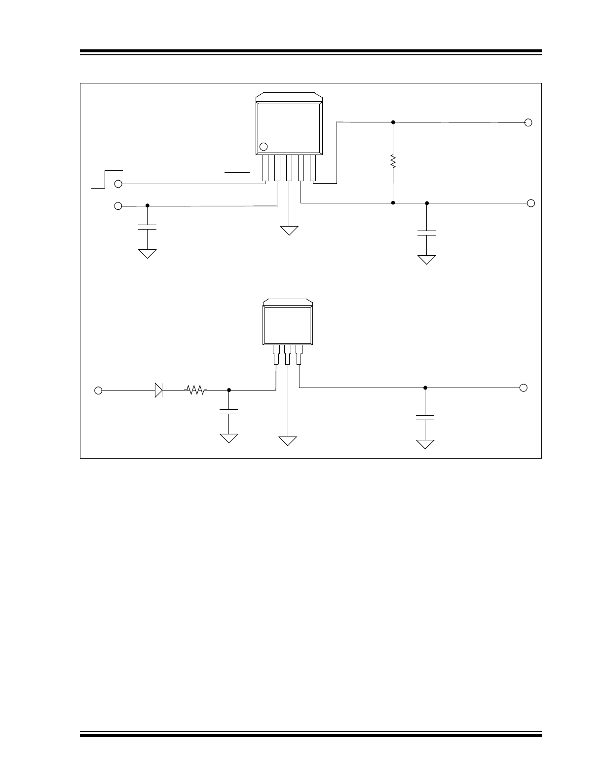
TYPICAL APPLICATION
V
OUT
= 5.0V @ 70 mA
V
IN
= 6V to 30V
On
Off
1 µF Tantalum
100 k
Ω
4.7 µF
C
1
C
2
R
1
SHDN
V
IN
GND
V
OUT
PWRGD
5
Ω
V
OUT
= 3.3V @ 70 mA
V
IN
= 8.0V to 16V
1.0 µF Tantalum
1.0 µF
C
1
C
2
V
IN
GND
V
OUT
1
1
MCP1791
MCP1790
MCP1790/MCP1791
DS22075B-page 4
© 2010 Microchip Technology Inc.
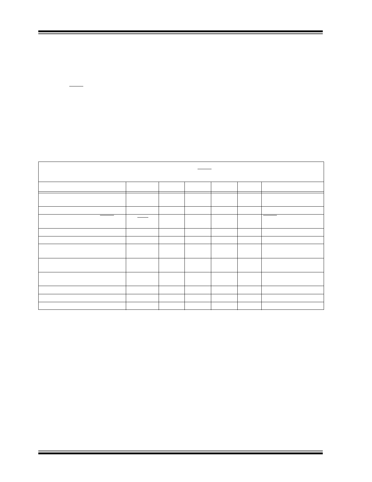
1.0
ELECTRICAL
CHARACTERISTICS
Absolute Maximum Ratings †
Input Voltage,
V
IN
........................................................+48.0V
V
IN
, PWRGD, SHDN ..................... (GND-0.3V) to (
V
IN
+0.3V)
V
OUT
.................................................... (GND-0.3V) to (+5.5V)
Internal Power Dissipation ............ Internally-Limited (Note 4)
Output Short Circuit Current..................................Continuous
Storage temperature .....................................-55°C to +150°C
Maximum Junction Temperature .....................165°C (Note 7)
Operating Junction Temperature...................-40°C to +125°C
ESD protection on all pins
........ ≥ 6 kV HBM and ≥ 400V MM
† Notice: Stresses above those listed under “Maximum Rat-
ings” may cause permanent damage to the device. This is a
stress rating only and functional operation of the device at
those or any other conditions above those indicated in the
operational listings of this specification is not implied. Expo-
sure to maximum rating conditions for extended periods may
affect device reliability.
AC/DC CHARACTERISTICS
Electrical Specifications: Unless otherwise noted, V
IN
= V
OUT(MAX)
+ V
DROPOUT(MAX),
(Note 1), I
OUT
= 1 mA,
C
OUT
= 4.7 µF (X7R Ceramic), C
IN
= 4.7 µF (X7R Ceramic), T
A
= +25°C, SHDN > 2.4V.
Boldface type applies for junction temperatures, T
J
(Note 5) of -40°C to +125°C.
Parameters
Symbol
Min
Typ
Max
Units
Conditions
Input Operating Voltage
V
IN
6.0
—
30.0
V
+48
V
DC
Load Dump Peak
< 500 ms
Input Quiescent Current
I
q
—
70
130
µA
I
L
= 0 mA
Input Quiescent Current for SHDN
Mode
I
SHDN
—
10
25
µA
SHDN = GND
Ground Current
I
GND
—
110
210
µA
I
L
= 70 mA
Maximum Output Current
I
OUT
70
—
—
mA
Line Regulation
ΔV
OUT
/
(V
OUT
X
ΔV
IN
)
—
±0.0002
±0.05
%/V
6.0V < V
IN
< 30V
Load Regulation
ΔV
OUT
/V
OUT
-0.45
±0.2
0.45
%
I
OUT
= 1 mA to 70 mA
(Note 3)
Output Peak Short Circuit Current
I
OUT_SC
—
V
R
/10
—
A
R
LOAD
< 0.1
Ω,
Peak Current
Output Voltage Regulation
V
OUT
V
R
-2.5%
V
R
V
R
+2.5%
V
—
V
OUT
Temperature Coefficient
TCV
OUT
—
65
—
ppm/°C
Note 9
Input Voltage to Turn On Output
V
ON
—
5.5
6.0
V
Rising V
IN
Note 1:
The minimum V
IN
, V
IN(MIN)
must meet two conditions: V
IN
≥ 6.0V and V
IN
≥ V
OUT(MAX)
+ V
DROPOUT(MAX).
2:
V
R
is the nominal regulator output voltage.
3:
Load regulation is measured at a constant junction temperature using low duty cycle pulse testing. Load regulation is
tested over a load range from 1 mA to the maximum specified output current.
4:
The maximum allowable power dissipation is a function of ambient temperature, the maximum allowable junction
temperature and the thermal resistance from junction to air. (i.e., T
A
, T
J
,
θ
JA
). Exceeding the maximum allowable power
dissipation will cause the device operating junction temperature to exceed the maximum 165°C rating. Sustained
junction temperatures above 165°C can impact the device reliability.
5:
The junction temperature is approximated by soaking the device under test at an ambient temperature equal to the
desired Junction temperature. The test time is small enough such that the rise in the Junction temperature over the
ambient temperature is not significant.
6:
Dropout voltage is defined as the input-to-output voltage differential at which the output voltage drops 2% below its
nominal value that was measured with an input voltage of V
IN
= V
R
+ V
DROPOUT(MAX)
.
7:
Sustained junction temperatures above 165°C can impact the device reliability.
8:
The Short Circuit Recovery Time test is done by placing the device into a short circuit condition and then removing the
short circuit condition before the device die temperature reaches 125 °C. If the device goes into thermal shutdown, then
the Short Circuit Recovery Time will depend upon the thermal dissipation properties of the package and circuit board.
9:
TCV
OUT
= (V
OUT-HIGH
- V
OUT-LOW
) *10^6/(V
R
*
ΔTemperature), V
OUT-HIGH
= highest voltage measured over the temperature
range. V
OUT-LOW
= lowest voltage measured over the temperature range.
© 2010 Microchip Technology Inc.
DS22075B-page 5
MCP1790/MCP1791
Short Circuit Foldback Voltage Corner
V
FOLDBACK
—
4.2
—
V
V
R
= 5.0V
Falling V
OUT,
R
LOAD
< 0.1
Ω
—
3.0
—
V
V
R
= 3.3V
Falling V
OUT,
R
LOAD
< 0.1
Ω
—
2.7
—
V
V
R
= 3.0V
Falling V
OUT,
R
LOAD
< 0.1
Ω
Short Circuit Foldback Current
—
105
—
mA
V
OUT
~= 0V,
R
LOAD
< 0.1
Ω,
V
R
= 5.0V (Note 2)
—
99
—
mA
V
R
= 3.3V (Note 2)
—
99
—
mA
V
R
= 3.0V (Note 2)
Startup Voltage Overshoot
V
OVER
—
0.10
—
% V
OUT
V
IN
= 0V to 6.0V
Dropout Voltage
V
DROPOUT
—
700
1300
mV
I
OUT
= 70 mA, (Note 6)
Dropout Current
I
OUT
= 0 mA
I
DO
—
130
—
µA
V
R
= 5.0V, V
IN
= 4.500V
—
75
—
µA
V
R
= 3.3V, V
IN
= 4.500V
—
75
—
µA
V
R
= 3.0V, V
IN
= 4.500V
Shutdown Input
Logic High Input
V
SHDN-HIGH
2.4
—
V
IN(MAX)
V
—
Logic Low Input
V
SHDN-LOW
0
—
0.8
V
—
Shutdown Input Leakage Current
SHDN
ILK
—
—
0.100
3.0
0.500
5.0
µA
SHDN = GND
SHDN = 6V
Power Good Characteristics
PWRGD Input Voltage Operating
Range
V
PWRGD_VIN
2.8
—
—
V
—
PWRGD Threshold Voltage
(Referenced to V
OUT
)
V
PWRGD_TH
88
90
92
%V
OUT
Falling Edge of V
OUT
PWRGD Threshold Hysteresis
V
PWRGD_HYS
1.0
2.0
3.0
%V
OUT
Rising Edge of V
OUT
PWRGD Output Voltage LOW
V
PWRGD_L
—
0.2
0.4
V
I
PWRGD
SINK
= 5.0 mA,
V
OUT
= 0V
PWRGD Output Sink Current
I
PWRGD_L
5.0
—
—
mA
V
PWRGD
<= 0.4V
PWRGD Leakage
I
PWRGD
_
LK
—
1.0
—
nA
V
PWRGD
= V
IN
= 6.0V
PWRGD Time Delay
T
PG
—
30
—
µs
Rising Edge
AC/DC CHARACTERISTICS (CONTINUED)
Electrical Specifications: Unless otherwise noted, V
IN
= V
OUT(MAX)
+ V
DROPOUT(MAX),
(Note 1), I
OUT
= 1 mA,
C
OUT
= 4.7 µF (X7R Ceramic), C
IN
= 4.7 µF (X7R Ceramic), T
A
= +25°C, SHDN > 2.4V.
Boldface type applies for junction temperatures, T
J
(Note 5) of -40°C to +125°C.
Parameters
Symbol
Min
Typ
Max
Units
Conditions
Note 1:
The minimum V
IN
, V
IN(MIN)
must meet two conditions: V
IN
≥ 6.0V and V
IN
≥ V
OUT(MAX)
+ V
DROPOUT(MAX).
2:
V
R
is the nominal regulator output voltage.
3:
Load regulation is measured at a constant junction temperature using low duty cycle pulse testing. Load regulation is
tested over a load range from 1 mA to the maximum specified output current.
4:
The maximum allowable power dissipation is a function of ambient temperature, the maximum allowable junction
temperature and the thermal resistance from junction to air. (i.e., T
A
, T
J
,
θ
JA
). Exceeding the maximum allowable power
dissipation will cause the device operating junction temperature to exceed the maximum 165°C rating. Sustained
junction temperatures above 165°C can impact the device reliability.
5:
The junction temperature is approximated by soaking the device under test at an ambient temperature equal to the
desired Junction temperature. The test time is small enough such that the rise in the Junction temperature over the
ambient temperature is not significant.
6:
Dropout voltage is defined as the input-to-output voltage differential at which the output voltage drops 2% below its
nominal value that was measured with an input voltage of V
IN
= V
R
+ V
DROPOUT(MAX)
.
7:
Sustained junction temperatures above 165°C can impact the device reliability.
8:
The Short Circuit Recovery Time test is done by placing the device into a short circuit condition and then removing the
short circuit condition before the device die temperature reaches 125 °C. If the device goes into thermal shutdown, then
the Short Circuit Recovery Time will depend upon the thermal dissipation properties of the package and circuit board.
9:
TCV
OUT
= (V
OUT-HIGH
- V
OUT-LOW
) *10^6/(V
R
*
ΔTemperature), V
OUT-HIGH
= highest voltage measured over the temperature
range. V
OUT-LOW
= lowest voltage measured over the temperature range.
MCP1790/MCP1791
DS22075B-page 6
© 2010 Microchip Technology Inc.
Detect Threshold to PWRGD Active
Time Delay
TV
DET-PWRG
D
—
235
—
µs
V
OUT
= V
PWRGD_TH
+
100 mV to V
PWRGD_TH
-
100 mV
AC Performance
Output Delay from SHDN
T
OR
—
200
—
µs
SHDN = GND to V
IN,
V
OUT
= GND to 95% V
R,
C
OUT
= 1.0 µF
PWRGD Delay from SHDN
T
SHDN_PG
—
400
—
ns
SHDN = V
IN
to GND
,
C
OUT
= 1.0 µF
Output Noise
e
N
—
1.2
—
(µV/
√Hz) I
OUT
= 50 mA, f = 1 kHz
Power Supply Ripple Rejection Ratio
PSRR
dB
V
IN
= 7.0V, C
IN
= 0 µF,
I
OUT
= 10 mA,
V
INAC
= 400 mVpp
—
90
—
f = 100 Hz
—
75
—
f = 1 kHz, V
R
= 5.0V
—
80
—
f = 1 kHz, V
R
= < 5.0V
Thermal Shutdown Temperature
T
SD
—
157
—
°C
Rising Temperature
Thermal Shutdown Hysteresis
ΔT
SD
—
20
—
°C
Falling Temperature
Short Circuit Recovery Time
t
THERM
—
0
—
ms
(Note 8)
AC/DC CHARACTERISTICS (CONTINUED)
Electrical Specifications: Unless otherwise noted, V
IN
= V
OUT(MAX)
+ V
DROPOUT(MAX),
(Note 1), I
OUT
= 1 mA,
C
OUT
= 4.7 µF (X7R Ceramic), C
IN
= 4.7 µF (X7R Ceramic), T
A
= +25°C, SHDN > 2.4V.
Boldface type applies for junction temperatures, T
J
(Note 5) of -40°C to +125°C.
Parameters
Symbol
Min
Typ
Max
Units
Conditions
Note 1:
The minimum V
IN
, V
IN(MIN)
must meet two conditions: V
IN
≥ 6.0V and V
IN
≥ V
OUT(MAX)
+ V
DROPOUT(MAX).
2:
V
R
is the nominal regulator output voltage.
3:
Load regulation is measured at a constant junction temperature using low duty cycle pulse testing. Load regulation is
tested over a load range from 1 mA to the maximum specified output current.
4:
The maximum allowable power dissipation is a function of ambient temperature, the maximum allowable junction
temperature and the thermal resistance from junction to air. (i.e., T
A
, T
J
,
θ
JA
). Exceeding the maximum allowable power
dissipation will cause the device operating junction temperature to exceed the maximum 165°C rating. Sustained
junction temperatures above 165°C can impact the device reliability.
5:
The junction temperature is approximated by soaking the device under test at an ambient temperature equal to the
desired Junction temperature. The test time is small enough such that the rise in the Junction temperature over the
ambient temperature is not significant.
6:
Dropout voltage is defined as the input-to-output voltage differential at which the output voltage drops 2% below its
nominal value that was measured with an input voltage of V
IN
= V
R
+ V
DROPOUT(MAX)
.
7:
Sustained junction temperatures above 165°C can impact the device reliability.
8:
The Short Circuit Recovery Time test is done by placing the device into a short circuit condition and then removing the
short circuit condition before the device die temperature reaches 125 °C. If the device goes into thermal shutdown, then
the Short Circuit Recovery Time will depend upon the thermal dissipation properties of the package and circuit board.
9:
TCV
OUT
= (V
OUT-HIGH
- V
OUT-LOW
) *10^6/(V
R
*
ΔTemperature), V
OUT-HIGH
= highest voltage measured over the temperature
range. V
OUT-LOW
= lowest voltage measured over the temperature range.
© 2010 Microchip Technology Inc.
DS22075B-page 7
MCP1790/MCP1791
TEMPERATURE SPECIFICATIONS
Parameters
Symbol
Min
Typ
Max
Units
Conditions
Temperature Ranges
Specified Temperature Range
T
J
-40
—
+125
°C
—
Operating Temperature Range
T
J
-40
—
+125
°C
—
Storage Temperature Range
T
A
-55
—
+150
°C
—
Package Thermal Resistances
Thermal Resistance, 3LD DDPAK
θ
JA
θ
JC
—
31.4
3
—
°C/W
EIA/JEDEC JESD51-751-7
4 Layer Board
Thermal Resistance, 3LD SOT-223
θ
JA
θ
JC
—
62
15
—
°C/W
EIA/JEDEC JESD51-751-7
4 Layer Board
Thermal Resistance, 5LD DDPAK
θ
JA
θ
JC
—
31.4
3
—
°C/W
EIA/JEDEC JESD51-751-7
4 Layer Board
Thermal Resistance, 5LD SOT-223
θ
JA
θ
JC
—
62
15
—
°C/W
EIA/JEDEC JESD51-751-7
4 Layer Board
MCP1790/MCP1791
DS22075B-page 8
© 2010 Microchip Technology Inc.
2.0
TYPICAL PERFORMANCE CHARACTERISTICS
Note:
Unless otherwise indicated, C
OUT
= 4.7 uF Ceramic (X7R), C
IN
= 10.0 µF Ceramic (X7R), I
OUT
= 1 mA, Temperature = +25°C,
V
IN
= 6.0V, R
PWRGD_PULLUP
= 10 k
Ω To V
OUT
, V
SHDN
= V
IN,
and device is MCP1790.
Note:
Junction Temperature (TJ) is approximated by soaking the device under test to an ambient temperature equal to the desired
junction temperature. The test time is small enough such that the rise in Junction Temperature over the Ambient temperature is not
significant.
FIGURE 2-1:
Power Good Time Delay vs.
Temperature (MCP1791).
FIGURE 2-2:
Quiescent Current vs. Input
Voltage.
FIGURE 2-3:
Quiescent Current vs. Input
Voltage.
FIGURE 2-4:
Quiescent Current vs.
Junction Temperature.
FIGURE 2-5:
Ground Current vs. Load
Current.
FIGURE 2-6:
I
SHDN
vs Temperature.
Note:
The graphs and tables provided following this note are a statistical summary based on a limited number of
samples and are provided for informational purposes only. The performance characteristics listed herein
are not tested or guaranteed. In some graphs or tables, the data presented may be outside the specified
operating range (e.g., outside specified power supply range) and therefore outside the warranted range.
0
10
20
30
40
50
-45
-20
5
30
55
80
105
130
Temperature (°C)
PWRGD Time
Dela
y (
µ
s)
V
OUT
= 5.0V
I
OUT
= 0 µA
V
IN
= 10V,15V,25V,30V
V
IN
= 6V
0
20
40
60
80
100
120
140
0
5
10
15
20
25
30
35
Input Voltage (V)
Quie
sc
ent
Current
(µ
A)
V
OUT
= 3.3V
I
OUT
= 0 µA
+25°C
+130°C
-45°C
0°C
+90°C
0
20
40
60
80
100
120
140
0
5
10
15
20
25
30
35
Input Voltage (V)
Quie
sc
ent
Current
(µ
A)
V
OUT
= 5.0V
I
OUT
= 0 µA
+25°C
+130°C
-45°C
0°C
+90°C
0.00
20.00
40.00
60.00
80.00
100.00
120.00
-45
-20
5
30
55
80
105
130
Junction Temperature (°C)
Quies
c
en
t Curre
nt (µA)
V
IN
= 6V
I
OUT
= 0µA
V
OUT
= 5.0V
V
OUT
= 3.3V
V
OUT
= 3.0V
0
20
40
60
80
100
120
140
0
10
20
30
40
50
60
70
Load Current (mA)
GND
Current (
µ
A)
V
OUT
= 5.0V
V
OUT
= 3.0V
V
OUT
= 3.3V
0
4
8
12
16
20
24
28
-45
-20
5
30
55
80
105
130
Temperature (°C)
I
SH
DN
(µ
A
)
V
IN
= 6.0V
V
IN
= 10V, 30V
V
REG
= 3.0V
V
SHDN
= 0V
© 2010 Microchip Technology Inc.
DS22075B-page 9
MCP1790/MCP1791
Note:
Unless otherwise indicated, C
OUT
= 4.7 uF Ceramic (X7R), C
IN
= 10.0 µF Ceramic (X7R), I
OUT
= 1 mA, Temperature = +25°C,
V
IN
= 6.0V, R
PWRGD_PULLUP
= 10 k
Ω To V
OUT
, V
SHDN
= V
IN,
and device is MCP1790.
FIGURE 2-7:
Line Regulation vs.
Temperature.
FIGURE 2-8:
Line Regulation vs.
Temperature.
FIGURE 2-9:
Load Regulation vs.
Temperature.
FIGURE 2-10:
Output Voltage vs. Load
Current.
FIGURE 2-11:
Dropout Voltage vs. Load
Current.
FIGURE 2-12:
Dropout Voltage vs.
Temperature.
-0.006
-0.004
-0.002
0.000
0.002
0.004
0.006
-45
-20
5
30
55
80
105
130
Temperature (°C)
Line Regulat
ion (%/V)
V
OUT
= 3.3V
V
IN
= 6V to 30V
70 mA
10 mA
0 mA
-0.006
-0.004
-0.002
0.000
0.002
0.004
0.006
-45
-20
5
30
55
80
105
130
Temperature (°C)
Line Regulat
ion (%/V)
V
OUT
= 5.0V
V
IN
= 6V to 30V
70 mA
0 mA
30 mA
-0.30
-0.25
-0.20
-0.15
-0.10
-0.05
0.00
-45
-20
5
30
55
80
105
130
Temperature (°C)
Load Regulation (
%
)
I
LOAD
= 1 mA to 70 mA
V
REG
=5.0V
V
REG
=3.3V
V
REG
=3.0V
4.94
4.95
4.96
4.97
4.98
4.99
5.00
5.01
5.02
5.03
5.04
0
10
20
30
40
50
60
70
Load Current (mA)
Output
V
o
lt
age (
V
)
V
OUT
= 5.0V
V
IN
= 6.3V
+25°C
+130°C
-45°C
0°C
+90°C
+25°C
+130°C
-45°C
0°C
+90°C
0.0
0.1
0.2
0.3
0.4
0.5
0.6
0.7
0.8
0.9
1.0
0
10
20
30
40
50
60
70
Load Current (mA)
Dropout Voltage (
V
)
V
OUT
= 5.0V
+25°C
+130°C
-45°C
0°C
+90°C
0.0
0.1
0.2
0.3
0.4
0.5
0.6
0.7
0.8
0.9
1.0
-45
-20
5
30
55
80
105
130
Temperature (°C)
Dropout Voltage (
V
)
V
OUT
= 5.0V
1 mA
50 mA
10 mA
30 mA
70 mA
MCP1790/MCP1791
DS22075B-page 10
© 2010 Microchip Technology Inc.
Note:
Unless otherwise indicated, C
OUT
= 4.7 uF Ceramic (X7R), C
IN
= 10.0 µF Ceramic (X7R), I
OUT
= 1 mA, Temperature = +25°C,
V
IN
= 6.0V, R
PWRGD_PULLUP
= 10 k
Ω To V
OUT
, V
SHDN
= V
IN,
and device is MCP1790.
FIGURE 2-13:
Short Circuit Current vs
Input Voltage.
FIGURE 2-14:
Output Noise Voltage
Density vs. Frequency.
FIGURE 2-15:
Power Supply Ripple
Rejection vs. Frequency.
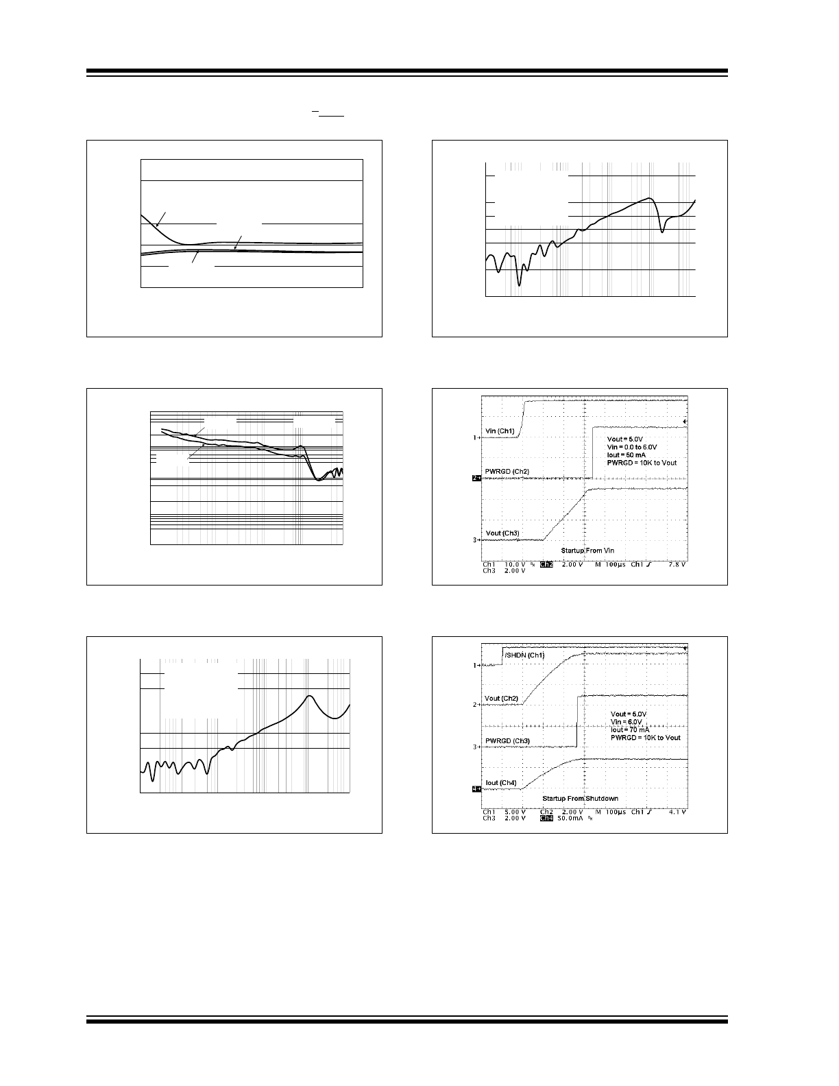
FIGURE 2-16:
Power Supply Ripple
Rejection vs. Frequency.
FIGURE 2-17:
Startup from V
IN
(MCP1791).
FIGURE 2-18:
Startup from Shutdown
(MCP1791).
100
105
110
115
120
125
130
6
10
14
18
22
26
30
Input Voltage (V)
S
hort
Circuit Current (
m
A)
R
OUT
< 0.1
Ω
V
OUT
= 5.0V
V
OUT
= 3.3V
V
OUT
= 3.0V
0.00
0.01
0.10
1.00
10.00
0.01
0.1
1
10
100
1000
Frequency (kHz)
Noise (μV/Hz)
V
R
=5.0V
I
OUT
=50mA
V
R
=3.3V
-110
-100
-90
-80
-70
-60
-50
-40
-30
-20
0.01
0.1
1
10
100
1000
Frequency (kHz)
PSRR (
d
B)
V
R
=3.3V
V
IN
=7.0V
V
INAC
= 400 mV p-p
C
IN
=0 μF
I
OUT
=10 mA
-120
-110
-100
-90
-80
-70
-60
-50
-40
-30
-20
0.01
0.1
1
10
100
1000
Frequency (kHz)
PSRR (dB)
V
R
=5.0V
V
IN
=7.0V
V
INAC
= 400 mV p-p
C
IN
=0 μF
I
OUT
=10 mA