

2011-2013 Microchip Technology Inc.
DS20002276C-page 1
MCP1754/MCP1754S
Features:
• High PSRR: >70 dB @ 1 kHz, Typical
• 56.0 µA Typical Quiescent Current
• Input Operating Voltage Range: 3.6V to16.0V
• 150 mA Output Current for All Output Voltages
• Low-Dropout Voltage, 300 mV Typical @ 150 mA
• 0.4% Typical Output Voltage Tolerance
• Standard Output Voltage Options (1.8V, 2.5V,
2.8V, 3.0V, 3.3V, 4.0V, 5.0V)
• Output Voltage Range 1.8V to 5.5V in 0.1V
Increments (tighter increments also possible per
design)
• Output Voltage Tolerances of ±2.0% Over Entire
Temperature Range
• Stable with Minimum 1.0 µF Output Capacitance
• Power Good Output
• Shutdown Input
• True Current Foldback Protection
• Short-Circuit Protection
• Overtemperature Protection
Applications:
• Battery-Powered Devices
• Battery-Powered Alarm Circuits
• Smoke Detectors
• CO
2
Detectors
• Pagers and Cellular Phones
• Smart Battery Packs
• PDAs
• Digital Cameras
• Microcontroller Power
• Consumer Products
• Battery-Powered Data Loggers
Related Literature:
• AN765, “Using Microchip’s Micropower LDOs”
(DS00765), Microchip Technology Inc., 2007
• AN766, “Pin-Compatible CMOS Upgrades to
BiPolar LDOs” (DS00766),
Microchip Technology Inc., 2003
• AN792, “A Method to Determine How Much
Power a SOT23 Can Dissipate in an Application”
(DS00792), Microchip Technology Inc., 2001
Description:
The MCP1754/MCP1754S is a family of CMOS low
dropout (LDO) voltage regulators that can deliver up to
150 mA of current while consuming only 56.0 µA of
quiescent current (typical). The input operating range is
specified from 3.6V to 16.0V, making it an ideal choice
for four to six primary cell battery-powered applications,
12V mobile applications and one to three-cell Li-Ion-
powered applications.
The MCP1754/MCP1754S is capable of delivering
150 mA with only 300 mV (typical) of input to output
voltage differential. The output voltage tolerance of the
MCP1754/MCP1754S is typically ±0.2% at +25°C and
±2.0% maximum over the operating junction
temperature range of -40°C to +125°C. Line regulation
is ±0.01% typical at +25°C.
Output voltages available for the MCP1754/MCP1754S
range from 1.8V to 5.5V. The LDO output is stable when
using only 1 µF of output capacitance. Ceramic,
tantalum or aluminum electrolytic capacitors may all be
used for input and output. Overcurrent limit and
overtemperature shutdown provide a robust solution for
any application.
The MCP1754/MCP1754S family introduces a true
current foldback feature. When the load impedance
decreases beyond the MCP1754/MCP1754S load
rating, the output current and voltage will gracefully
foldback towards 30 mA at about 0V output. When the
load impedance decreases and returns to the rated
load, the MCP1754/MCP1754S follows the same
foldback curve as the device comes out of current
foldback.
Package options for the MCP1754S include the
SOT-23A, SOT-89-3, SOT-223-3 and 2x3 DFN-8.
Package options for the MCP1754 include the
SOT-23-5, SOT-223-5, and 2x3 DFN-8.
150 mA, 16V, High-Performance LDO
MCP1754/MCP1754S
DS20002276C-page 2
2011-2013 Microchip Technology Inc.
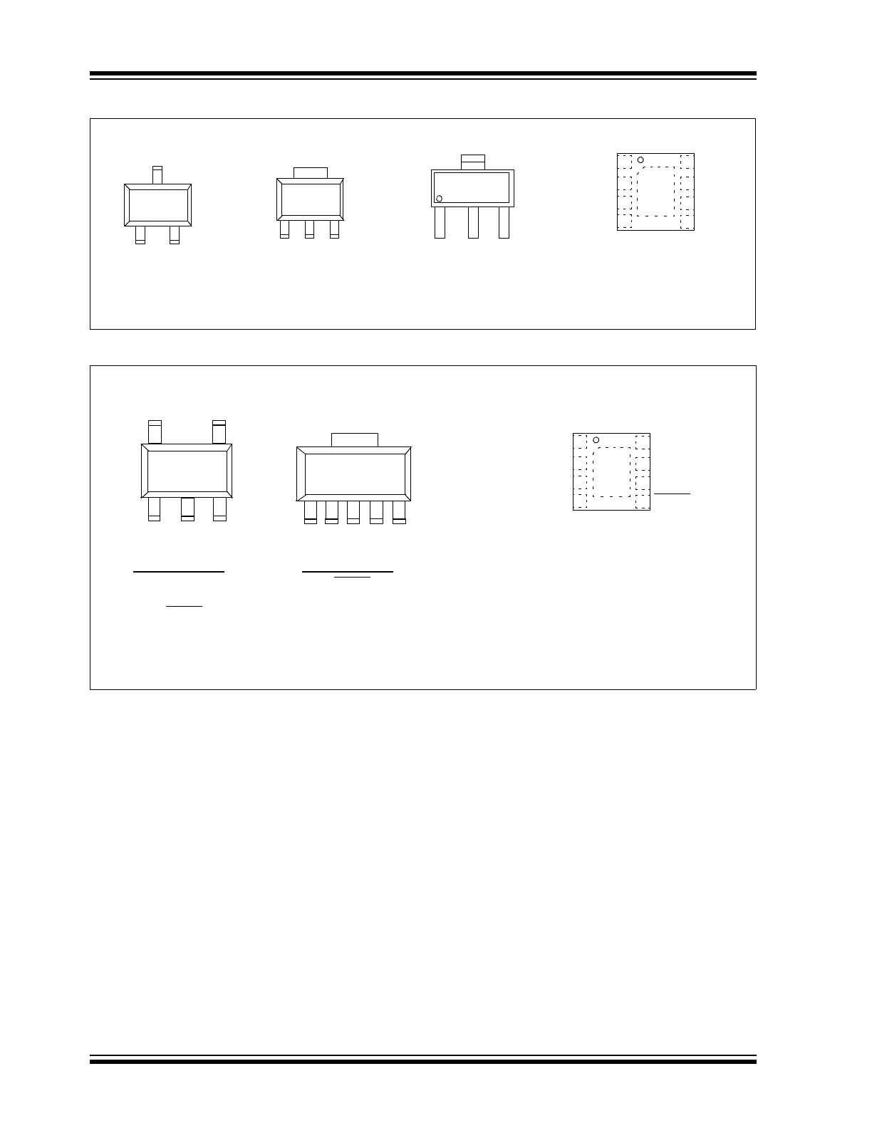
Package Types – MCP1754S
Package Types – MCP1754
1
3
2
V
IN
GND V
OUT
1
2
3
V
IN
GND V
OUT
3-Pin SOT-23A
3-Pin SOT-89
GND
Tab is connected to GND
8-Lead 2X3 DFN(*)
1
2
3
SOT-223-3
4
GND
V
IN
V
OUT
GND
2
NC
NC
GND
NC
NC
1
2
3
4
8
7
6
5 NC
V
IN
V
OUT
EP
9
* Includes Exposed Thermal Pad (EP); see
Table 3-2
.
(Note: The 3-lead SOT-223 (DB) is
not a standard package for output
voltages below 3.0V)
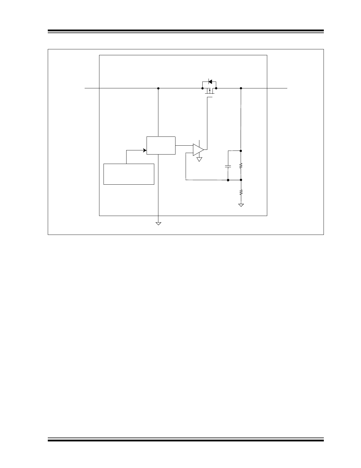
1
2
SOT23-5
1
2
3
SOT-223-5
4
5
PIN FUNCTION
1 SHDN
5 PWRGD
3 GND
4 V
OUT
2 V
IN
4
3
5
PIN FUNCTION
4 PWRGD
2 GND
1 V
IN
5 V
OUT
3 SHDN
Tab is connected to GND
8-Lead 2X3 DFN(*)
3
NC
PWRGD
GND
NC
NC
1
2
3
4
8
7
6
5 SHDN
V
IN
V
OUT
EP
9
* Includes Exposed Thermal Pad (EP); see
Table 3-1
.
2011-2013 Microchip Technology Inc.
DS20002276C-page 3
MCP1754/MCP1754S
Functional Block Diagram – MCP1754S
+
-
MCP1754S
V
IN
V
OUT
GND
+V
IN
Error Amplifier
Voltage
Reference
Overcurrent
Overtemperature
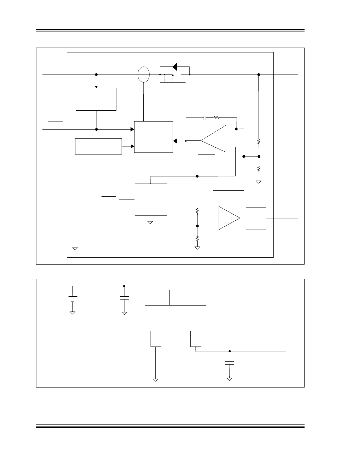
MCP1754/MCP1754S
DS20002276C-page 4
2011-2013 Microchip Technology Inc.
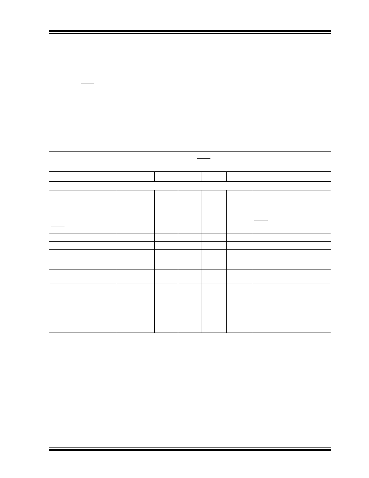
Functional Block Diagram – MCP1754
Typical Application Circuits
EA
+
–
V
OUT
PMOS
R
f
C
f
I
SNS
Overtemperature
V
REF
Comp
92% of V
REF
T
DELAY
V
IN
Driver w/limit
and SHDN
GND
Soft-Start
Sense
Undervoltage
Lock Out
VIN
Reference
SHDN
SHDN
SHDN
Sensing
(UVLO)
PWRGD
MCP1754
MCP1754S
C
IN
1 µF Ceramic
C
OUT
1 µF Ceramic
V
OUT
5.0V
I
OUT
30 mA
V
IN
V
OU
T
12V
+
GN
D
2011-2013 Microchip Technology Inc.
DS20002276C-page 5
MCP1754/MCP1754S
1.0
ELECTRICAL
CHARACTERISTICS
Absolute Maximum Ratings †
Input Voltage, V
IN
..................................................................+
17.6V
VIN, PWRGD, SHDN ..................... (GND-0.3V) to (V
IN
+0.3V)
VOUT .................................................. (GND-0.3V) to (+5.5V)
Internal Power Dissipation ............ Internally-Limited (
Note 6
)
Output Short Circuit Current ................................. Continuous
Storage temperature .....................................-55°C to +150°C
Maximum Junction Temperature .....................165°C (
Note 7
)
Operating Junction Temperature...................-40°C to +150°C
ESD protection on all pins
kV HBM and 200V MM
† Notice: Stresses above those listed under “Maximum
Ratings” may cause permanent damage to the device. This is
a stress rating only and functional operation of the device at
those or any other conditions above those indicated in the
operational listings of this specification is not implied.
Exposure to maximum rating conditions for extended periods
may affect device reliability.
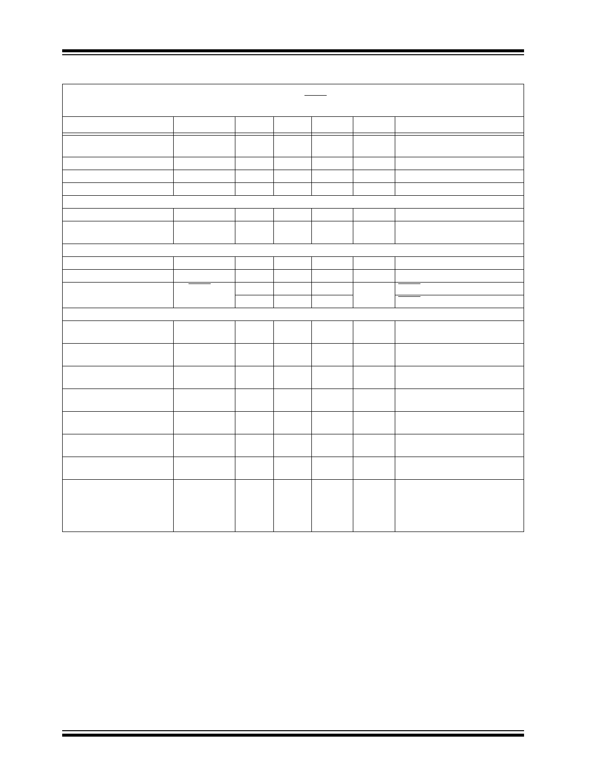
AC/DC CHARACTERISTICS
Electrical Specifications: Unless otherwise specified, all limits are established for V
IN
= V
R
+ 1V,
Note 1
, I
LOAD
= 1 mA,
C
OUT
= 1 µF (X7R), C
IN
= 1 µF (X7R), T
A
= +25°C, t
r(VIN)
= 0.5V/µs, SHDN = V
IN
, PWRGD = 10K to V
OUT
.
Boldface type applies for junction temperatures, T
J
(
Note 7
) of -40°C to +125°C.
Parameters
Sym.
Min.
Typ.
Max.
Units
Conditions
Input/Output Characteristics
Input Operating Voltage
V
IN
3.6
—
16.0
V
Output Voltage Operating
Range
V
OUT-RANGE
1.8
—
5.5
V
Input Quiescent Current
I
q
—
56
90
µA
I
L
= 0 mA
Input Quiescent Current for
SHDN mode
I
SHDN
—
0.1
5
µA
SHDN = GND
Ground Current
I
GND
—
150
250
µA
I
LOAD
= 150 mA
Maximum Output Current
I
OUT
150
—
—
mA
Output Soft Current
Limit
I
OUT_SCL
—
250
—
mA
V
IN
= V
IN(MIN)
, V
OUT
0.1V,
Current measured 10 ms after load
is applied
Output Pulse Current
Limit
I
OUT_PCL
—
250
—
mA
Pulse Duration < 100 ms, Duty
Cycle < 50%, V
OUT
0.1V,
Note 6
Output Short Circuit
Foldback Current
I
OUT_SC
—
30
—
mA
V
IN
= V
IN(MIN)
, V
OUT
= GND
Output Voltage Overshoot on
Startup
V
OVER
—
0.5
—
%V
OUT
V
IN
= 0 to 16V, I
LOAD
= 150 mA
Output Voltage Regulation
V
OUT
V
R
-2.0%
V
R
±0.2%
V
R
+2.0%
V
Note 2
V
OUT
Temperature
Coefficient
TCV
OUT
—
22
ppm/°C
Note 3
Note
1:
The minimum V
IN
must meet two conditions: V
IN
3.6V and V
IN
V
R
+ V
DROPOUT(MAX)
.
2:
V
R
is the nominal regulator output voltage when the input voltage V
IN
= V
Rated
+ V
DROPOUT(MAX)
or V
IN
= 3.6V
(whichever is greater); I
OUT
= 1 mA.
3:
TCV
OUT
= (V
OUT-HIGH
– V
OUT-LOW
) *10
6
/(V
R
*
Temperature), V
OUT-HIGH
= highest voltage measured over the
temperature range. V
OUT-LOW
= lowest voltage measured over the temperature range.
4:
Load regulation is measured at a constant junction temperature using low duty cycle pulse testing. Changes in output
voltage due to heating effects are determined using thermal regulation specification TCV
OUT
.
5:
Dropout voltage is defined as the input to output differential at which the output voltage drops 2% below the output
voltage value that was measured with an applied input voltage of V
IN
= V
R
+ 1V or V
IN
= 3.6V (whichever is greater).
6:
The maximum allowable power dissipation is a function of ambient temperature, the maximum allowable junction
temperature and the thermal resistance from junction to air (i.e., T
A
, T
J
,
JA
). Exceeding the maximum allowable power
dissipation causes the device operating junction temperature to exceed the maximum 150°C rating. Sustained junction
temperatures above +150°C can impact the device reliability.
7:
The junction temperature is approximated by soaking the device under test at an ambient temperature equal to the
desired junction temperature. The test time is small enough such that the rise in the junction temperature over the
ambient temperature is not significant.
MCP1754/MCP1754S
DS20002276C-page 6
2011-2013 Microchip Technology Inc.
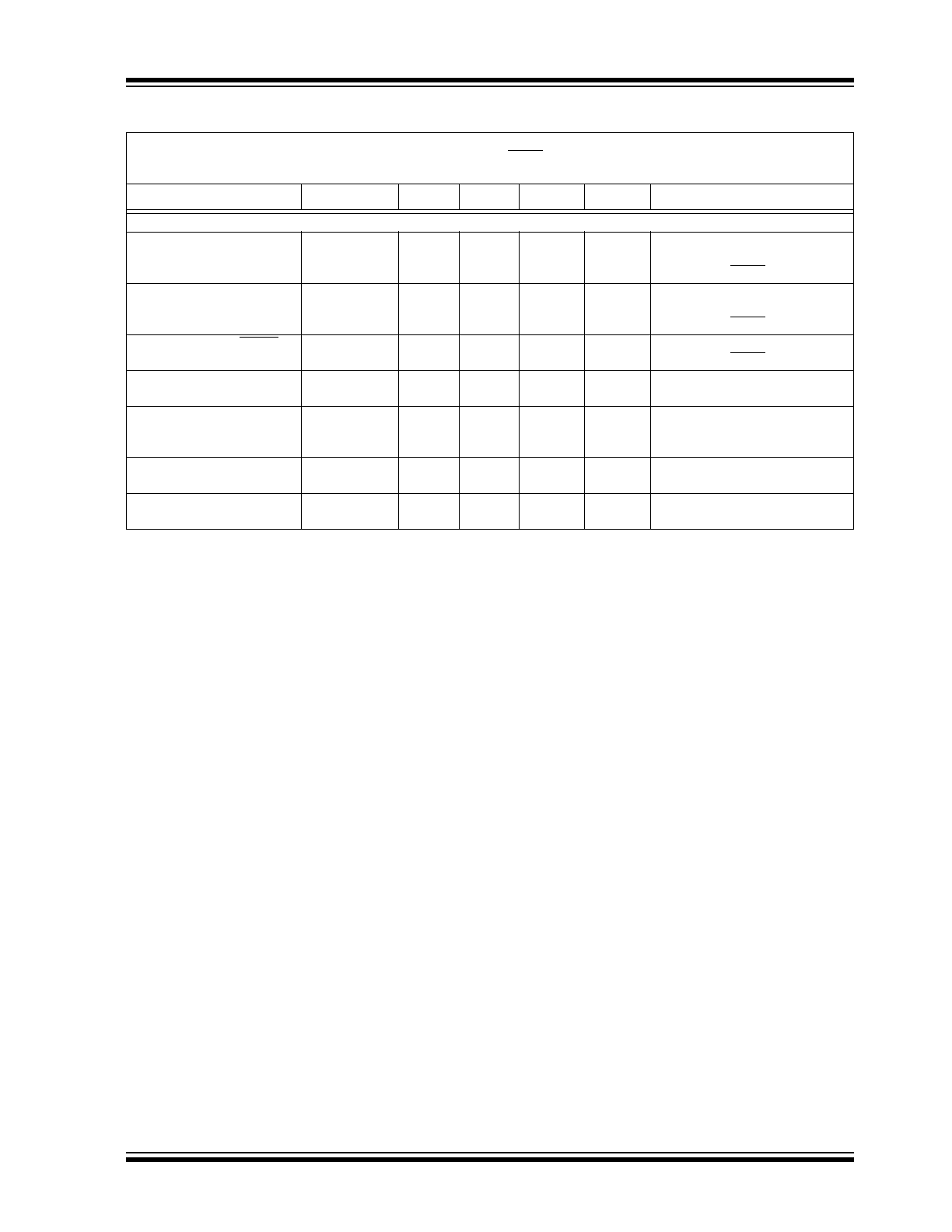
Line Regulation
V
OUT
/
(V
OUT
x
V
IN
)
-0.05
±0.01
+0.05
%/V
V
R
+ 1V
V
IN
16V
Load Regulation
V
OUT
/V
OUT
-1.1
-0.4
0
%
I
L
= 1.0 mA to 150 mA,
Note 4
Dropout Voltage (
Note 5
)
V
DROPOUT
—
300
500
mV
I
L
= 150 mA
Dropout Current
I
DO
—
50
85
µA
V
IN
= 0.95V
R
, I
OUT
= 0 mA
Undervoltage Lockout
Undervoltage Lockout
UVLO
—
2.95
—
V
Rising V
IN
Undervoltage Lockout
Hysteresis
UVLO
HYS
—
285
—
mV
Falling V
IN
Shutdown Input
Logic High Input
V
SHDN-HIGH
2.4
—
V
IN(MAX)
V
Logic Low Input
V
SHDN-LOW
0.0
—
0.8
V
Shutdown Input Leakage
Current
SHDN
ILK
—
0.100
0.500
µA
SHDN = GND
—
0.500
2.0
SHDN = 16V
Power Good Output
PWRGD Input Voltage
Operating Range
V
PWRGD_VIN
1.7
—
V
IN
V
I
SINK
= 1 mA
PWRGD Threshold Voltage
(Referenced to V
OUT
)
V
PWRGD_TH
90
92
94
%V
OUT
Falling Edge of V
OUT
PWRGD Threshold
Hysteresis
V
PWRGD_HYS
—
2.0
—
%V
OUT
Rising Edge of V
OUT
PWRGD Output Voltage Low
V
PWRGD_L
—
0.2
0.6
V
I
PWRGD_SINK
= 5.0 mA,
V
OUT
= 0V
PWRGD Output Sink
Current
I
PWRGD_L
5.0
—
—
mA
V
PWRGD
0.4V
PWRGD Leakage Current
I
PWRGD_LK
—
40
700
nA
V
PWRGD
Pullup = 10 k
to V
IN,
V
IN
= 16V
PWRGD Time Delay
T
PG
—
100
—
µs
Rising Edge of V
OUT
,
R
PULLUP
= 10 k
Detect Threshold to PWRGD
Active Time Delay
T
VDET_PWRGD
—
200
—
µs
Falling Edge of V
OUT
after
Transition from
V
OUT
= V
PRWRGD_TH
+ 50 mV, to
V
PWRGD_TH
- 50 mV,
R
PULLUP
= 10k
to V
IN
AC/DC CHARACTERISTICS (CONTINUED)
Electrical Specifications: Unless otherwise specified, all limits are established for V
IN
= V
R
+ 1V,
Note 1
, I
LOAD
= 1 mA,
C
OUT
= 1 µF (X7R), C
IN
= 1 µF (X7R), T
A
= +25°C, t
r(VIN)
= 0.5V/µs, SHDN = V
IN
, PWRGD = 10K to V
OUT
.
Boldface type applies for junction temperatures, T
J
(
Note 7
) of -40°C to +125°C.
Parameters
Sym.
Min.
Typ.
Max.
Units
Conditions
Note
1:
The minimum V
IN
must meet two conditions: V
IN
3.6V and V
IN
V
R
+ V
DROPOUT(MAX)
.
2:
V
R
is the nominal regulator output voltage when the input voltage V
IN
= V
Rated
+ V
DROPOUT(MAX)
or V
IN
= 3.6V
(whichever is greater); I
OUT
= 1 mA.
3:
TCV
OUT
= (V
OUT-HIGH
– V
OUT-LOW
) *10
6
/(V
R
*
Temperature), V
OUT-HIGH
= highest voltage measured over the
temperature range. V
OUT-LOW
= lowest voltage measured over the temperature range.
4:
Load regulation is measured at a constant junction temperature using low duty cycle pulse testing. Changes in output
voltage due to heating effects are determined using thermal regulation specification TCV
OUT
.
5:
Dropout voltage is defined as the input to output differential at which the output voltage drops 2% below the output
voltage value that was measured with an applied input voltage of V
IN
= V
R
+ 1V or V
IN
= 3.6V (whichever is greater).
6:
The maximum allowable power dissipation is a function of ambient temperature, the maximum allowable junction
temperature and the thermal resistance from junction to air (i.e., T
A
, T
J
,
JA
). Exceeding the maximum allowable power
dissipation causes the device operating junction temperature to exceed the maximum 150°C rating. Sustained junction
temperatures above +150°C can impact the device reliability.
7:
The junction temperature is approximated by soaking the device under test at an ambient temperature equal to the
desired junction temperature. The test time is small enough such that the rise in the junction temperature over the
ambient temperature is not significant.
2011-2013 Microchip Technology Inc.
DS20002276C-page 7
MCP1754/MCP1754S
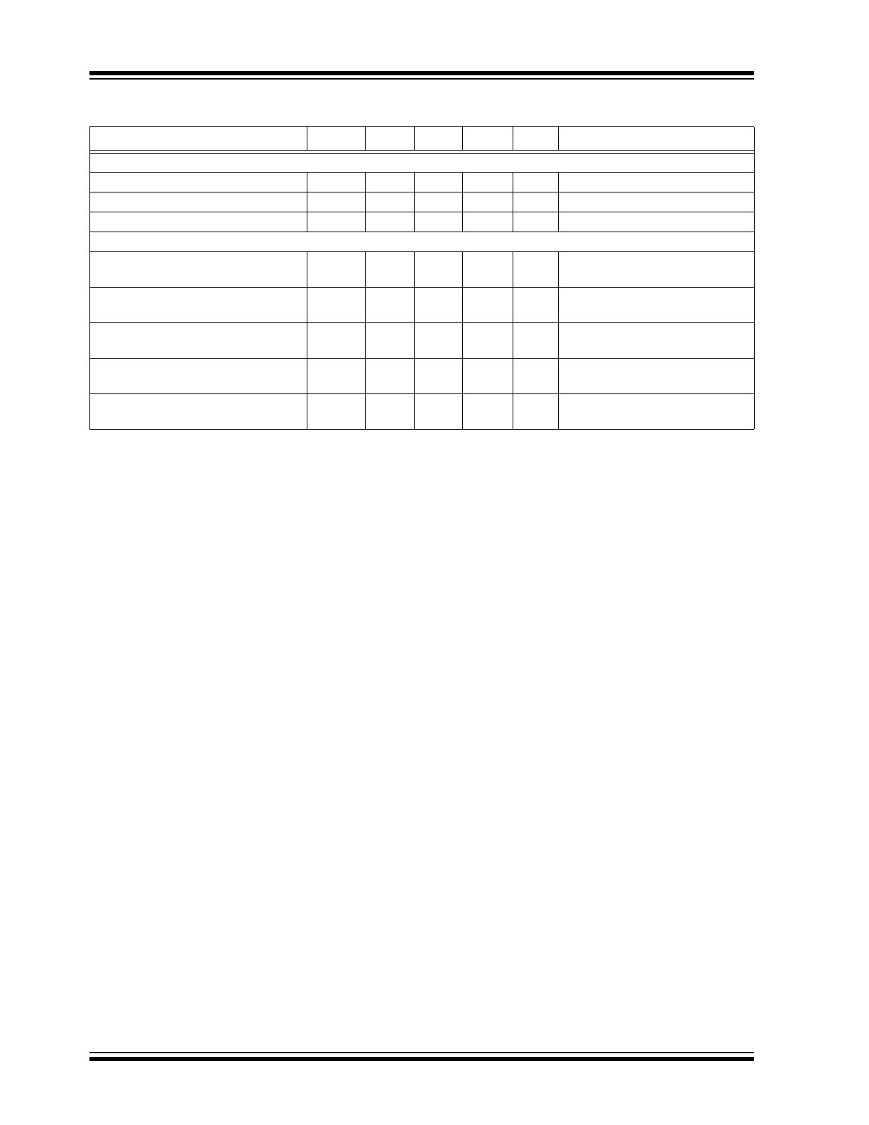
AC Performance
Output Delay From V
IN
To
V
OUT
= 90% V
REG
T
DELAY
—
240
—
µs
V
IN
= 0V to 16V, V
OUT
= 90% V
R
,
t
r
(VIN)
= 5V/µs,
C
OUT
= 1 µF, SHDN = V
IN
Output Delay From V
IN
To
V
OUT
> 0.1V
T
DELAY_START
—
80
—
µs
V
IN
= 0V to 16V, V
OUT
0.1V,
t
r
(VIN)
= 5V/µs,
C
OUT
= 1 µF, SHDN = V
IN
Output Delay From SHDN
to V
OUT
= 90% V
REG
T
DELAY_SHDN
—
160
—
µs
V
IN
= 16V, V
OUT
= 90% V
R
,
C
OUT
= 1 µF, SHDN = GND to V
IN
Output Noise
e
N
—
3
—
µV/(Hz)
1/2
I
L
= 50 mA, f = 1 kHz,
C
OUT
= 1 µF
Power Supply Ripple
Rejection Ratio
PSRR
—
72
—
dB
V
R
= 5V, f = 1 kHz, I
L
= 150 mA,
V
INAC
= 1V pk-pk, C
IN
= 0 µF,
V
IN
= V
R
+ 1.5V
Thermal Shutdown
Temperature
T
SD
—
150
—
°C
Note 6
Thermal Shutdown
Hysteresis
TSD
—
10
—
°C
AC/DC CHARACTERISTICS (CONTINUED)
Electrical Specifications: Unless otherwise specified, all limits are established for V
IN
= V
R
+ 1V,
Note 1
, I
LOAD
= 1 mA,
C
OUT
= 1 µF (X7R), C
IN
= 1 µF (X7R), T
A
= +25°C, t
r(VIN)
= 0.5V/µs, SHDN = V
IN
, PWRGD = 10K to V
OUT
.
Boldface type applies for junction temperatures, T
J
(
Note 7
) of -40°C to +125°C.
Parameters
Sym.
Min.
Typ.
Max.
Units
Conditions
Note
1:
The minimum V
IN
must meet two conditions: V
IN
3.6V and V
IN
V
R
+ V
DROPOUT(MAX)
.
2:
V
R
is the nominal regulator output voltage when the input voltage V
IN
= V
Rated
+ V
DROPOUT(MAX)
or V
IN
= 3.6V
(whichever is greater); I
OUT
= 1 mA.
3:
TCV
OUT
= (V
OUT-HIGH
– V
OUT-LOW
) *10
6
/(V
R
*
Temperature), V
OUT-HIGH
= highest voltage measured over the
temperature range. V
OUT-LOW
= lowest voltage measured over the temperature range.
4:
Load regulation is measured at a constant junction temperature using low duty cycle pulse testing. Changes in output
voltage due to heating effects are determined using thermal regulation specification TCV
OUT
.
5:
Dropout voltage is defined as the input to output differential at which the output voltage drops 2% below the output
voltage value that was measured with an applied input voltage of V
IN
= V
R
+ 1V or V
IN
= 3.6V (whichever is greater).
6:
The maximum allowable power dissipation is a function of ambient temperature, the maximum allowable junction
temperature and the thermal resistance from junction to air (i.e., T
A
, T
J
,
JA
). Exceeding the maximum allowable power
dissipation causes the device operating junction temperature to exceed the maximum 150°C rating. Sustained junction
temperatures above +150°C can impact the device reliability.
7:
The junction temperature is approximated by soaking the device under test at an ambient temperature equal to the
desired junction temperature. The test time is small enough such that the rise in the junction temperature over the
ambient temperature is not significant.
MCP1754/MCP1754S
DS20002276C-page 8
2011-2013 Microchip Technology Inc.
TEMPERATURE SPECIFICATIONS (
Note 1
)
Parameters
Sym.
Min.
Typ.
Max.
Units
Conditions
Temperature Ranges
Specified Temperature Range
T
A
-40
+125
°C
Operating Temperature Range
T
J
-40
+150
°C
Storage Temperature Range
T
A
-55
+150
°C
Thermal Package Resistance
Thermal Resistance, SOT-223-3
JA
JC
—
—
62
15
—
—
°C/W
Thermal Resistance, SOT-23A-3
JA
JC
—
—
336
110
—
—
°C/W
Thermal Resistance, SOT-89-3
JA
JC
—
—
153.3
100
—
—
°C/W
Thermal Resistance, SOT-223-5
JA
JC
—
—
62
15
—
—
°C/W
Thermal Resistance, 2X3 DFN
JA
JC
—
—
93
26
—
—
°C/W
Note 1:
The maximum allowable power dissipation is a function of ambient temperature, the maximum allowable
junction temperature and the thermal resistance from junction to air (i.e., T
A
, T
J
,
JA
). Exceeding the
maximum allowable power dissipation causes the device operating junction temperature to exceed the
maximum +150°C rating. Sustained junction temperatures above +150°C can impact the device reliability.
2011-2013 Microchip Technology Inc.
DS20002276C-page 9
MCP1754/MCP1754S
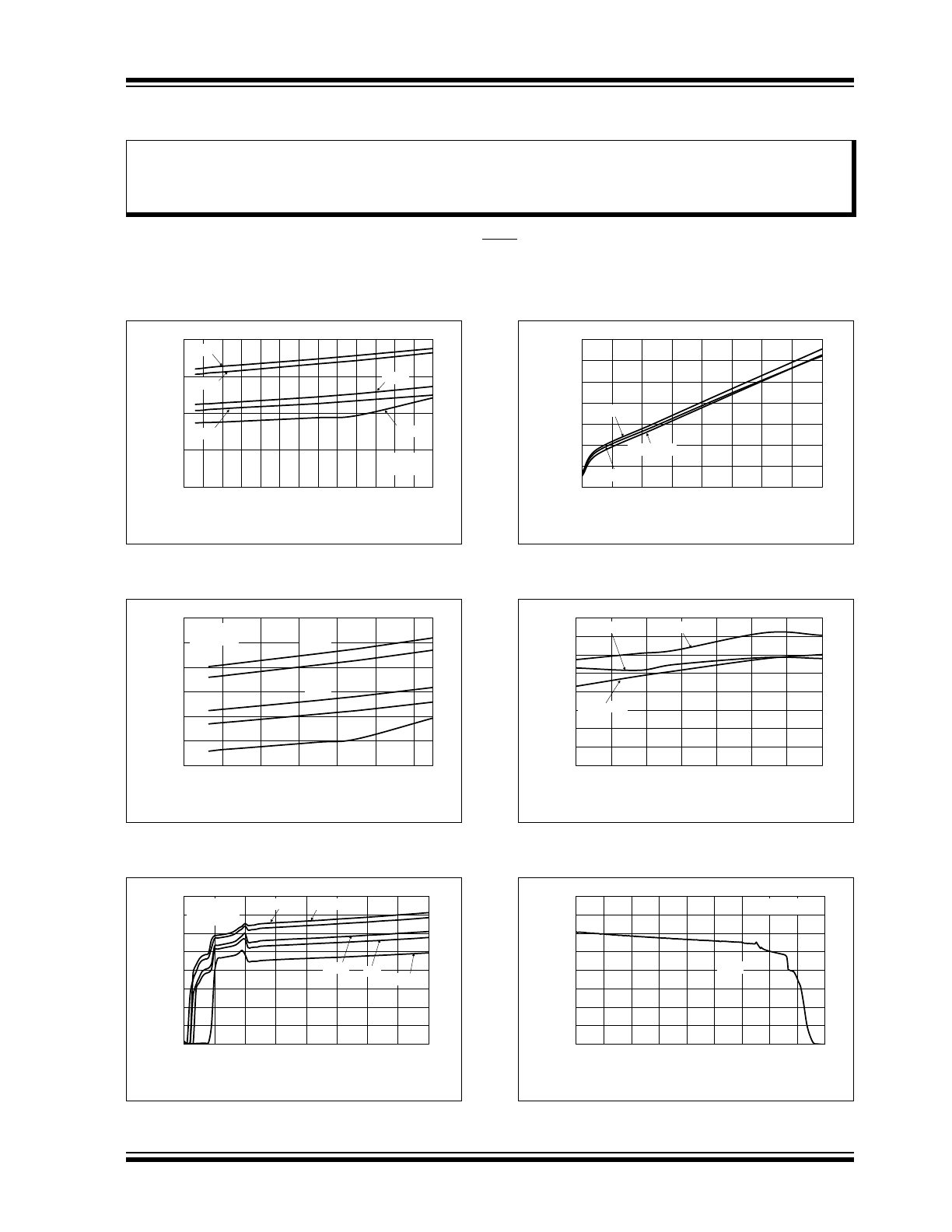
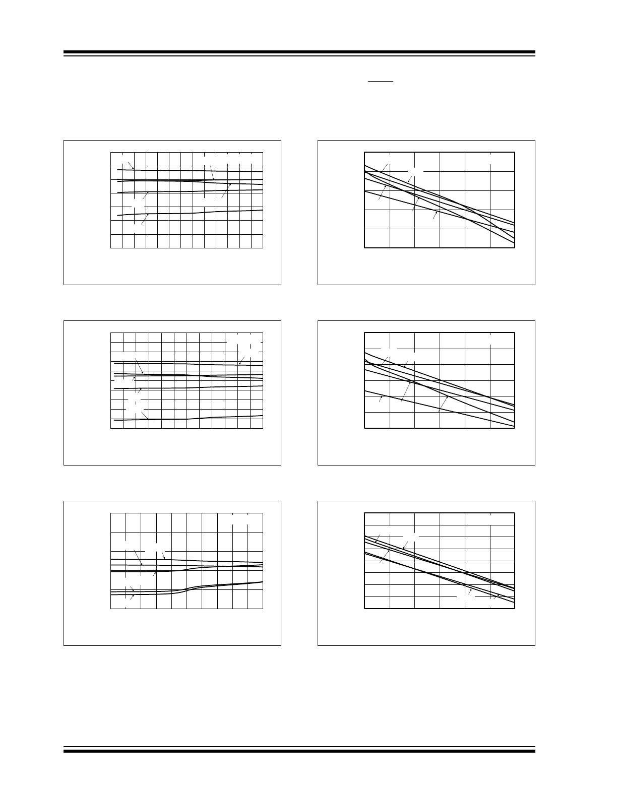
2.0
TYPICAL PERFORMANCE CURVES
Note 1:
Unless otherwise indicated
V
R
= 3.3V, C
OUT
= 1 µF Ceramic (X7R), C
IN
= 1 µF Ceramic (X7R), I
L
= 1 mA, T
A
= +25°C,
V
IN
= V
R
+ 1V or V
IN
= 3.6V (whichever is greater), SHDN = V
IN
, package = SOT-223.
2:
Junction Temperature (T
J
) is approximated by soaking the device under test to an ambient temperature equal to the
desired junction temperature. The test time is small enough such that the rise in junction temperature over the ambient
temperature is not significant.
FIGURE 2-1:
Quiescent Current vs. Input
Voltage.
FIGURE 2-2:
Quiescent Current vs. Input
Voltage.
FIGURE 2-3:
Quiescent Current vs. Input
Voltage.
FIGURE 2-4:
Ground Current vs. Load
Current.
FIGURE 2-5:
Quiescent Current vs.
Junction Temperature.
FIGURE 2-6:
Quiescent Current vs. Input
Voltage.
Note:
The graphs and tables provided following this note are a statistical summary based on a limited number of
samples and are provided for informational purposes only. The performance characteristics listed herein
are not tested or guaranteed. In some graphs or tables, the data presented may be outside the specified
operating range (e.g., outside specified power supply range) and therefore outside the warranted range.
40
50
60
70
80
3
4
5
6
7
8
9
10 11 12 13 14 15 16
Quiescent Current (µA)
Input Voltage (V)
V
OUT
= 1.8V
I
OUT
= 0 µA
+25°C
+130°C
-45°C
0°C
+90°C
40
45
50
55
60
65
70
3
5
7
9
11
13
15
Quiescent Current (µA)
Input Voltage (V)
V
OUT
= 3.3V
I
OUT
= 0 µA
+25°C
+130°C
-45°C
0°C
+90°C
0
10
20
30
40
50
60
70
80
1.0
3.0
5.0
7.0
9.0
11.0 13.0 15.0 17.0
Quiescent Current (µA)
Input Voltage (V)
V
OUT
= 5.0V
I
OUT
= 0 µA
+25°C
+130°C
-45°C
0°C
+90°C
40
60
80
100
120
140
160
180
0
20
40
60
80
100
120
140
160
GND Current (µA)
Load Current (mA)
V
OUT
= 5.0V
V
OUT
= 3.3V
V
OUT
= 1.8V
0
10
20
30
40
50
60
70
80
-45
-20
5
30
55
80
105
130
Quiescent Current (µA)
Junction Temperature (°C)
V
OUT
= 5.0V
V
OUT
= 1.8V
V
OUT
= 3.3V
0
10
20
30
40
50
60
70
80
0
2
4
6
8
10
12
14
16
18
Quiescent Current (µA)
Input Voltage (V)
V
OUT
= 5.0V
+25°C
MCP1754/MCP1754S
DS20002276C-page 10
2011-2013 Microchip Technology Inc.
Note 1: Unless otherwise indicated
V
R
= 3.3V, C
OUT
= 1 µF Ceramic (X7R), C
IN
= 1 µF Ceramic (X7R), I
L
= 1 mA,
T
A
= +25°C, V
IN
= V
R
+ 1V or V
IN
= 3.6V (whichever is greater), SHDN = V
IN
, package = SOT-223.
2: Junction Temperature (T
J
) is approximated by soaking the device under test to an ambient temperature
equal to the desired junction temperature. The test time is small enough such that the rise in junction
temperature over the ambient temperature is not significant.
FIGURE 2-7:
Output Voltage vs. Input
Voltage.
FIGURE 2-8:
Output Voltage vs. Input
Voltage.
FIGURE 2-9:
Output Voltage vs. Input
Voltage.
FIGURE 2-10:
Output Voltage vs. Load
Current.
FIGURE 2-11:
Output Voltage vs. Load
Current.
FIGURE 2-12:
Output Voltage vs. Load
Current.
1.800
1.802
1.804
1.806
1.808
1.810
1.812
1.814
3
4
5
6
7
8
9 10 11 12 13 14 15 16
Output V
o
ltage
(V)
Input Voltage (V)
V
OUT
= 1.8V
+25°C
+130°C
-45°C
0°C
+90°C
3.290
3.292
3.294
3.296
3.298
3.300
3.302
3.304
3.306
3.308
3.310
4
5
6
7
8
9
10 11 12 13 14 15 16
Output V
o
ltage
(V)
Input Voltage (V)
V
OUT
= 3.3V
+25°C
+130°C
-45°C
0°C
+90°C
5.000
5.004
5.008
5.012
5.016
5.020
6
7
8
9
10
11
12
13
14
15
16
Output V
o
ltage
(V)
Input Voltage (V)
V
OUT
= 5.0V
+25°C
+130°C
-45°C
0°C
+90°C
1.790
1.795
1.800
1.805
1.810
1.815
0
25
50
75
100
125
150
Output V
o
ltage
(V)
Load Current (mA)
V
OUT
= 1.8V
25°C
90°C
130°C
0°C
-45°C
3.280
3.285
3.290
3.295
3.300
3.305
3.310
0
25
50
75
100
125
150
Output V
o
ltage
(V)
Load Current (mA)
V
OUT
= 3.3V
25°C
90°C
0°C
-45°C
130°C
4.980
4.985
4.990
4.995
5.000
5.005
5.010
5.015
5.020
0
25
50
75
100
125
150
Output V
o
ltage
(V)
Load Current (mA)
V
OUT
= 5.0V
25°C
90°C
0°C
-45°C
130°C