
2015-2016 Microchip Technology Inc.
DS20005415D-page 1
MCP1711
Features
• Low Quiescent Current: 600 nA
• Input Voltage Range: 1.4V to 6.0V
• Standard Output Voltages: 1.2V, 1.8V, 1.9V, 2.0V,
2.2V, 2.5V, 3.0V, 3.3V, 5.0V
• Output Accuracy: ±20 mV for 1.2V and 1.8V
Options and ±1% for V
R
2.0V
• Temperature Stability: ±50 ppm/°C
• Maximum Output Current: 150 mA
• Low ON Resistance: 3.3
@ V
R
= 3.0V
• Standby Current: 10 nA
• Protection Circuits: Current Limiter, Short Circuit,
Foldback
• SHDN Pin Function: ON/OFF Logic = Enable
High
• C
OUT
Discharge Circuit when SHDN Function is
Active
• Output Capacitor: Low Equivalent Series
Resistance (ESR) Ceramic, Capacitorless
Compatible
• Operating Temperature: -40°C to +85°C
(Industrial)
• Available Packages:
- 4-Lead 1 x 1 mm UQFN
- 5-Lead SOT-23
• Environmentally Friendly: EU RoHS Compliant,
Lead-Free
Applications
• Energy Harvesting
• Long-Life, Battery-Powered Applications
• Portable Electronics
• Ultra-Low Consumption “Green” Products
• Mobile Devices/Terminals
• Wireless LAN
• Modules (Wireless, Cameras)
Related Literature
• AN765, Using Microchip’s Micropower LDOs
(DS00765), Microchip Technology Inc.
• AN766, Pin-Compatible CMOS Upgrades to Bipolar
LDOs (DS00766), Microchip Technology Inc.
• AN792, A Method to Determine How Much Power
a SOT23 Can Dissipate in an Application
(DS00792), Microchip Technology Inc.
General Description
The MCP1711 is a highly accurate CMOS low dropout
(LDO) voltage regulator that can deliver up to 150 mA
of current while consuming only 0.6 µA of quiescent
current (typical). The input operating range is specified
from 1.4V to 6.0V, making it an ideal choice for mobile
applications and one-cell Li-Ion powered applications.
The MCP1711 is capable of delivering 150 mA output
current with only 0.32V (typical) for V
R
= 5.0V, and
1.41V (typical) for V
R
= 1.2V of input-to-output voltages
differential. The output voltage accuracy of the
MCP1711 is typically ± 0.02V for V
R
< 2.0V and ±1% for
V
R
2.0V at +25°C. The temperature stability is
approximately ±50 ppm/°C. Line regulation is
±0.01%/V typical at +25°C.
The output voltages available for the MCP1711 range
from 1.2V to 5.0V. The LDO output is stable even if an
output capacitor is not connected, due to an excellent
internal phase compensation. However, for better tran-
sient responses, the output capacitor should be added.
The MCP1711 is compatible with low ESR ceramic
output capacitors.
Overcurrent limit and short-circuit protection embed-
ded into the device provide a robust solution for any
application.
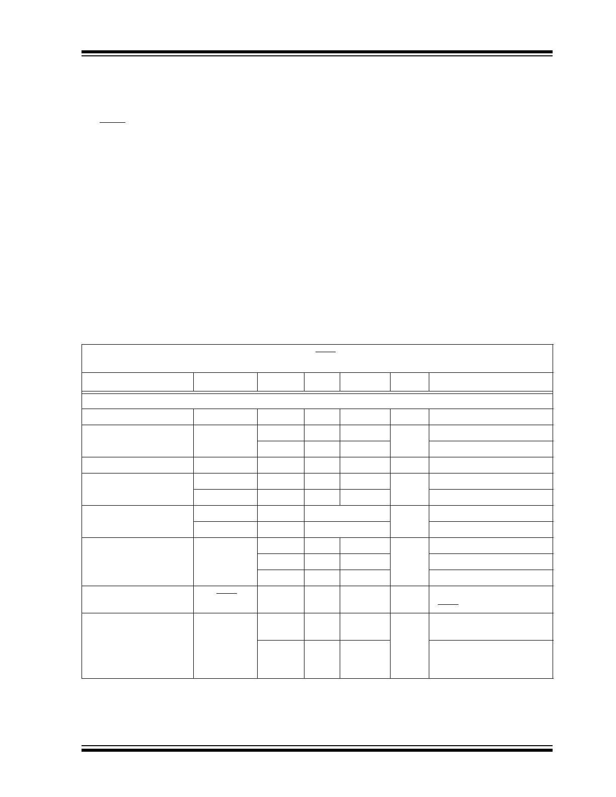
The MCP1711 has a true current foldback feature.
When the load decreases beyond the MCP1711 load
rating, the output current and output voltage will
foldback toward 80 mA (typical) at approximately 0V
output. When the load impedance increases and
returns to the rated load, the MCP1711 will follow the
same foldback curve as the device comes out of
current foldback.
If the device is in Shutdown mode, by inputting a
low-level signal to the SHDN pin, the current
consumption is reduced to less than 0.1 µA (typically
0.01 µA). In Shutdown mode, if the output capacitor is
used, it will be discharged via the internal dedicated
switch and, as a result, the output voltage quickly
returns to 0V.
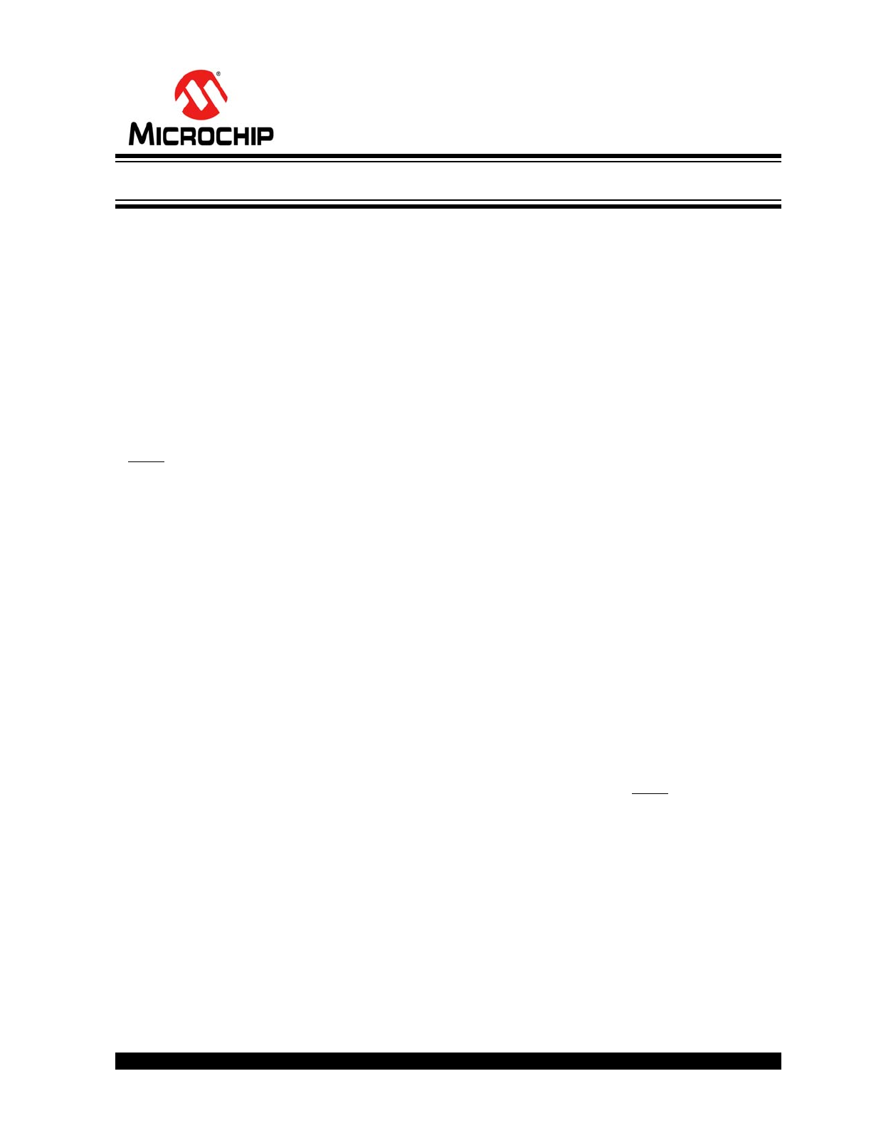
The package options for the MCP1711 are the 4-lead
1 x 1 mm UQFN and the 5-lead SOT-23, which make
the device ideal for small and compact applications.
150 mA Ultra-Low Quiescent Current, Capacitorless LDO Regulator
MCP1711
DS20005415D-page 2
2015-2016 Microchip Technology Inc.
Package Types
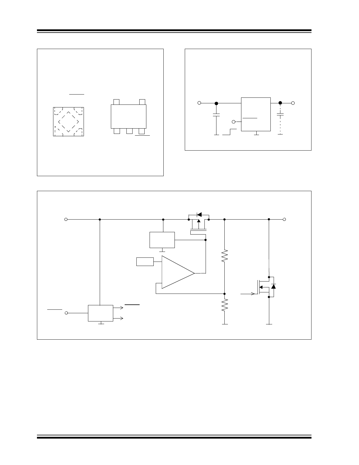
Typical Application Circuit
Functional Block Diagram
2
1
3
4
V
IN
V
OUT
GND
GND
NC
1
2
3
V
OUT
V
IN
SHDN
SHDN
MCP1711
1x1 UQFN*
Top View
EP
5
* Includes Exposed Thermal Pad (EP);
see
Table 3-1
MCP1711
SOT-23
Top View
5
4
V
IN
SHDN
GND
V
OUT
V
IN
C
IN
ON
OFF
C
OUT
V
OUT
MCP1711
0.1 µF
Ceramic
MCP1711
1x1 UQFN and SOT-23
Limit
Ref
–
+
Err Amp
R
1
R
2
Current
SHDN
ON/OFF
Control
V
OUT
V
IN
R
DCHG
SHDN to each block
Discharge transistor (DT)
DT
PMOS
2015-2016 Microchip Technology Inc.
DS20005415D-page 3
MCP1711
1.0
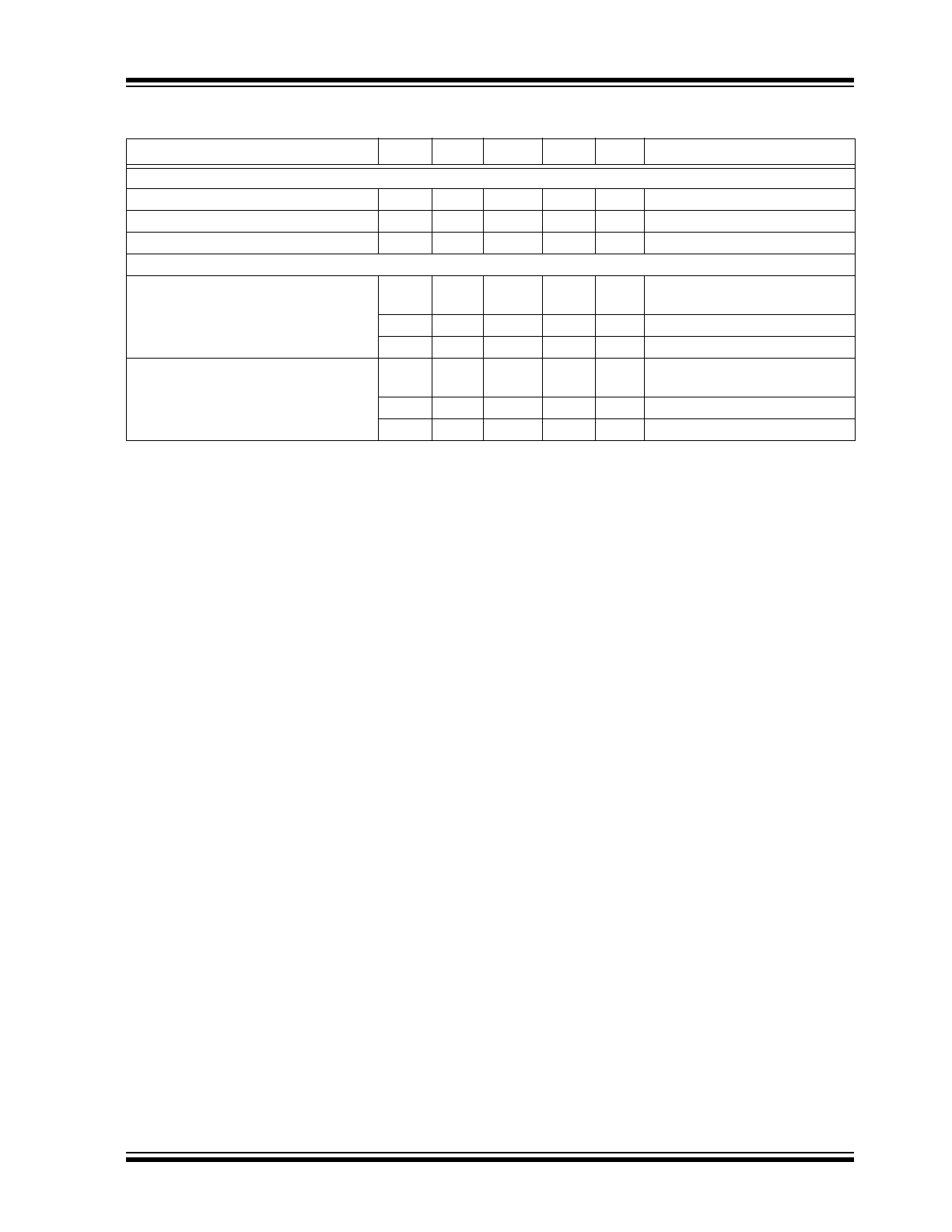
ELECTRICAL CHARACTERISTICS
Absolute Maximum Ratings †
Input Voltage, V
IN
.....................................................................................................................................................+6.5V
V
IN
, SHDN.................................................................................................................................................. -0.3V to +6.5V
Output Current, I
OUT
(
1
)
.........................................................................................................................................470 mA
Output Voltage, V
OUT
(
2
)
....................................................................................................... -0.3V to V
IN
+ 0.3V or +6.5V
Power Dissipation
5-Lead SOT-23 ..................................................... 600 mW (JEDEC 51-7 FR-4 board with thermal vias) or 250 mW
(
3
)
4-Lead 1 x 1 mm UQFN ........................................ 550 mW (JEDEC 51-7 FR-4 board with thermal vias) or 100 mW
(
3
)
Storage Temperature .............................................................................................................................. -55
°
C to +125
°
C
Operating Ambient Temperature ............................................................................................................... -40
°
C to +85
°
C
ESD Protection on all pins ...........................................................................................................±1 kV HBM, ±200V MM
† Notice: Stresses above those listed under “Absolute Maximum Ratings” may cause permanent damage to the device.
This is a stress rating only and functional operation of the device at those or any other conditions above those indicated
in the operational sections of this specification is not intended. Exposure to maximum rating conditions for extended
periods may affect device reliability.
Note 1: Provided that the device is used in the range of I
OUT
P
D
/(V
IN
- V
OUT
).
2: The maximum rating corresponds to the lowest value between V
IN
+ 0.3V or +6.5V.
3: The device is mounted on one layer PCB with minimal copper that does not provide any additional cooling.
DC CHARACTERISTICS
Electrical Characteristics: Unless otherwise indicated, V
SHDN
= V
IN
, I
OUT
= 1 mA, C
IN
= C
OUT
= 0 µF, V
IN
= 3.5V for
V
R
< 2.5V and V
IN
= V
R
+ 1V for V
R
2.5V, T
A
= +25°C
Parameters
Sym.
Min.
Typ.
Max.
Units
Conditions
Input-Output Characteristics
Input Voltage
V
IN
1.4
—
6.0
V
I
OUT
= 1 µA
Output Voltage
V
OUT
V
R
- 0.02
V
R
V
R
+ 0.02
V
V
R
< 2.0V
V
R
x 0.99
V
R
V
R
x 1.01
V
R
2.0V
Maximum Output Current
I
OUT
150
—
—
mA
Load Regulation
V
OUT
-16
±3
+16
mV
1 µA
I
OUT
1 mA
-50
±17
+50
1 mA
I
OUT
150 mA
Dropout Voltage
(
1
)
V
DROPOUT1
—
V
DROP1
(
2
)
V
I
OUT
= 50 mA
V
DROPOUT2
—
V
DROP2
(
2
)
I
OUT
= 150 mA
Input Quiescent Current
I
q
—
0.60
1.27
µA
V
R
< 1.9V
—
0.65
1.50
1.9V
V
R
< 4.0V
—
0.80
1.80
V
R
4.0V
Input Quiescent Current
for SHDN mode
I
SHDN
—
0.01
0.10
µA
V
IN
= 6.0V
V
SHDN
= V
IN
Line Regulation
V
OUT
/
(
V
IN
x V
OUT
)
-0.13
±0.01
+0.13
%/V
I
OUT
= 1 µA
V
R
+ 0.5V
V
IN
6.0V
-0.19
±0.01
+0.19
I
OUT
= 1 mA
VR
1.2V,V
R
+ 0.5V
V
IN
6.0V
Note 1:
The dropout voltage is defined as the input to output differential at which the output voltage drops 2%
below the output voltage value that was measured with an applied input voltage of V
IN
= V
R
+ 1V.
2:
V
DROP1
, V
DROP2
: Dropout Voltage (Refer to the
DC Characteristics Voltage Table
).
MCP1711
DS20005415D-page 4
2015-2016 Microchip Technology Inc.
Output Voltage
Temperature Stability
V
OUT
/
(
T x V
OUT
)
—
±50
—
ppm/°C I
OUT
= 10 mA
-40°C
T
A
+85°C
Current Limit
I
LIMIT
150
270
—
mA
V
OUT
= 0.95 x V
R
Output Short-Circuit
Foldback Current
I
OUT_SC
—
80
—
mA
V
OUT
= GND
C
OUT
Auto-Discharge
Resistance
R
DCHG
280
450
640
SHDN = GND
V
OUT
= V
R
Noise
e
n
—
30
—
µV(rms) C
IN
= C
OUT
= 1 µF, I
OUT
= 50
mA, f = 10 Hz to 100 kHz
Shutdown Input
SHDN Logic High Input
Voltage
V
SHDN-HIGH
0.91
—
6.00
V
SHDN Logic Low Input
Voltage
V
SHDN-LOW
0
—
0.38
V
SHDN High-Level Current
I
SHDN-HIGH
-0.1
—
+0.1
µA
V
IN
= 6.0V
SHDN Low-Level Current
I
SHDN-LOW
-0.1
—
+0.1
µA
V
IN
= 6.0V
SHDN = GND
DC CHARACTERISTICS (CONTINUED)
Electrical Characteristics: Unless otherwise indicated, V
SHDN
= V
IN
, I
OUT
= 1 mA, C
IN
= C
OUT
= 0 µF, V
IN
= 3.5V for
V
R
< 2.5V and V
IN
= V
R
+ 1V for V
R
2.5V, T
A
= +25°C
Parameters
Sym.
Min.
Typ.
Max.
Units
Conditions
Note 1:
The dropout voltage is defined as the input to output differential at which the output voltage drops 2%
below the output voltage value that was measured with an applied input voltage of V
IN
= V
R
+ 1V.
2:
V
DROP1
, V
DROP2
: Dropout Voltage (Refer to the
DC Characteristics Voltage Table
).
DC CHARACTERISTICS VOLTAGE TABLE
Nominal
Output
Voltage
Output Voltage (V)
Dropout Voltage (V)
V
OUT
V
DROP1
V
DROP1
V
DROP2
V
DROP2
V
R
(V)
Min.
Max.
Typ.
Max.
Typ.
Max.
1.2
1.1800
1.2200
0.87
1.23
1.41
1.93
1.8
1.7800
1.8200
0.47
0.72
0.99
1.40
1.9
1.8800
1.9200
0.42
0.64
0.92
1.29
2.0
1.9800
2.0200
0.37
0.58
0.86
1.20
2.2
2.1780
2.2220
0.31
0.47
0.75
1.05
2.5
2.4750
2.5250
0.26
0.40
0.67
0.92
3.0
2.9700
3.0300
0.17
0.26
0.50
0.67
3.3
3.2670
3.3330
0.17
0.26
0.50
0.67
5.0
4.9500
5.0500
0.10
0.16
0.32
0.43
2015-2016 Microchip Technology Inc.
DS20005415D-page 5
MCP1711
TEMPERATURE SPECIFICATIONS
(
Note 1
)
Parameters
Sym.
Min.
Typ.
Max.
Units
Conditions
Temperature Ranges
Operating Ambient Temperature Range
T
A
-40
—
+85
°C
Junction Operating Temperature
T
J
-40
—
+125
°C
Storage Temperature Range
T
A
-55
—
+125
°C
Package Thermal Resistances
Thermal Resistance, 1 x 1 UQFN-4Ld
JA
—
181.82
—
°C/W JEDEC 51-7 FR4 board with
thermal vias
JA
—
1000
—
°C/W
Note 2
JC
—
15
—
°C/W
Thermal Resistance, SOT-23-5Ld
JA
—
166.67
—
°C/W JEDEC 51-7 FR4 board with
thermal vias
JA
—
400
—
°C/W
Note 2
JC
—
81
—
°C/W
Note 1:
The maximum allowable power dissipation is a function of ambient temperature, the maximum allowable
junction temperature, and the thermal resistance from junction to air (i.e., T
A
, T
J
,
JA
). Exceeding the max-
imum allowable power dissipation will cause the device operating junction temperature to exceed the
maximum +125°C rating. Sustained junction temperatures above +125°C can impact the device reliability.
2:
The device is mounted on one layer PCB with minimal copper that does not provide any additional cooling.
MCP1711
DS20005415D-page 6
2015-2016 Microchip Technology Inc.
2.0
TYPICAL PERFORMANCE CURVES
NOTE: Unless otherwise indicated, V
IN
= 3.5V for V
R
< 2.5V or V
IN
= V
R
+ 1V for V
R
2.5V, I
OUT
= 1 mA,
C
IN
= C
OUT
= 0 µF, V
SHDN
= V
IN
, T
A
= +25°C.
FIGURE 2-1:
Quiescent Current vs. Input
Voltage.
FIGURE 2-2:
Quiescent Current vs. Input
Voltage.
FIGURE 2-3:
Quiescent Current vs. Input
Voltage.
FIGURE 2-4:
Quiescent Current vs. Input
Voltage.
FIGURE 2-5:
Ground Current vs. Load
Current.
FIGURE 2-6:
Ground Current vs. Load
Current.
Note:
The graphs and tables provided following this note are a statistical summary based on a limited number of
samples and are provided for informational purposes only. The performance characteristics listed herein
are not tested or guaranteed. In some graphs or tables, the data presented may be outside the specified
operating range (e.g., outside specified power supply range) and therefore outside the warranted range.
0.00
0.20
0.40
0.60
0.80
1.00
1.20
0
1
2
3
4
5
6
Quiescent Current
(µA)
Input Voltage (V)
T
A
= +25°C
T
A
= +85°C
V
R
= 1.2V
T
A
= -40°C
0
0.2
0.4
0.6
0.8
1
1.2
0
1
2
3
4
5
6
Q
u
iescent
Current (
µ
A)
Input Voltage (V)
T
A
= -40°C
T
A
= +25°C
T
A
= +85°C
V
R
= 1.8V
0.00
0.20
0.40
0.60
0.80
1.00
1.20
0
1
2
3
4
5
6
Quiescent Current (µA)
Input Voltage (V)
V
R
= 3.3V
T
A
= -40°C
T
A
= +25°C
T
A
= +85°C
0.00
0.20
0.40
0.60
0.80
1.00
1.20
0
1
2
3
4
5
6
Qu
ie
sc
e
n
t C
u
rr
ent (µ
A)
Input Voltage (V)
T
A
= -40°C
T
A
= +25°C
T
A
= +85°C
V
R
= 5.0V
0
5
10
15
20
25
30
35
40
45
0
30
60
90
120
150
Ground Current (µA)
Load Current (mA)
V
R
= 1.2V
0
5
10
15
20
25
30
35
40
45
0
30
60
90
120
150
Ground Current (µA)
Load Current (mA)
V
R
= 1.8V
2015-2016 Microchip Technology Inc.
DS20005415D-page 7
MCP1711
Note: Unless otherwise indicated, V
IN
= 3.5V for V
R
< 2.5V or V
IN
= V
R
+ 1V for V
R
2.5V, I
OUT
= 1 mA,
C
IN
= C
OUT
= 0 µF, V
SHDN
= V
IN
, T
A
= +25°C.
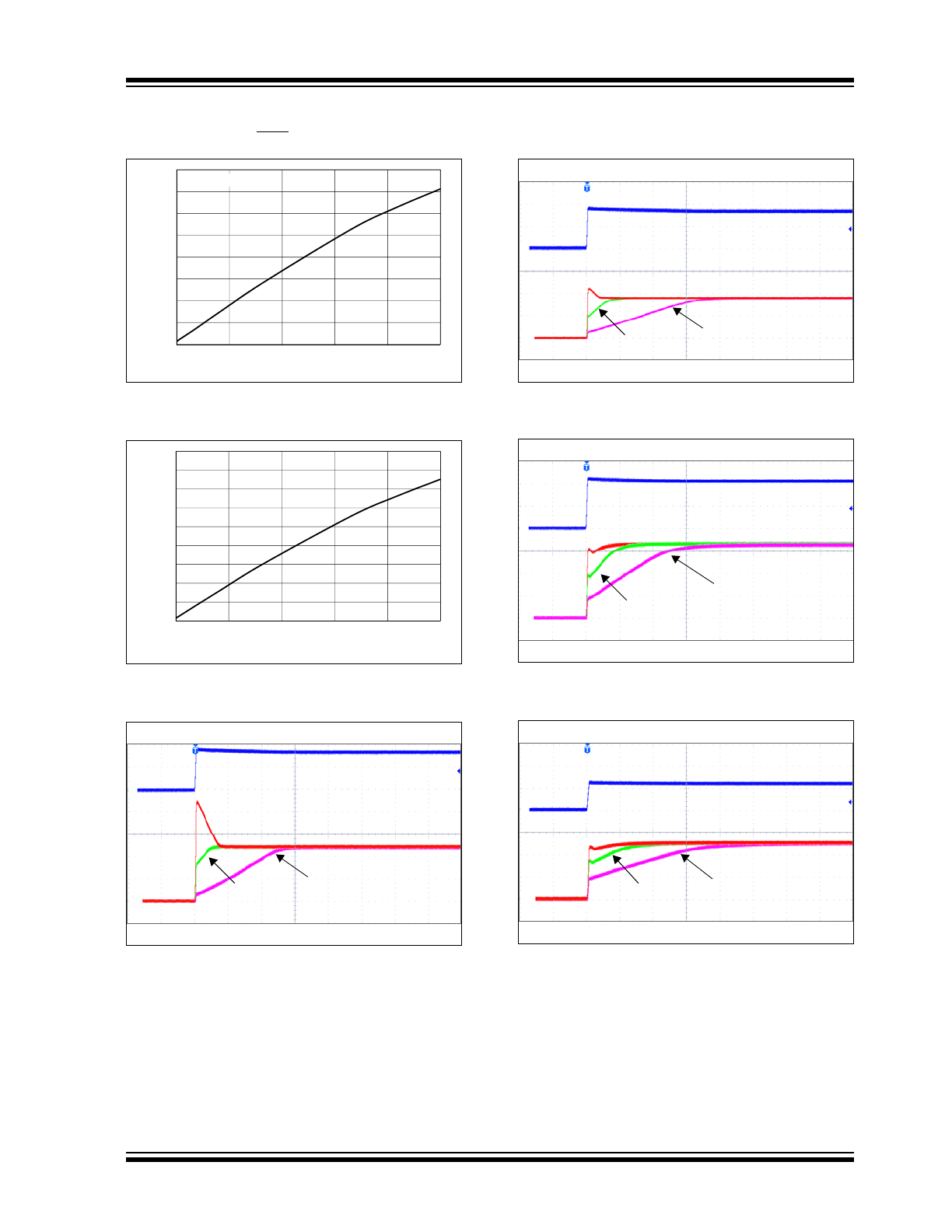
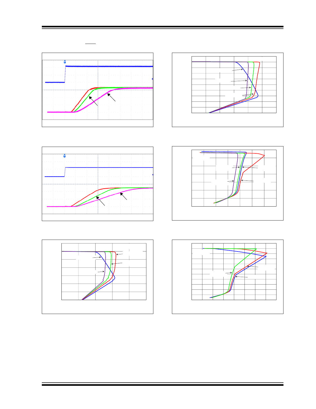
FIGURE 2-7:
Ground Current vs. Load
Current.
FIGURE 2-8:
Ground Current vs. Load
Current.
FIGURE 2-9:
Start-Up from V
IN
.
.
FIGURE 2-10:
Start-Up from V
IN
.
FIGURE 2-11:
Start-Up from V
IN
.
FIGURE 2-12:
Start-Up from V
IN
.
0
5
10
15
20
25
30
35
40
0
30
60
90
120
150
G
round Current
(µA)
Load Current (mA)
V
R
= 3.3V
0
5
10
15
20
25
30
35
40
45
0
30
60
90
120
150
Ground Current (µA)
Load Current (mA)
V
R
= 5.0V
0V
3.5V
t
r
= 5 µs
Time = 80 µs/Div
V
OUT
(DC Coupled, 0.5V/Div)
V
R
= 1.2V
I
OUT
= 1 µA
I
OUT
= 10 mA
I
OUT
= 150 mA
V
IN
V
OUT
0V
3.5V
t
r
= 5 µs
Time = 80 µs/Div
V
OUT
(DC Coupled, 1V/Div)
V
R
= 1.8V
I
OUT
= 1 µA
I
OUT
= 10 mA
I
OUT
= 150 mA
V
IN
V
OUT
0V
4.3V
t
r
= 5 µs
Time = 80 µs/Div
V
OUT
(DC Coupled, 1V/Div)
V
R
= 3.3V
I
OUT
= 1 µA
I
OUT
= 10 mA
I
OUT
= 150 mA
V
IN
V
OUT
0V
6.0 V
t
r
= 5 µs
Time = 80 µs/Div
V
OUT
(DC Coupled, 2V/Div)
V
R
= 5.0V
I
OUT
= 1 µA
I
OUT
= 10 mA
I
OUT
= 150 mA
V
IN
V
OUT
MCP1711
DS20005415D-page 8
2015-2016 Microchip Technology Inc.
Note: Unless otherwise indicated, V
IN
= 3.5V for V
R
< 2.5V or V
IN
= V
R
+ 1V for V
R
2.5V, I
OUT
= 1 mA,
C
IN
= C
OUT
= 0 µF, V
SHDN
= V
IN
, T
A
= +25°C.
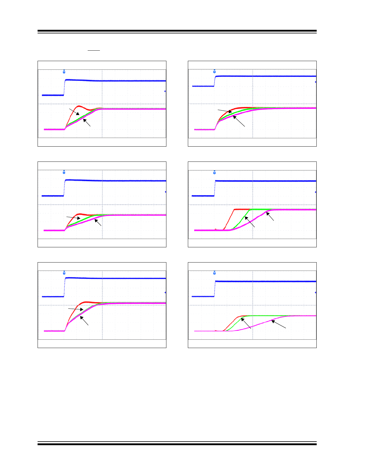
FIGURE 2-13:
Start-Up from V
IN
.
FIGURE 2-14:
Start-Up from V
IN
.
FIGURE 2-15:
Start-Up from V
IN
.
FIGURE 2-16:
Start-Up from V
IN
.
FIGURE 2-17:
Start-Up from SHDN
.
FIGURE 2-18:
Start-Up from SHDN
.
0V
3.5V
t
r
= 5 µs
Time = 80 µs/Div
V
OUT
(DC Coupled, 0.5V/Div)
I
OUT
= 10 mA
I
OUT
= 100 mA
I
OUT
= 150 mA
V
R
= 1.2V
C
IN
= C
OUT
= 1 µF
V
IN
V
OUT
0V
3.5V
t
r
= 5 µs
Time = 80 µs/Div
V
OUT
(DC Coupled, 1V/Div)
I
OUT
= 10 mA
I
OUT
= 100 mA
I
OUT
= 150 mA
V
R
= 1.8V
C
IN
= C
OUT
= 1 µF
V
IN
V
OUT
0V
4.3V
t
r
= 5 µs
Time = 80 µs/Div
V
OUT
(DC Coupled, 1V/Div)
I
OUT
= 10 mA
I
OUT
= 100 mA
I
OUT
= 150 mA
V
R
= 3.3V
C
IN
= C
OUT
= 1 µF
V
IN
V
OUT
0V
6.0 V
t
r
= 5 µs
Time = 80 µs/Div
V
OUT
(DC Coupled, 2V/Div)
I
OUT
= 10 mA
I
OUT
= 100 mA
I
OUT
= 150 mA
V
R
= 5.0V
C
IN
= C
OUT
= 1 µF
V
IN
I
OUT
0V
3.5V
t
r
= 5 µs
Time = 80 µs/Div
V
OUT
(DC Coupled, 0.5V/Div)
V
R
= 1.2V
I
OUT
= 1 µA
I
OUT
= 10 mA
I
OUT
= 150 mA
EN
V
OUT
0V
3.5V
t
r
= 5 µs
Time = 80 µs/Div
V
OUT
(DC Coupled, 1V/Div)
V
R
= 1.8V
I
OUT
= 1 µA
I
OUT
= 10 mA
I
OUT
= 150 mA
SHDN
V
OUT
2015-2016 Microchip Technology Inc.
DS20005415D-page 9
MCP1711
Note: Unless otherwise indicated, V
IN
= 3.5V for V
R
< 2.5V or V
IN
= V
R
+ 1V for V
R
2.5V, I
OUT
= 1 mA,
C
IN
= C
OUT
= 0 µF, V
SHDN
= V
IN
, T
A
= +25°C.
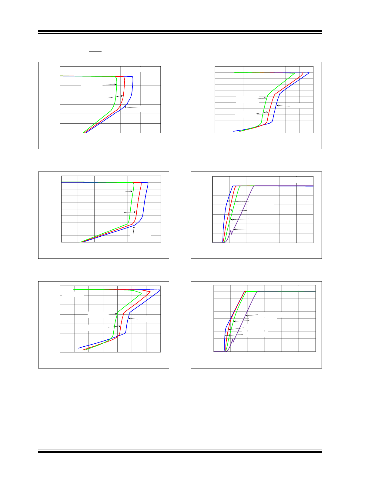
FIGURE 2-19:
Start-Up from SHDN.
FIGURE 2-20:
Start-Up from SHDN.
FIGURE 2-21:
Output Voltage vs. Output
Current.
FIGURE 2-22:
Output Voltage vs. Output
Current.
FIGURE 2-23:
Output Voltage vs. Output
Current.
FIGURE 2-24:
Output Voltage vs. Output
Current.
0V
4.3V
t
r
= 5 µs
Time = 80 µs/Div
V
OUT
(DC Coupled, 1V/Div)
V
R
= 3.3V
I
OUT
= 1 µA
I
OUT
= 10 mA
I
OUT
= 150 mA
SHDN
V
OUT
0V
6.0 V
t
r
= 5 µs
Time = 80 µs/Div
V
OUT
(DC Coupled, 2V/Div)
V
R
= 5.0V
I
OUT
= 1 µA
I
OUT
= 10 mA
I
OUT
= 150 mA
SHDN
V
OUT
0.00
0.20
0.40
0.60
0.80
1.00
1.20
1.40
0
50
100
150
200
250
Output V
o
lt
age
(V)
Output Current (mA)
V
IN
= 2.5V
V
IN
= 3.5V
V
IN
= 4.5V
V
IN
= 6.0V
V
R
= 1.2V
0.00
0.20
0.40
0.60
0.80
1.00
1.20
1.40
1.60
1.80
2.00
0
50
100
150
200
250
300
Output V
o
ltage (V)
Output Current (mA)
V
R
= 1.8V
V
IN
= 2.5V
V
IN
= 3.5V
V
IN
= 4.5V
V
IN
= 6.0V
0.00
0.50
1.00
1.50
2.00
2.50
3.00
3.50
0
50
100
150
200
250
300
350
Outpu
t V
o
ltag
e (V)
Output Current (mA)
V
IN
= 5.0V
V
IN
= 4.3V
V
IN
= 3.6V
V
IN
= 6.0V
V
R
= 3.3V
0.00
0.50
1.00
1.50
2.00
2.50
3.00
3.50
4.00
4.50
5.00
5.50
0
50
100
150
200
250
300
350
400
Ou
tpu
t V
o
ltag
e (V)
Output Current (mA)
V
IN
= 5.5V
V
IN
= 6.0V
V
R
= 5.0V
V
IN
= 5.5V
V
IN
= 6.0V
V
R
= 5.0V
V
IN
= 5.5V
V
IN
= 6.0V
V
R
= 5.0V
V
IN
= 5.5V
V
IN
= 5.2V
V
IN
= 6.0V
V
R
= 5.0V
MCP1711
DS20005415D-page 10
2015-2016 Microchip Technology Inc.
Note: Unless otherwise indicated, V
IN
= 3.5V for V
R
< 2.5V or V
IN
= V
R
+ 1V for V
R
2.5V, I
OUT
= 1 mA,
C
IN
= C
OUT
= 0 µF, V
SHDN
= V
IN
, T
A
= +25°C.
FIGURE 2-25:
Output Voltage vs. Output
Current.
FIGURE 2-26:
Output Voltage vs. Output
Current.
FIGURE 2-27:
Output Voltage vs. Output
Current.
FIGURE 2-28:
Output Voltage vs. Output
Current.
FIGURE 2-29:
Output Voltage vs. Input
Voltage.
FIGURE 2-30:
Output Voltage vs. Input
Voltage.
0.00
0.20
0.40
0.60
0.80
1.00
1.20
1.40
0
50
100
150
200
250
Output V
o
ltage (V)
Output Current (mA)
V
R
= 1.2V
T
A
= -40°C
T
A
= +85°C
T
A
= +25°C
0.00
0.20
0.40
0.60
0.80
1.00
1.20
1.40
1.60
1.80
2.00
0
50
100
150
200
250
300
Output V
o
ltage (V)
Output Current (mA)
V
R
= 1.8V
T
A
= +85°C
T
A
= +25°C
T
A
= -40°C
0.00
0.50
1.00
1.50
2.00
2.50
3.00
3.50
0
50
100
150
200
250
300
350
Ou
tpu
t V
o
ltag
e (V)
Output Current (mA)
V
R
= 3.3V
T
A
= +85°C
T
A
= +25°C
V
R
= 3.3V
T
A
= +85°C
T
A
= +25°C
V
R
= 3.3V
T
A
= +85°C
T
A
= +25°C
V
R
= 3.3V
T
A
= +85°C
T
A
= +25°C
V
R
= 3.3V
T
A
= +85°C
T
A
= +25°C
V
R
= 3.3V
T
A
= -40°C
T
A
= +85°C
T
A
= +25°C
V
R
= 3.3V
T
A
= +85°C
T
A
= +25°C
0.00
0.50
1.00
1.50
2.00
2.50
3.00
3.50
4.00
4.50
5.00
5.50
0
50
100
150
200
250
300
350
Output V
o
ltage (V)
Output Current (mA)
T
A
= +85°C
T
A
= +25°C
T
A
= +85°C
T
A
= +25°C
T
A
= +85°C
T
A
= +25°C
V
R
= 5.0V
T
A
= +85°C
T
A
= +25°C
T
A
= +85°C
T
A
= +25°C
T
A
= +85°C
T
A
= +25°C
T
A
= +85°C
T
A
= +25°C
T
A
= -40°C
T
A
= +85°C
T
A
= +25°C
0.00
0.20
0.40
0.60
0.80
1.00
1.20
1.40
0
1
2
3
4
5
6
Output V
o
ltage (V)
Input Voltage (V)
V
R
= 1.2V
I
OUT
= 1 µA
I
OUT
= 1 mA
I
OUT
= 10 mA
I
OUT
= 100 mA
0.00
0.20
0.40
0.60
0.80
1.00
1.20
1.40
1.60
1.80
2.00
0
1
2
3
4
5
6
Ou
tpu
t V
o
ltag
e (V)
Input Voltage (V)
V
R
= 1.8V
I
OUT
= 100 mA
I
OUT
= 1 µA
I
OUT
= 1 mA
I
OUT
= 10 mA