
2012-2015 Microchip Technology Inc.
DS20005158D-page 1
MCP1710
Features
• Ultra Low 20 nA (typical) Quiescent Current
• Ultra Low Shutdown Supply Current: 0.1 nA (typical)
• 200 mA Output Current Capability for V
R
≤ 3.5V
• 100 mA Output Current Capability for V
R
3.5V
• Input Operating Voltage Range: 2.5V to 5.5V
• Standard Output Voltages (V
R
):
- 1.2V, 1.5V, 1.8V, 2.0V, 2.5V, 3.0V, 3.3V, 4.2V
• Low Dropout Voltage: 450 mV Maximum at
200 mA
• Stable with 1.0 µF Ceramic Output Capacitor
• Overcurrent Protection
• Space-Saving, 8-Lead Plastic 2 x 2 VDFN
Applications
• Energy Harvesting
• Long Life Battery-Powered Applications
• Smart Cards
• Ultra Low Consumption “Green” Products
• Portable Electronics
Description
The MCP1710 is a 200 mA for V
R
≤ 3.5V, 100 mA for
V
R
3.5V, Low Dropout (LDO) linear regulator that
provides high-current and low-output voltages, while
maintaining an ultra low 20 nA of quiescent current
during device operation. In addition, the MCP1710 can
be shut down for an even lower 0.1 nA (typical) supply
current draw. The MCP1710 comes in eight standard,
fixed output voltage versions: 1.2V, 1.5V, 1.8V, 2V,
2.5V, 3V, 3.3V and 4.2V. The 200 mA output current
capability, combined with the low-output voltage
capability, make the MCP1710 a good choice for new
ultra long life LDO applications that have high-current
demands, but require ultra low-power consumption
during Sleep states.
The MCP1710 is stable using ceramic output
capacitors that inherently provide lower output noise,
and reduce the size and cost of the entire regulator
solution. Only 1 µF (2.2 µF recommended) of output
capacitance is needed to stabilize the LDO.
The MCP1710 device’s ultra low quiescent and
shutdown current allows it to be paired with other ultra
low-current draw devices, such as Microchip’s XLP
technology devices, for a complete ultra low-power
solution.
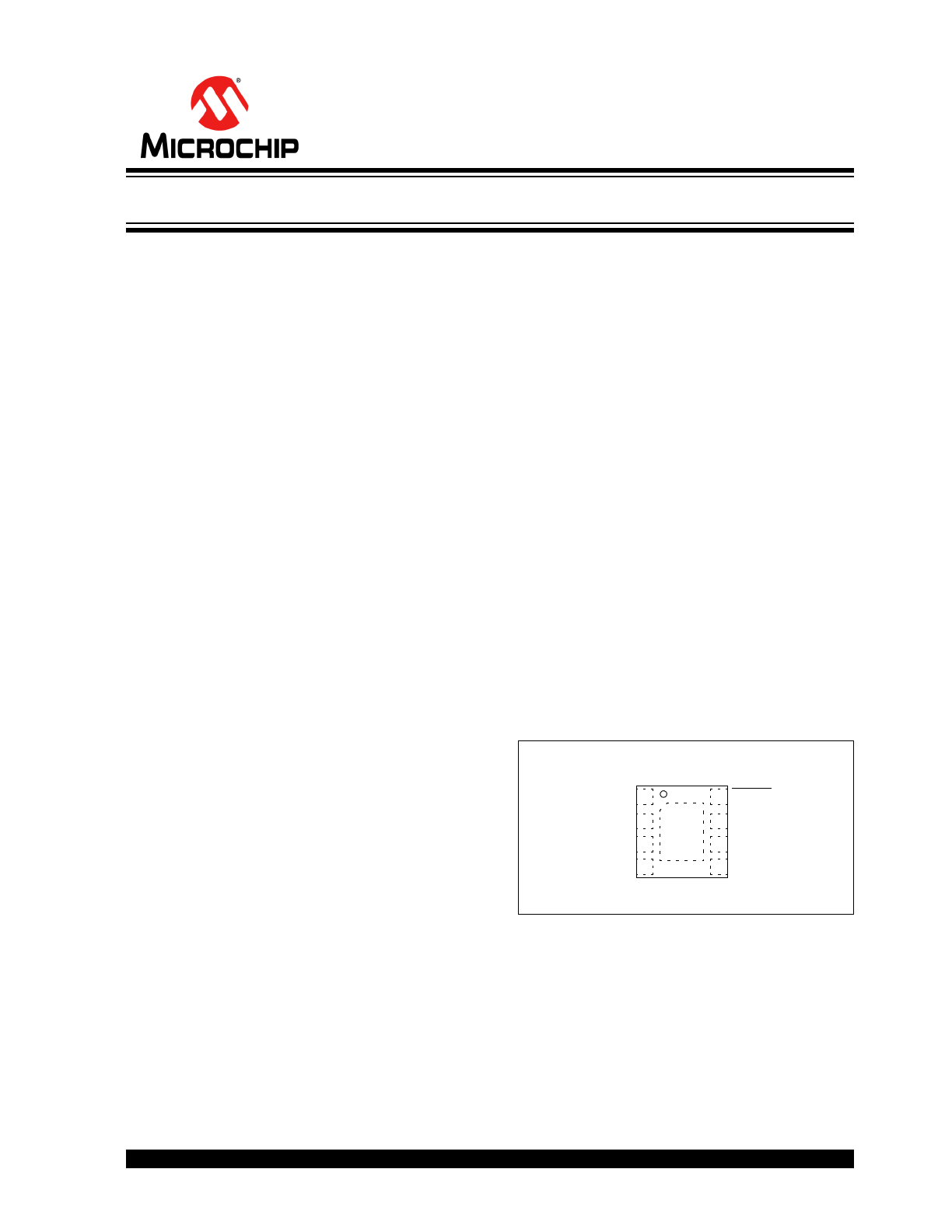
Package Type
MCP1710
2x2 VDFN*
NC
V
OUT
NC
V
IN
FB
1
2
3
4
8
7
6
5 NC
SHDN
GND
*
Includes Exposed Thermal Pad (EP); see
Table 3-1
.
EP
9
Ultra Low Quiescent Current LDO Regulator
MCP1710
DS20005158D-page 2
2012-2015 Microchip Technology Inc.
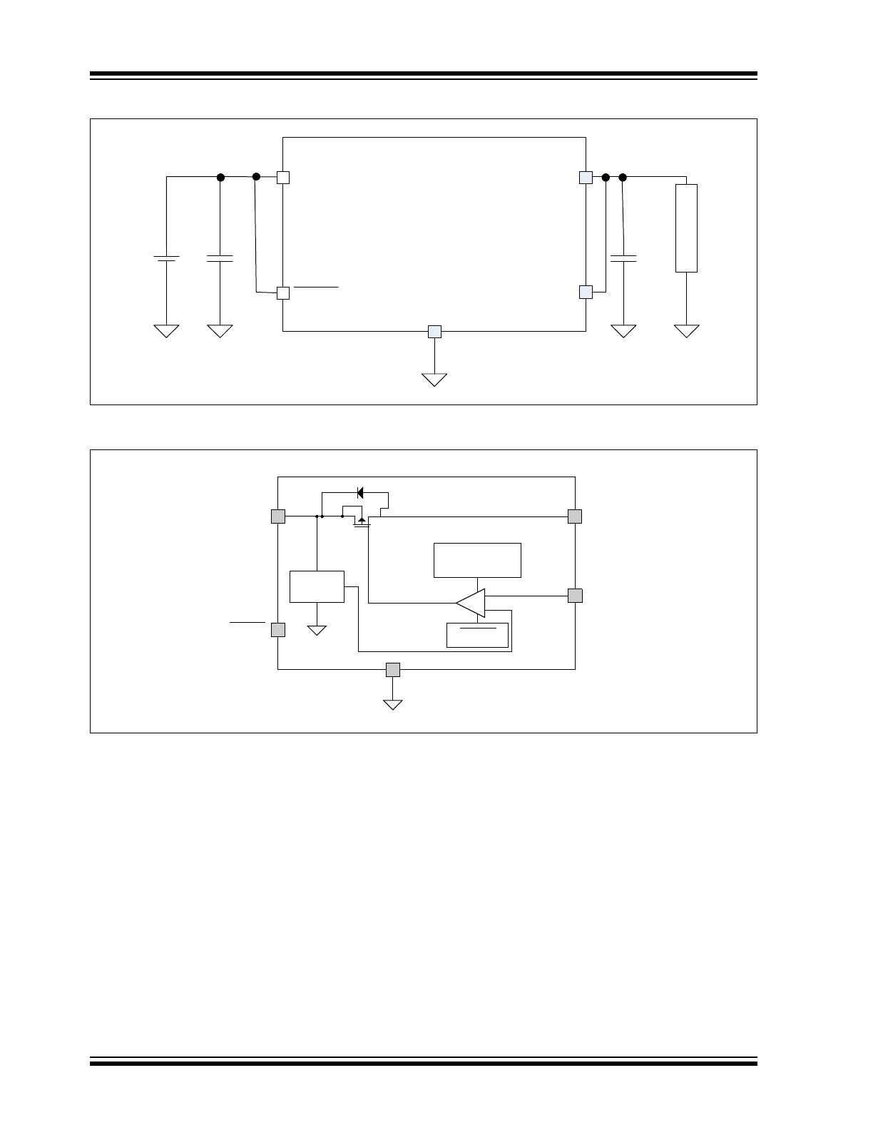
Typical Application
Functional Block Diagram
V
IN
V
OUT
FB
GND
LO
A
D
C
IN
C
OUT
SHDN
+
–
V
IN
SHDN
Voltage
Reference
Overcurrent
SHDN
GND
V
OUT
FB
+
–
2012-2015 Microchip Technology Inc.
DS20005158D-page 3
MCP1710
1.0
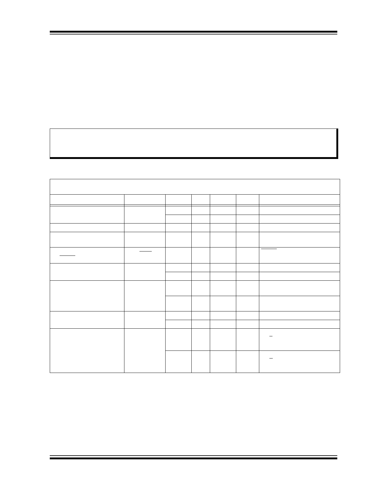
ELECTRICAL CHARACTERISTICS
Absolute Maximum Ratings
†
I
nput voltage, V
IN
................................................................................................................................................6.0V
Maximum voltage on any pin – GND ..................................................................................................... 0.3V to 6.0V
Output short-circuit duration............................................................................................ ............................Unlimited
Storage temperature ....................................................................................................................... -65°C to +150°C
Maximum junction temperature, T
J
................................................................................................................+150°C
Operating junction temperature, T
J
....................................................................................................-40°C to +85°C
ESD protection on all pins (HBM) ................................................................................................................... ≥ 2 kV
† Notice: Stresses above those listed under “Maximum Ratings” may cause permanent damage to the device. This
is a stress rating only and functional operation of the device at those or any other conditions above those indicated
in the operational listings of this specification is not implied. Exposure to maximum rating conditions for extended
periods may affect device reliability.
AC/DC CHARACTERISTICS
Electrical Specifications: Unless otherwise noted, V
IN
= V
R
+ 800 mV (
Note 1
), I
OUT
= 1 mA, C
IN
= C
OUT
= 2.2 µF
(X7R Ceramic), T
A
= +25°C. Boldface type applies for junction temperatures T
J
of -40°C to +85°C (
Note 4
).
Parameters
Sym.
Min.
Typ.
Max.
Units
Conditions
Input Operating Voltage
V
IN
2.7
—
5.5
V
2.5
—
5.5
V
V
R
< 2.5V
Output Voltage Range
V
OUT
1.2
—
4.2
V
Input Quiescent Current
I
Q
—
20
—
nA
V
IN
= 2.5V to 5.5V,
I
OUT
= 0
Input Quiescent Current
for SHDN Mode
I
SHDN
—
0.1
—
nA
SHDN = GND
Maximum Continuous
Output Current
I
OUT
—
—
200
mA
V
R
≤ 3.5V
—
—
100
mA
V
R
3.5V
Current Limit
I
OUT
—
250
—
mA
V
OUT
= 0.9 x V
R
,
V
R
≤ 3.5V
—
175
—
mA
V
OUT
= 0.9 x V
R
,
V
R
3.5V
Output Voltage Regulation
V
OUT
V
R
– 4%
—
V
R
+ 4%
V
V
R
< 1.8V (
Note 2
)
V
R
– 2%
—
V
R
+ 2%
V
V
R
≥ 1.8V (
Note 2
)
Line Regulation
V
OUT
/
(V
OUT
x
V
IN
)
—
0.5
4
%
V
IN
= V
IN(Min)
to 5.5V,
V
R
≥ 1.8V, I
OUT
= 50 mA
(
Note 1
)
—
—
4
%
V
IN
= V
IN(Min)
to 5.5V,
V
R
< 1.8V, I
OUT
= 50 mA
(
Note 1
)
Note 1:
The minimum V
IN
must meet two conditions: V
IN
V
IN(Min)
and V
IN
V
R
V
DROPOUT(Max).
2:
V
R
is the nominal regulator output voltage. V
R
= 1.2V, 2.5V, etc.
3:
Dropout voltage is defined as the input-to-output voltage differential at which the output voltage drops 3%
below its nominal value that was measured with an input voltage of V
IN
= V
OUT(Max)
+ V
DROPOUT(Max)
.
4:
The junction temperature is approximated by soaking the device under test at an ambient temperature
equal to the desired junction temperature. The test time is small enough such that the rise in the junction
temperature over the ambient temperature is not significant.
MCP1710
DS20005158D-page 4
2012-2015 Microchip Technology Inc.
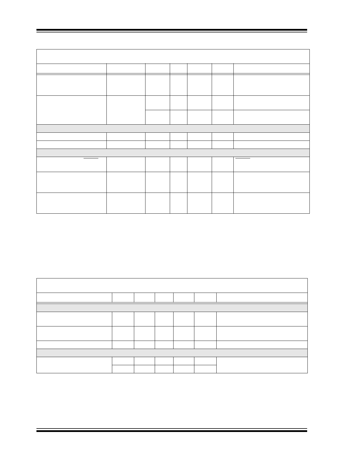
Load Regulation
V
OUT
/V
OUT
—
1
3
%
V
IN
= (V
IN(Min)
+ V
IN(Max)
)/2,
I
OUT
= 0.02 mA to 200 mA
(
Note 1
)
Dropout Voltage
V
DROPOUT
—
—
450
mV
I
OUT
= 200 mA,
V
R
≤ 3.5V (
Note 3
)
—
—
400
mV
I
OUT
= 100 mA,
V
R
> 3.5V (
Note 3
)
Shutdown Input
Logic High Input
V
SHDN-HIGH
70
—
—
%V
IN
V
IN
= V
IN(Min)
to 5.5V (
Note 1
)
Logic Low Input
V
SHDN-LOW
—
—
30
%V
IN
V
IN
= V
IN(Min)
to 5.5V (
Note 1
)
AC Performance
Output Delay From SHDN
T
OR
—
30
—
ms
SHDN = GND to V
IN
,
V
OUT
= GND to 95% V
R
Output Noise
e
N
—
0.37
—
µV/
Hz I
OUT
= 50 mA, f = 1 kHz,
C
OUT
= 2.2 µF (X7R Ceramic),
V
R
= 2.5V
Power Supply Ripple
Rejection Ratio
PSRR
—
22
—
dB
f = 100 Hz, I
OUT
= 10 mA,
V
INAC
= 200 mV pk-pk,
C
IN
= 0 µF
TEMPERATURE SPECIFICATIONS
Electrical Specifications: Unless otherwise noted, V
IN
= V
R
+ 800 mV, (
Note 1
), I
OUT
= 1 mA, C
IN
= C
OUT
= 2.2 µF
(X7R Ceramic), T
A
= +25°C. Boldface type applies for junction temperatures, T
J
of -40°C to +85°C (
Note 4
)
Parameters
Sym.
Min.
Typ.
Max.
Units
Conditions
Temperature Ranges
Operating Junction
Temperature Range
T
J
-40
—
+85
°C
Steady state
Maximum Junction
Temperature
T
J
—
—
+150
°C
Transient
Storage Temperature Range
T
A
-65
—
+150
°C
Thermal Package Resistances
Thermal Resistance,
2 x 2 VDFN-8
JA
—
73.1
—
°C/W
JEDEC
®
standard FR4 board with
1 oz copper and thermal vias
JC
—
10.7
—
°C/W
AC/DC CHARACTERISTICS (CONTINUED)
Electrical Specifications: Unless otherwise noted, V
IN
= V
R
+ 800 mV (
Note 1
), I
OUT
= 1 mA, C
IN
= C
OUT
= 2.2 µF
(X7R Ceramic), T
A
= +25°C. Boldface type applies for junction temperatures T
J
of -40°C to +85°C (
Note 4
).
Parameters
Sym.
Min.
Typ.
Max.
Units
Conditions
Note 1:
The minimum V
IN
must meet two conditions: V
IN
V
IN(Min)
and V
IN
V
R
V
DROPOUT(Max).
2:
V
R
is the nominal regulator output voltage. V
R
= 1.2V, 2.5V, etc.
3:
Dropout voltage is defined as the input-to-output voltage differential at which the output voltage drops 3%
below its nominal value that was measured with an input voltage of V
IN
= V
OUT(Max)
+ V
DROPOUT(Max)
.
4:
The junction temperature is approximated by soaking the device under test at an ambient temperature
equal to the desired junction temperature. The test time is small enough such that the rise in the junction
temperature over the ambient temperature is not significant.
2012-2015 Microchip Technology Inc.
DS20005158D-page 5
MCP1710
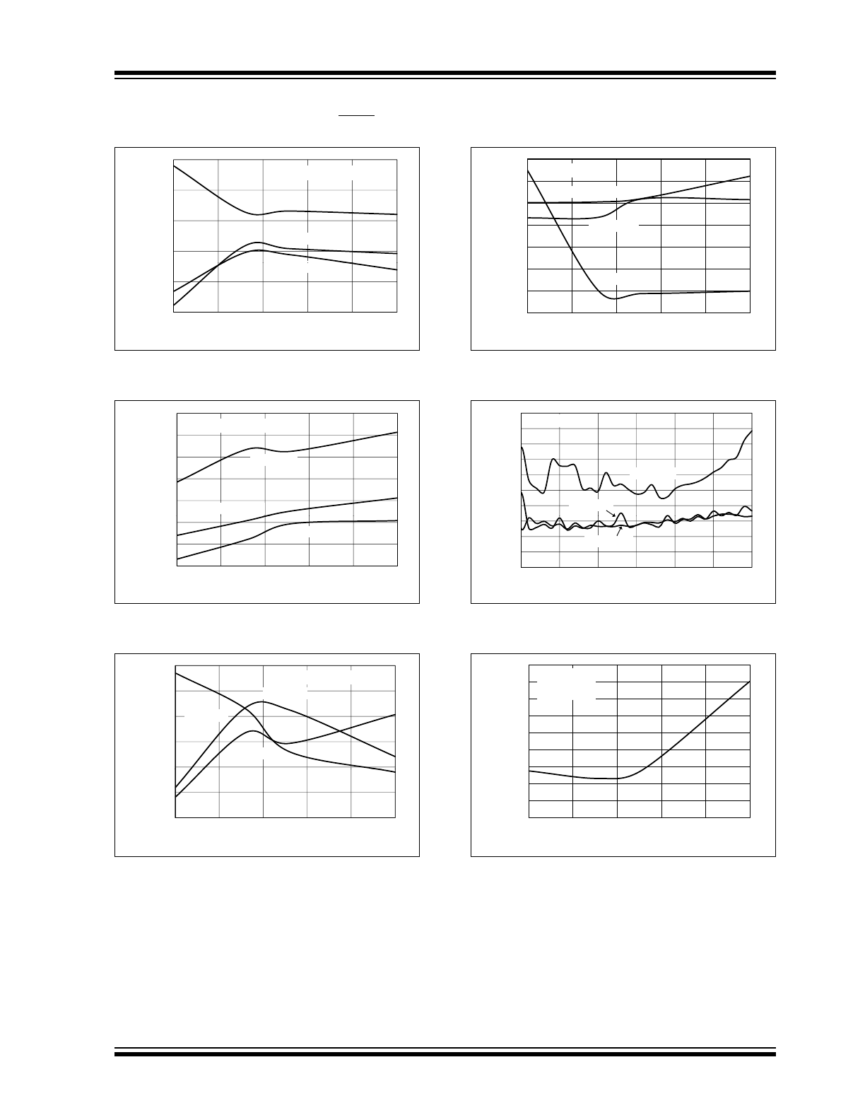
2.0
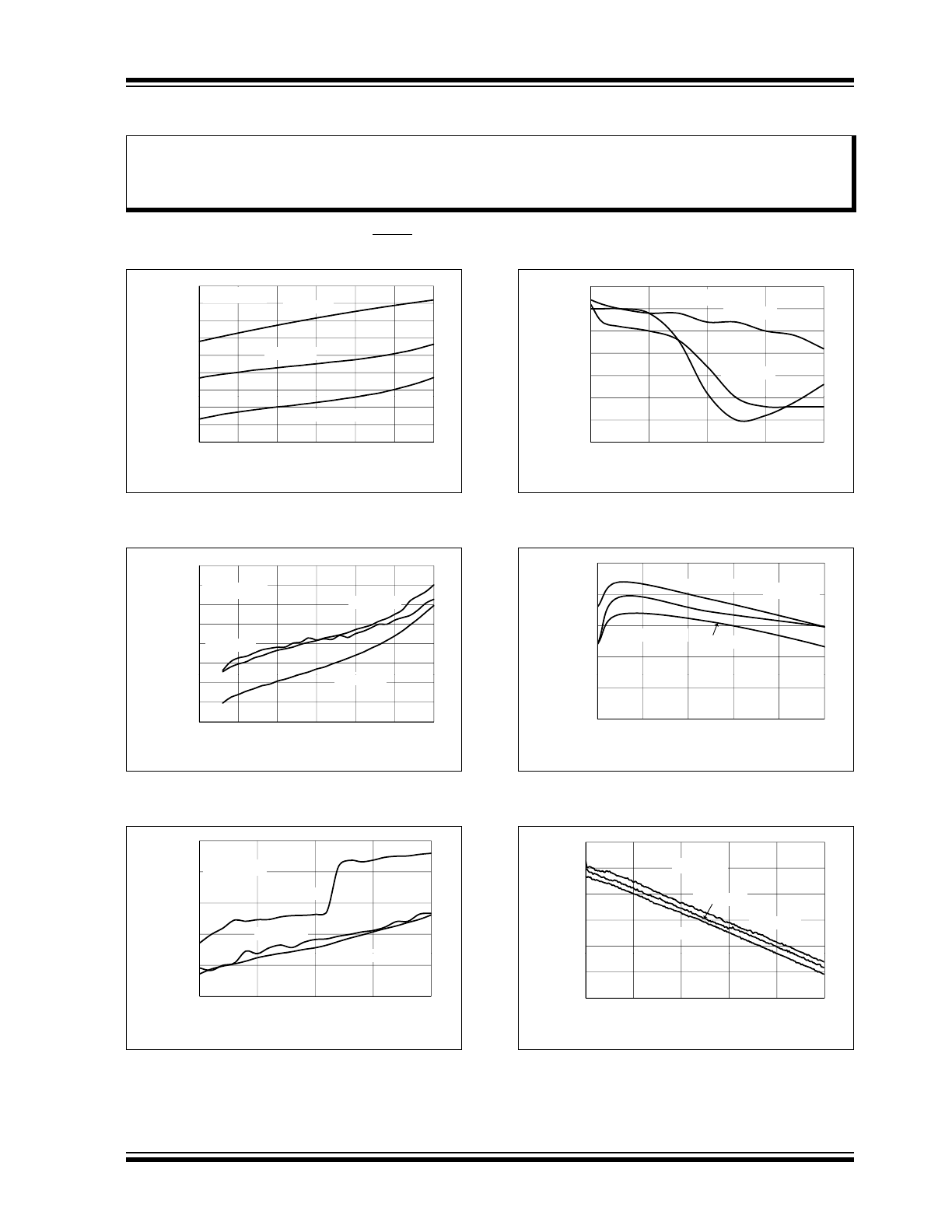
TYPICAL PERFORMANCE CURVES
Note: Unless otherwise indicated,
C
OUT
= 2.2 µF Ceramic (X7R), C
IN
= 2.2 µF Ceramic (X7R), I
OUT
= 1 mA,
Temperature = +25°C, V
IN
= V
R
+ 0.8V, SHDN = 1 M
pull-up to V
IN
.
FIGURE 2-1:
Output Voltage vs. Input
Voltage (V
R
= 1.2V).
FIGURE 2-2:
Output Voltage vs. Input
Voltage (V
R
= 2.5V).
FIGURE 2-3:
Output Voltage vs. Input
Voltage (V
R
= 4.2V).
FIGURE 2-4:
Output Voltage vs. Load
Current (V
R
= 1.2V).
FIGURE 2-5:
Output Voltage vs. Load
Current (V
R
= 2.5V).
FIGURE 2-6:
Output Voltage vs. Load
Current (V
R
= 4.2V).
Note:
The graphs and tables provided following this note are a statistical summary based on a limited number of
samples and are provided for informational purposes only. The performance characteristics listed herein
are not tested or guaranteed. In some graphs or tables, the data presented may be outside the specified
operating range (e.g., outside specified power supply range) and therefore outside the warranted range.
1.210
1.215
1.220
1.225
1.230
1.235
1.240
tput V
o
ltage
(V)
T
J
= +25°C
I
OUT
= 0.1 mA
T
J
= -40°C
1.195
1.200
1.205
2.5
3.0
3.5
4.0
4.5
5.0
5.5
Ou
t
Input Voltage (V)
T
J
= +85°C
2.500
2.502
2.504
2.506
2.508
2.510
tput V
o
ltage
(V)
T
J
= +25°C
I
OUT
= 0.1 mA
T
J
= -40°C
2.494
2.496
2.498
2.5
3.0
3.5
4.0
4.5
5.0
5.5
Ou
t
Input Voltage (V)
T
J
= +85°C
4.240
4.244
4.248
4.252
u
tput V
o
ltage
(V)
T
J
= -40°C
T
85°C
T
J
= +25°C
I
OUT
= 0.1 mA
4.232
4.236
4.50
4.75
5.00
5.25
5.50
O
u
Input Voltage (V)
T
J
= +85°C
1 180
1.185
1.190
1.195
1.200
1.205
tput V
o
ltage
(V)
T
J
= +25°C
T
J
= +85°C
V
IN
= 2.5V
1.170
1.175
1.180
0
50
100
150
200
Ou
t
Load Current (mA)
T
J
= -40°C
2.4950
2.4975
2.5000
2.5025
u
tput V
o
ltage
(V)
T
J
= +25°C
T
J
= +85°C
V
IN
= 3.3V
T
J
= -40°C
2.4900
2.4925
0
20
40
60
80
100
O
u
Load Current (mA)
4.21
4.22
4.23
4.24
4.25
u
tput V
o
ltage
(V)
T
J
= +25°C
T
J
= +85°C
V
IN
= 4.15V
T
J
= -40°C
4.19
4.20
0
20
40
60
80
100
O
u
Load Current (mA)
MCP1710
DS20005158D-page 6
2012-2015 Microchip Technology Inc.
Note: Unless otherwise indicated,
C
OUT
= 2.2 µF Ceramic (X7R), C
IN
= 2.2 µF Ceramic (X7R), I
OUT
= 1 mA,
Temperature = +25°C, V
IN
= V
R
+ 0.8V, SHDN = 1 M
pull-up to V
IN
.
FIGURE 2-7:
Dropout Voltage vs. Load
Current (V
R
= 2.5V).
FIGURE 2-8:
Dropout Voltage vs. Load
Current (V
R
= 4.2V).
FIGURE 2-9:
Noise vs. Frequency.
FIGURE 2-10:
Power Supply Ripple
Rejection vs. Frequency (V
R
= 1.2V).
FIGURE 2-11:
Power Supply Ripple
Rejection vs. Frequency (V
R
= 2.5V).
FIGURE 2-12:
Power Supply Ripple
Rejection vs. Frequency (V
R
= 4.2V).
0.00
0.05
0.10
0.15
0.20
0.25
0.30
0
20
40
60
80
100
Dropout V
o
ltage (V)
Load Current (mA)
T
J
= +85°C
T
J
= -40°C
T
J
= +25°C
V
OUT
= 2.5V
0.08
0.10
0.12
0.14
0.16
0.18
0.20
p
out V
o
ltage (V)
T
J
= +85°C
T
J
= -40°C
T
J
= +25°C
V
OUT
= 4.2V
0.00
0.02
0.04
0.06
0
20
40
60
80
100
Dro
p
Load Current (mA)
ut Noise
(μV/
¥Hz)
V
IN
= 5.2V
V
OUT
= 4.2V
I
OUT
= 50 mA
0.1
1
10
V
IN
= 3.5V
V
OUT
= 2.5V
I
OUT
= 50 mA
V
IN
= 2.8V
V
OUT
= 1.8V
I
OUT
= 50 mA
Outp
u
Frequency (kHz)
0.01
0.1
0.01
0.1
1
10
100
1000
-60
-50
-40
-30
-20
-10
0
10
P
SRR (dB)
V
IN
= 2.5V
I
OUT
= 10 mA
-100
-90
-80
-70
0.01
0.1
1
10
100
1000
P
Frequency (kHz)
-60
-50
-40
-30
-20
-10
0
10
PSRR (dB)
V
IN
= 3.5V
I
OUT
= 10 mA
-100
-90
-80
-70
0.01
0.1
1
10
100
1000
Frequency (kHz)
-60
-50
-40
-30
-20
-10
0
10
PSRR (dB)
V
IN
= 5.2V
I
OUT
= 10 mA
-100
-90
-80
-70
0.01
0.1
1
10
100
1000
Frequency (kHz)
2012-2015 Microchip Technology Inc.
DS20005158D-page 7
MCP1710
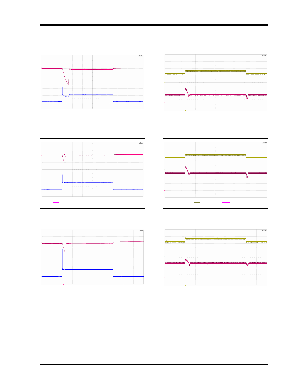
Note: Unless otherwise indicated,
C
OUT
= 2.2 µF Ceramic (X7R), C
IN
= 2.2 µF Ceramic (X7R), I
OUT
= 1 mA,
Temperature = +25°C, V
IN
= V
R
+ 0.8V, SHDN = 1 M
pull-up to V
IN
.
FIGURE 2-13:
Dynamic Load Step
(V
R
= 1.2V).
FIGURE 2-14:
Dynamic Load Step
(V
R
= 2.5V).
FIGURE 2-15:
Dynamic Load Step
(V
R
= 4.2V).
FIGURE 2-16:
Dynamic Line Step
(V
R
= 1.2V).
FIGURE 2-17:
Dynamic Line Step
(V
R
= 2.5V).
FIGURE 2-18:
Dynamic Line Step
(V
R
= 4.2V).
V
OUT
= 1.2V
I
OUT
= 100 nA to 10 mA
CH1 (AC) 200 mV/div
CH2 10 mA/div
200 µs/div
CH1
CH2
V
OUT
= 2.5V
I
OUT
= 100 nA to 10 mA
AC1M 200 mV/div
10 mA/div
200 µs/div
V
OUT
= 4.2V
I
OUT
= 100 nA to 10 mA
AC1M 200 mV/div
10 mA/div
200 µs/div
I
OUT
= 10 mA
V
IN
= 2.5V to 3.5V
2V/div
1V/div
V
OUT
= 1.2V
10 ms/div
I
OUT
= 10 mA
V
IN
= 3.5V to 4.5V
2V/div
1V/div
V
OUT
= 2.5V
10 ms/div
I
OUT
= 10 mA
V
IN
= 4.5V to 5.5V
2V/div
2V/div
V
OUT
= 4.2V
10 ms/div
MCP1710
DS20005158D-page 8
2012-2015 Microchip Technology Inc.
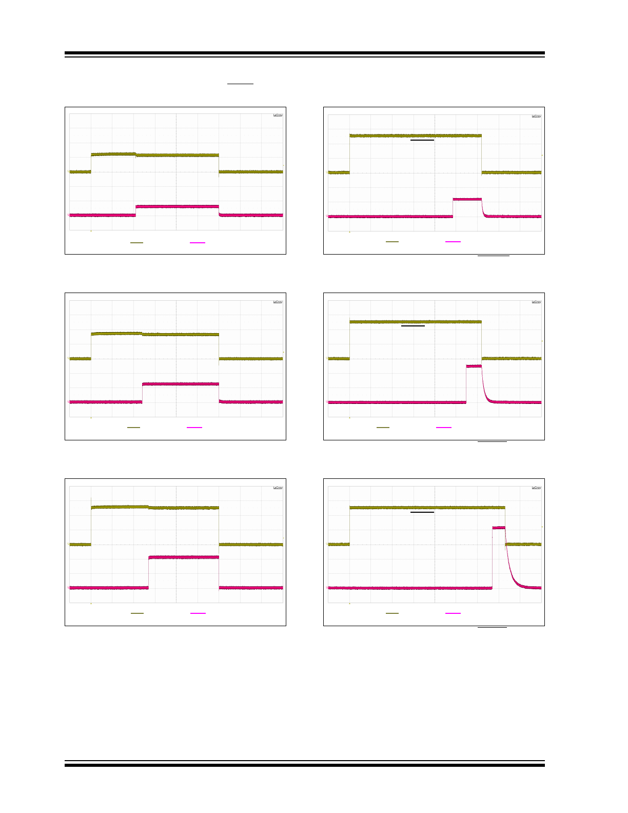
Note: Unless otherwise indicated,
C
OUT
= 2.2 µF Ceramic (X7R), C
IN
= 2.2 µF Ceramic (X7R), I
OUT
= 1 mA,
Temperature = +25°C, V
IN
= V
R
+ 0.8V, SHDN = 1 M
pull-up to V
IN
.
FIGURE 2-19:
Start-up from V
IN
(V
R
= 1.2V).
FIGURE 2-20:
Start-up from V
IN
(V
R
= 2.5V).
FIGURE 2-21:
Start-up from V
IN
(V
R
= 4.2V).
FIGURE 2-22:
Start-up from SHDN
(V
R
= 1.2V).
FIGURE 2-23:
Start-up from SHDN
(V
R
= 2.5V).
FIGURE 2-24:
Start-up from SHDN
(V
R
= 4.2V).
I
OUT
= 100 nA
V
IN
= 2.5V
2V/div
2V/div
V
OUT
= 1.2V
10 ms/div
I
OUT
= 100 nA
V
IN
= 3.5V
2V/div
2V/div
V
OUT
= 2.5V
10 ms/div
I
OUT
= 100 nA
V
IN
= 5.2V
2V/div
2V/div
V
OUT
= 4.2V
10 ms/div
I
OUT
= 10 mA
SHDN Signal
2V/div
1V/div
V
OUT
= 1.2V
5 ms/div
I
OUT
= 10 mA
SHDN Signal
2V/div
1V/div
V
OUT
= 2.5V
5 ms/div
I
OUT
= 10 mA
SHDN Signal
2V/div
1V/div
V
OUT
= 4.2V
5 ms/div
2012-2015 Microchip Technology Inc.
DS20005158D-page 9
MCP1710
Note: Unless otherwise indicated,
C
OUT
= 2.2 µF Ceramic (X7R), C
IN
= 2.2 µF Ceramic (X7R), I
OUT
= 1 mA,
Temperature = +25°C, V
IN
= V
R
+ 0.8V, SHDN = 1 M
pull-up to V
IN
.
FIGURE 2-25:
Load Regulation vs.
Junction Temperature (V
R
= 1.2V).
FIGURE 2-26:
Load Regulation vs.
Junction Temperature (V
R
= 2.5V).
FIGURE 2-27:
Load Regulation vs.
Junction Temperature (V
R
= 4.2V).
FIGURE 2-28:
Line Regulation vs. Junction
Temperature.
FIGURE 2-29:
Quiescent Current vs. Input
Voltage.
FIGURE 2-30:
Ground Current vs. Junction
Temperature.
0.50
1.00
1.50
2.00
d
Regulation (%
)
V
IN
= 2.5V
V
IN
= 4.0V
I
OUT
= 0 mA to 100 mA
-0.50
0.00
-40
-15
10
35
60
85
Loa
d
Junction Temperature (°C)
V
IN
= 5.5V
-0.10
0.00
0.10
0.20
0.30
d
Regulation (%
)
V
IN
= 2.8V
I
OUT
= 0 mA to 100 mA
V
IN
= 4.0V
-0.40
-0.30
-0.20
-40
-15
10
35
60
85
Loa
d
Junction Temperature (°C)
V
IN
= 5.5V
0.01
0.02
0.03
0.04
0.05
d
Regulation (%
)
V
IN
= 5.0V
I
OUT
= 0 mA to 100 mA
V
IN
= 4.5V
V
IN
= 5.5V
-0.01
0.00
0.01
-40
-15
10
35
60
85
Loa
d
Junction Temperature (°C)
0.15
0.20
0.25
0.30
0.35
0.40
0.45
0.50
-40
-15
10
35
60
85
Line Regulation (%
/V)
Junction Temperature (°C)
I
OUT
= 1 mA
V
OUT
= 4.2V
V
OUT
= 2.5V
V
OUT
= 1.2V
20
25
30
35
40
45
50
c
ent Current (nA)
T
J
= +85°C
T
J
= -40°C
V
OUT
= 1.2V
0
5
10
15
2.5
3.0
3.5
4.0
4.5
5.0
5.5
Quies
c
Input Voltage (V)
T
J
= +25°C
0.50
0.55
0.60
0.65
0.70
0.75
0.80
0.85
0.90
0.95
-40
-15
10
35
60
85
Ground Current (µA)
Junction Temperature (°C)
V
IN
= 2.5V
V
OUT
= 1.2V
I
OUT
= 0.1 mA
MCP1710
DS20005158D-page 10
2012-2015 Microchip Technology Inc.
Note: Unless otherwise indicated,
C
OUT
= 2.2 µF Ceramic (X7R), C
IN
= 2.2 µF Ceramic (X7R), I
OUT
= 1 mA,
Temperature = +25°C, V
IN
= V
R
+ 0.8V, SHDN = 1 M
pull-up to V
IN
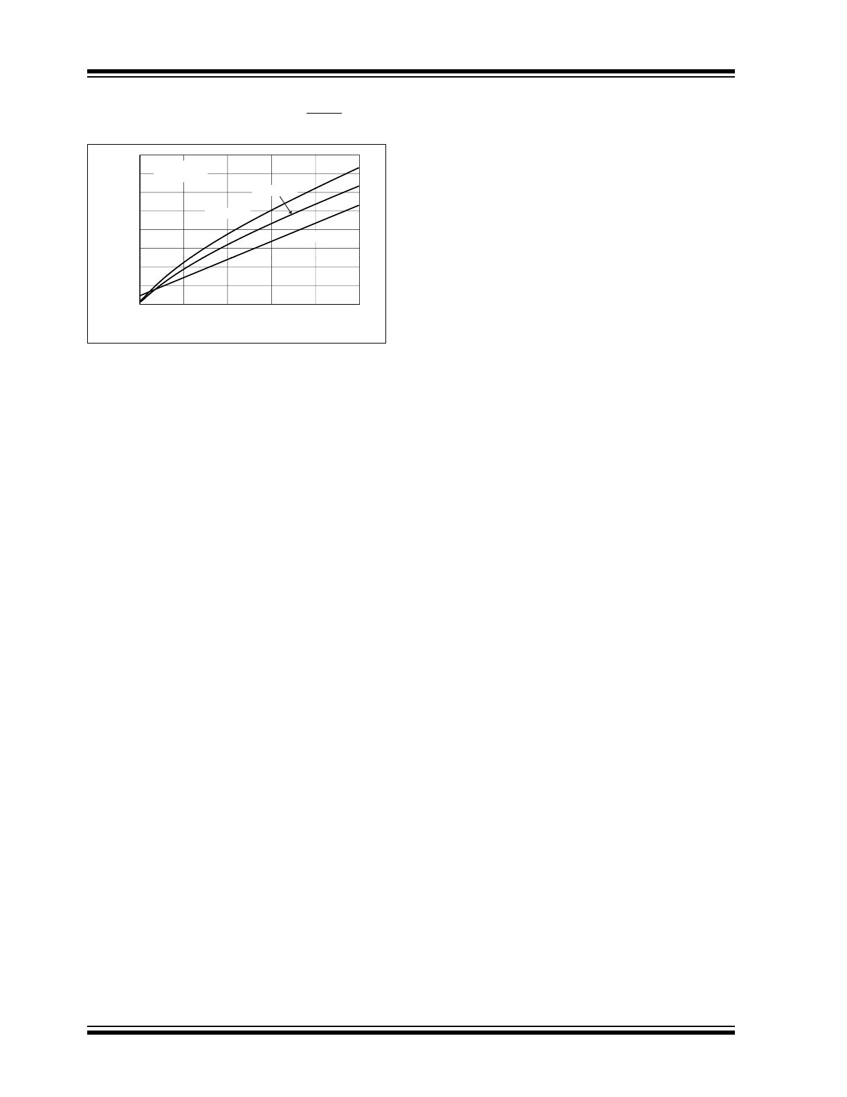
.
FIGURE 2-31:
Ground Current vs. Load
Current.
60
80
100
120
140
160
u
nd Current (µA)
T
J
= +85°C
T
J
= +25°C
T
J
= -40°C
V
IN
= 4.0V
V
OUT
= 1.2V
0
20
40
0
20
40
60
80
100
Gro
u
Load Current (mA)