
2017 Microchip Technology Inc.
DS20005872A-page 1
MCP1665
Features
• 36V, 100 m
Integrated Switch
• Up to 92% Efficiency
• Higher Current Compared to the Previous
MCP166x Switchers Family
• Output Voltage Range: Up to 32V
• 3.6A Typical Peak Input Current Limit:
- I
OUT
> 1 A at 5.0V V
IN
, 12V V
OUT
- I
OUT
> 700 mA at 3.3V V
IN
, 12V V
OUT
- I
OUT
> 400 mA at 4.2V V
IN
, 24V V
OUT
• Input Voltage Range: 2.9V to 5V
• Input Undervoltage Lockout (UVLO):
- UVLO at V
IN
Rising: 2.9V, typical
- UVLO at V
IN
Falling: 2.7V, typical
• No Load Input Current: 250 µA Typically for
Pulse-Frequency Modulation (PFM), 500 µA
Typically for Pulse-Width Modulation (PWM)
• Shutdown Mode with 0.4 µA Typical Quiescent
Current
• Automatically PFM/PWM or Selected by the
MODE Pin, for High Efficiency
• 500 kHz PWM Operation with Skipping Mode
Operation Selectable by Dedicated MODE Pin
• Feedback Voltage Reference: V
FB
= 1.2V
• Cycle-by-Cycle Current Limiting
• Internal Compensation
• Inrush Current Limiting and Internal Soft Start
• Output Overvoltage Protection (OVP) and Open-
Load Protection
(OLP) for Constant Current
Configuration
• Thermal Shutdown
• Easily Configurable for Single-ended Primary-
inductor Converter (SEPIC), Cuk or Flyback
Topologies
• Available Package: 10-Lead 2x2 mm VQFN
Applications
• Three-Cell Alkaline, Lithium and NiMH/NiCd
Portable Products
• Single-Cell Li-Ion to 5V, 12V or 24V Converters
• LCD Bias Supply for Portable Applications
• Camera Phone Flash
• Flashlight
• Battery-Powered LEDs
• Lighting Applications
• Portable Medical Equipment
• Hand-Held Instruments
General Description
The MCP1665 device is a compact, high-efficiency,
fixed-frequency, nonsynchronous step-up DC-DC
converter that integrates a 36V, 100 m
NMOS switch.
It provides a space-efficient high-voltage step-up
power supply solution for applications powered by
either three-cell alkaline, Ultimate Lithium, NiCd, NiMH,
one-cell Li-Ion or Li-Polymer batteries.
The integrated switch is protected by the typical 3.6A
cycle-by-cycle inductor peak current limit operation.
There is an output overvoltage protection and an open-
load protection that turn off switching so that if the
feedback resistors are accidentally disconnected, the
feedback pin is short-circuited to GND or the output is
exposed to excessive voltage.
Soft Start circuit allows the regulator to start-up without
high inrush current or output voltage overshoot from a
low-voltage input. The device features an UVLO which
avoids start-up and operation with low inputs or
discharged batteries for cell-powered applications. A
PFM switching mode (used for power saving) is
implemented and it is selectable by the dedicated
MODE pin.
For standby applications (EN = GND), the device stops
switching, enters Shutdown mode and consumes
0.4 µA of (typical) input current (feedback divider
current not included).
MCP1665 is easy to use and allows creating classic
boost, SEPIC or flyback DC-DC converters within a
small Printed Circuit Board (PCB) area. All
compensation and protection circuitry are integrated to
minimize the number of external components. Ceramic
input and output capacitors are used.
Package Types
*Includes Exposed Thermal Pad (EP); see
Table 3-1
S
GND
P
GND
FB
SW
EN
1
2
3
4
9
8
7
6 V
IN
SW
P
GND
EP
0
P
GND
MODE
10
5
MCP1665
2 x 2 mm VQFN*
High-Voltage 3.6A Integrated Switch PFM/PWM Boost Regulator
MCP1665
DS20005872A-page 2
2017 Microchip Technology Inc.
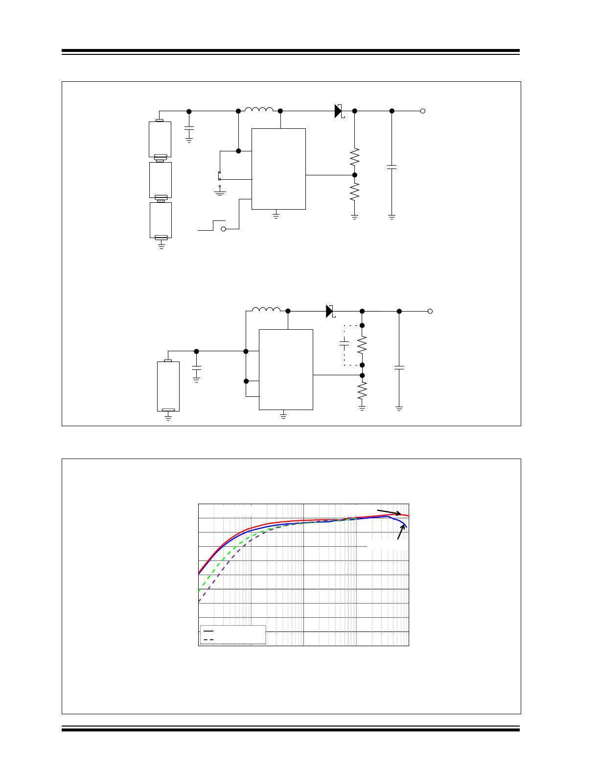
Typical Applications
Best Efficiency vs. I
OUT
GND
V
FB
V
OUT
24V, >350 mA
C
OUT
4x10 µF
C
IN
2x10 µF
L
10 µH
SW
383 k
20
k
EN
+
-
Li-Ion
R
TOP
R
BOT
V
IN
3.3V-4.2V
D
V
IN
MCP1665
40V 1A
MODE
C
TOP
15 pF
V
IN
GND
V
FB
V
OUT
12V 1 A
C
OUT
4x10 µF
C
IN
2x10 µF
L
SW
1
80 k
20 k
EN
+
-
Ni
-C
d
ON
OFF
R
TOP
R
BOT
V
IN
3
.6V-4.2V
D
MCP1665
MODE
U1
+
-
Ni
-C
d
+
-
Ni
-C
d
4.7 µH
20V 2A
PFM/PWM
PWM Only
0
10
20
30
40
50
60
70
80
90
100
0.1
1
10
100
1000
Eff
ici
ency (
%
)
I
OUT
(mA)
V
OUT
=12V
V
IN
=3.6V
PWM/PFM
PWM ONLY
V
IN
=5V
2017 Microchip Technology Inc.
DS20005872A-page 3
MCP1665
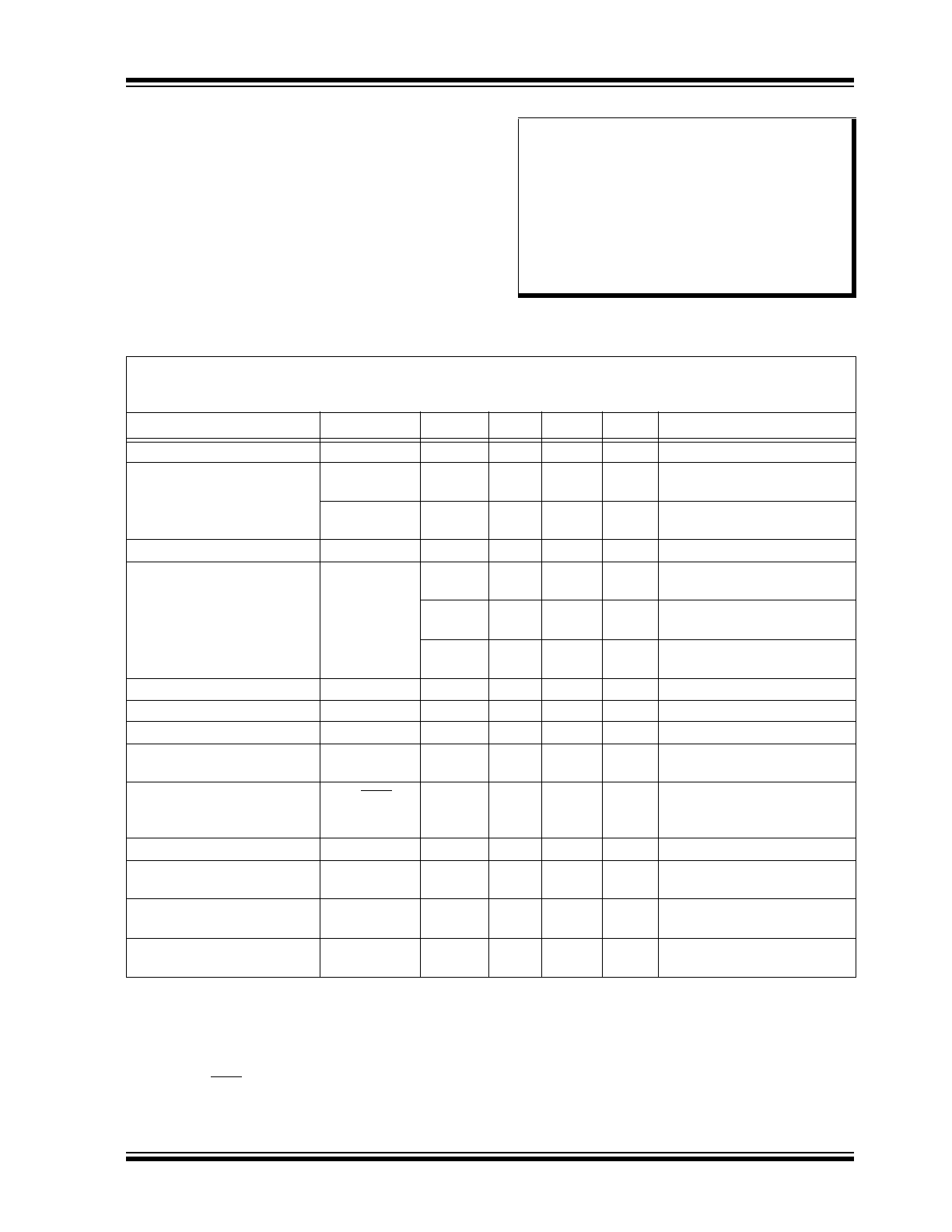
1.0
ELECTRICAL
CHARACTERISTICS
Absolute Maximum Ratings
EN, V
IN,
V
FB
– GND ........................................................+5.5V
V
SW
– GND .....................................................................+36V
Power Dissipation ....................................... Internally Limited
Storage Temperature ................................... –65°C to +150°C
Ambient Temperature with Power Applied ... –40°C to +125°C
Operating Junction Temperature.................. –40°C to +150°C
ESD Protection On All Pins:
HBM................................................................. 4 kV
MM..................................................................300V
Note:
Stresses above those listed under “Maxi-
mum Ratings” may cause permanent
damage to the device. This is a stress rat-
ing only and functional operation of the
device at those or any other conditions
above those indicated in the operational
sections of this specification is not
intended. Exposure to maximum rating
conditions for extended periods may
affect the device’s reliability.
TABLE 1-1:
DC AND AC CHARACTERISTICS
Electrical Specifications: Unless otherwise specified, all limits apply for typical values at ambient temperature
T
A
= +25°C, V
IN
= 3.6V, I
OUT
= 25 mA, V
OUT
= 12V, C
IN
= 22 µF, C
OUT
= 40 µF, X7R ceramic, L = 4.7 µH.
Boldface specifications apply over the controlled T
A
range of –40°C to +125°C.
Parameters
Sym.
Min.
Typ.
Max.
Units
Conditions
Input Voltage Range
V
IN
2.7
—
5
V
Note 1
Undervoltage Lockout
(UVLO)
UVLO
START
2.7
2.85
3
V
V
IN
rising,
I
OUT
= 25 mA resistive load
UVLO
STOP
2.5
2.65
2.8
V
V
IN
falling,
I
OUT
= 25 mA resistive load
Output Voltage Adjust Range
V
OUT
V
IN
+1V
—
32
V
Note 1
Maximum Output Current
I
OUT
—
1000
—
mA
5.0V V
IN
, 12V V
OUT
10% drop (
Note 4
)
—
700
—
mA
3.3V V
IN
, 12V V
OUT
10% drop
(
Note 4
)
—
400
—
mA
4.2V V
IN
, 24V V
OUT
10% drop (
Note 4
)
Feedback Voltage
V
FB
1.164
1.2
1.236
V
—
V
FB
Accuracy
—
-3
—
3
%
—
Feedback Input Bias Current
I
VFB
—
10
—
nA
—
No Load Input Current (PFM)
I
IN0
—
250
—
µA
Device switching, no load,
MODE = V
IN
(
Note 2
,
Note 4
)
Shutdown Quiescent Current
I
QSHDN
—
0.4
2.5
µA
EN = GND,
feedback divider current not
included (
Note 3
)
Peak Switch Current Limit
I
Lmax
—
3.6
—
A
Note 4
NMOS Switch Leakage
I
NLK
—
0.3
—
µA
V
IN
= V
SW
= 5V;
V
EN
= V
FB
= GND
NMOS Switch ON Resistance
R
DS(ON)
—
0.1
—
V
GS
= 3.6V, Peak Limit = 3.6A
(
Note 4
)
Line Regulation
|(
V
FB
/V
FB
)/
V
IN
|
—
0.02
0.1
%/V
V
IN
= 3V to 5V,
I
OUT
= 150 mA
Note 1: Minimum input voltage in the range of V
IN
(V
IN
≤ 5V < V
OUT
) depends on the maximum duty cycle
(DC
MAX
) and on the output voltage (V
OUT
), according to the boost converter equation:
V
INmin
= V
OUT
x (1 – DC
MAX
). (V
OUT
– V
IN
) > 1V is required for boost applications.
2: I
IN0
varies with input and output voltage and input capacitor leakage (
Figure 2-8
). I
IN0
is measured on the
V
IN
pin when the device is switching (EN = V
IN
), at no load, with R
TOP
= 180 k
and R
BOT
= 20 k
.
3: I
QSHDN
is measured on the V
IN
pin when the device is not switching (EN = GND), at no load, with the
feedback resistors (R
TOP
+ R
BOT
) disconnected from V
OUT
.
4: Determined by characterization, not production tested.
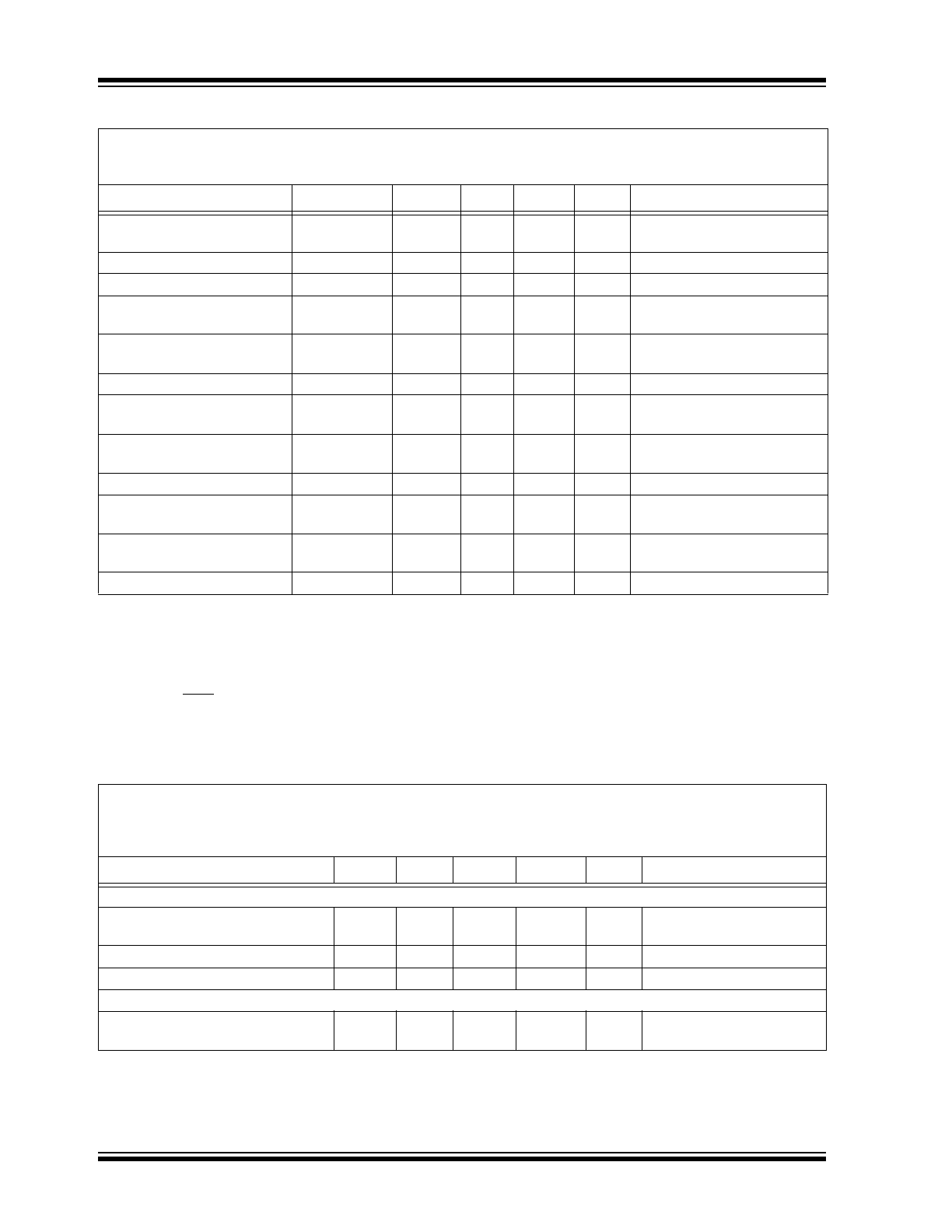
MCP1665
DS20005872A-page 4
2017 Microchip Technology Inc.
Load Regulation
|
V
FB
/V
FB
|
—
0.2
—
%
I
OUT
= 50 mA to 600 mA,
PWM only operation (
Note 4
)
Maximum Duty Cycle
DC
MAX
—
90
—
%
Note 4
Switching Frequency
f
SW
425
500
575
kHz
±15%
EN Input Logic High
V
IH
70
—
—
% of
V
IN
I
OUT
= 1 mA
EN Input Logic Low
V
IL
—
—
18
% of
V
IN
I
OUT
= 1 mA
EN Input Leakage Current
I
ENLK
—
5
—
nA
V
EN
= 5V
MODE Input Logic High
—
54
—
—
% of
V
IN
I
OUT
= 10 mA,
Note 4
MODE Input Logic Low
—
—
—
27
% of
V
IN
I
OUT
= 10 mA,
Note 4
MODE Input Leakage Current
—
—
5
—
nA
V
MODE
= 5V
Soft-Start Time
t
SS
—
3.7
—
ms
T
A
, EN Low-to-High,
90% of V
OUT
Thermal Shutdown
Die Temperature
T
SD
—
150
—
°C
Note 4
Die Temperature Hysteresis
T
SDHYS
—
15
—
°C
Note 4
TABLE 1-2:
TEMPERATURE SPECIFICATIONS
Electrical Specifications: Unless otherwise specified, all limits apply for typical values at ambient temperature
T
A
= +25°C, V
IN
= 3.6V, I
OUT
= 25 mA, V
OUT
= 12V, C
IN
= 22 µF, C
OUT
= 40 µF, X7R ceramic, L = 4.7 µH and 10-
Lead 2x2 mm VQFN package.
Boldface specifications apply over the controlled T
A
range of -40°C to +125°C.
Parameters
Sym.
Min.
Typ.
Max.
Units
Conditions
Temperature Ranges
Operating Junction Temperature
Range
T
J
–40
—
+125
°C
Steady State
Storage Temperature Range
T
A
–65
—
+150
°C
—
Maximum Junction Temperature
T
J
—
—
+150
°C
Transient
Package Thermal Resistances
Thermal Resistance, 10LD-VQFN-
2x2 mm
JA
—
48.3
—
°C/W
—
TABLE 1-1:
DC AND AC CHARACTERISTICS (CONTINUED)
Electrical Specifications: Unless otherwise specified, all limits apply for typical values at ambient temperature
T
A
= +25°C, V
IN
= 3.6V, I
OUT
= 25 mA, V
OUT
= 12V, C
IN
= 22 µF, C
OUT
= 40 µF, X7R ceramic, L = 4.7 µH.
Boldface specifications apply over the controlled T
A
range of –40°C to +125°C.
Parameters
Sym.
Min.
Typ.
Max.
Units
Conditions
Note 1: Minimum input voltage in the range of V
IN
(V
IN
≤ 5V < V
OUT
) depends on the maximum duty cycle
(DC
MAX
) and on the output voltage (V
OUT
), according to the boost converter equation:
V
INmin
= V
OUT
x (1 – DC
MAX
). (V
OUT
– V
IN
) > 1V is required for boost applications.
2: I
IN0
varies with input and output voltage and input capacitor leakage (
Figure 2-8
). I
IN0
is measured on the
V
IN
pin when the device is switching (EN = V
IN
), at no load, with R
TOP
= 180 k
and R
BOT
= 20 k
.
3: I
QSHDN
is measured on the V
IN
pin when the device is not switching (EN = GND), at no load, with the
feedback resistors (R
TOP
+ R
BOT
) disconnected from V
OUT
.
4: Determined by characterization, not production tested.
2017 Microchip Technology Inc.
DS20005872A-page 5
MCP1665
2.0
TYPICAL PERFORMANCE CURVES
Note: Unless otherwise specified, all limits apply for typical values at ambient temperature T
A
= +25°C, V
IN
= 3.6V,
I
OUT
= 25 mA, V
OUT
= 12V, C
IN
= 22 µF, C
OUT
= 40 µF, X7R ceramic, L = 4.7 µH and 10-Lead 2x2 mm VQFN package.
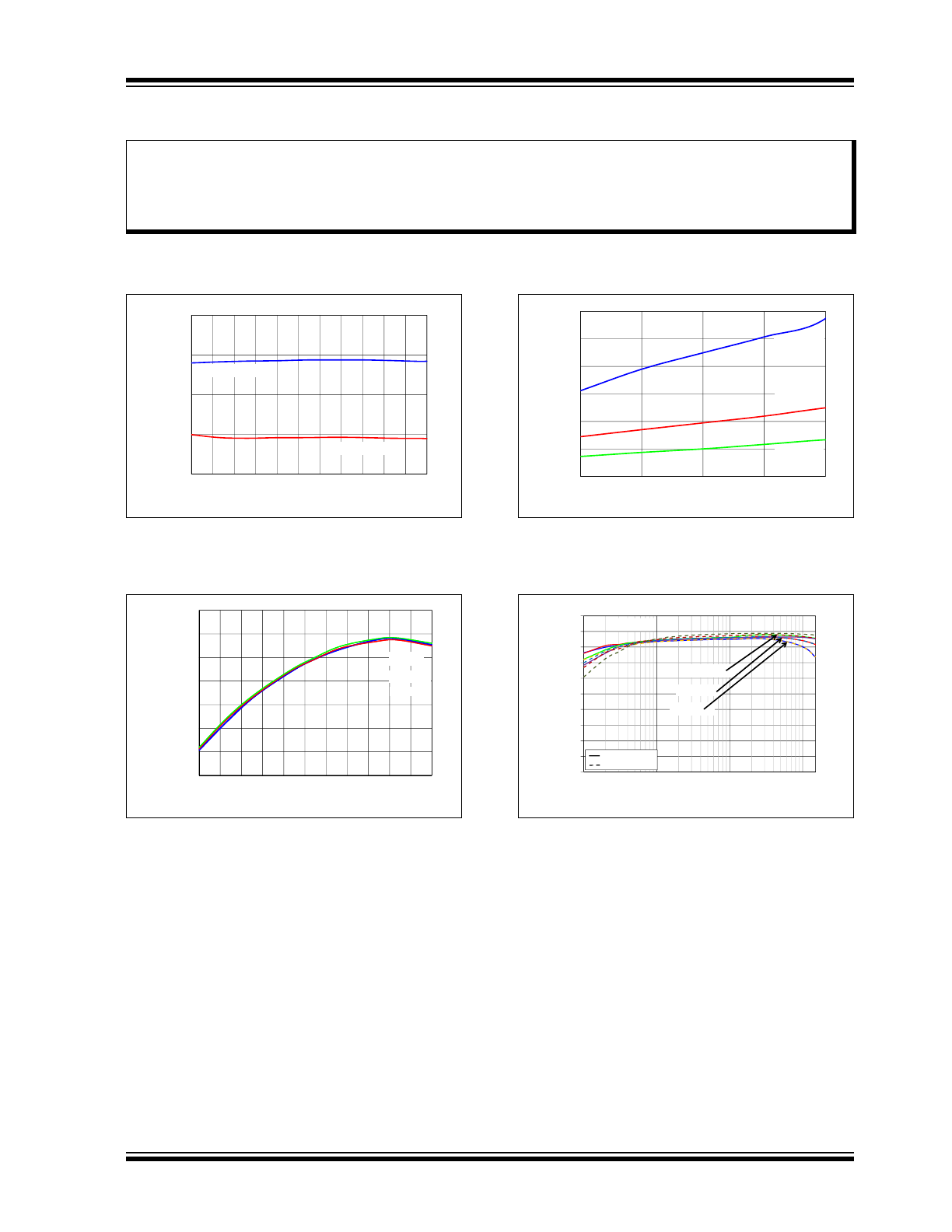
FIGURE 2-1:
Undervoltage Lockout
(UVLO) vs. Ambient Temperature.
FIGURE 2-2:
V
FB
Voltage vs. Ambient
Temperature and V
IN.
FIGURE 2-3:
Maximum Output Current
vs. V
IN
(V
OUT
in Regulation with Maximum 10%
Drop).
FIGURE 2-4:
6.0V V
OUT
Efficiency vs.
I
OUT
.
Note:
The graphs and tables provided following this note are a statistical summary based on a limited number of
samples and are provided for informational purposes only. The performance characteristics listed herein
are not tested or guaranteed. In some graphs or tables, the data presented may be outside the specified
operating range (for example, outside specified power supply range) and therefore outside the warranted
range.
2.6
2.7
2.8
2.9
3
-40 -25 -10
5
20
35
50
65
80
95 110 125
In
put V
o
lt
age (V)
Temperature (°C)
UVLO START
UVLO STOP
UVLO START
UVLO STOP
UVLO START
UVLO STOP
UVLO START
UVLO STOP
1.184
1.186
1.188
1.19
1.192
1.194
1.196
1.198
-40 -25 -10
5
20 35 50 65 80 95 110 125
Feed
back V
o
ltag
e (V)
Temperature (°C)
V
IN
=3V
V
IN
=5V
V
IN
=3.6V
0
0.5
1
1.5
2
2.5
3
3
3.5
4
4.5
5
I
OUT
(A)
V
IN
(V)
V
OUT
=24V
L=10uH
V
OUT
=12V
L=4.7uH
V
OUT
=6V
L=4.7uH
0
10
20
30
40
50
60
70
80
90
100
0.001
0.01
0.1
1
Eff
ici
ency (
%
)
I
OUT
(A)
V
OUT
=6V
V
IN
=3V
V
IN
=3.6V
PWM/PFM
PWM ONLY
V
IN
=4.5V
MCP1665
DS20005872A-page 6
2017 Microchip Technology Inc.
Note: Unless otherwise specified, all limits apply for typical values at ambient temperature T
A
= +25°C, V
IN
= 3.6V,
I
OUT
= 25 mA, V
OUT
= 12V, C
IN
= 22 µF, C
OUT
= 40 µF, X7R ceramic, L = 4.7 µH and 10-Lead 2x2 mm VQFN package.
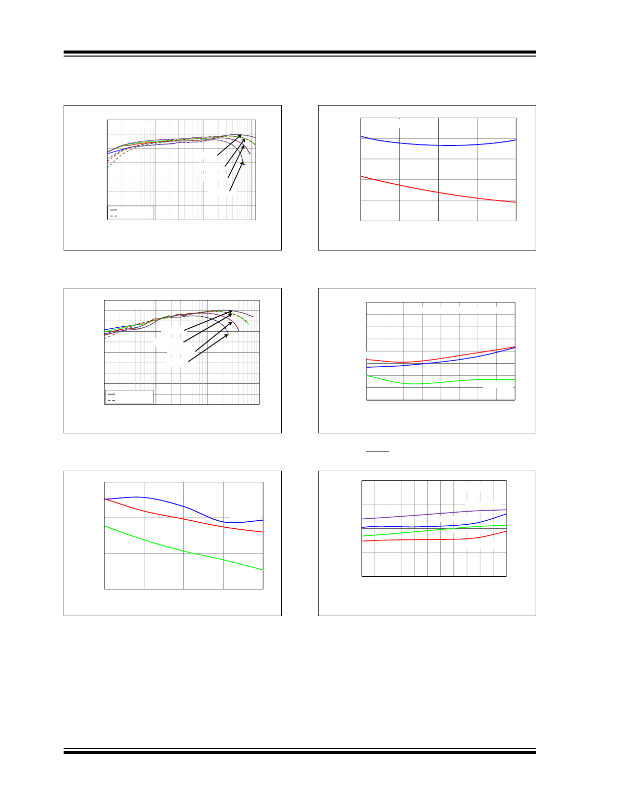
FIGURE 2-5:
12.0V V
OUT
Efficiency vs.
I
OUT
.
FIGURE 2-6:
24.0V V
OUT
Efficiency vs.
I
OUT
.
FIGURE 2-7:
Inductor Peak Current Limit
vs. Input Voltage.
FIGURE 2-8:
No Load Input Current, I
IN0
vs. V
IN
(EN = V
IN
).
FIGURE 2-9:
Shutdown Quiescent
Current,
I
QSHDN
vs. V
IN
(EN = GND).
FIGURE 2-10:
No Load Input Current,
I
IN0
vs. Ambient Temperature.
30
40
50
60
70
80
90
100
0.001
0.01
0.1
1
Eff
ici
ency (
%
)
I
OUT
(A)
V
OUT
=12V
V
IN
=3V
V
IN
=3.6V
PWM/PFM
PWM ONLY
V
IN
=4.5V
V
IN
=5V
0
10
20
30
40
50
60
70
80
90
100
0.001
0.01
0.1
1
Eff
ici
ency (
%
)
I
OUT
(A)
V
OUT
=24V
V
IN
=3V
V
IN
=3.6V
PWM/PFM
PWM ONLY
V
IN
=4.5V
V
IN
=5V
3.7
3.9
4.1
4.3
3
3.5
4
4.5
5
Inductor Peak
Current Limit (A)
V
IN
(V)
V
OUT
=24V
V
OUT
=12V
V
OUT
=6V
100
200
300
400
500
600
3
3.5
4
4.5
5
No Load Input Current (µA)
Input Voltage (V)
PFM/PWM
PWM only
V
OUT
=12V
0
0.1
0.2
0.3
0.4
0.5
0.6
0.7
0.8
3
3.25
3.5
3.75
4
4.25
4.5
4.75
5
I
Q
Shutdow
n
Current (µA)
V
IN
(V)
V
OUT
=12V
V
OUT
=24V
V
OUT
=6V
Note: Without FB Resistor Divider Current
0
125
250
375
500
-40 -25 -10
5
20
35
50
65
80
95 110 125
No
Load Input Current
(µA)
Temperature (°C)
PWM V
IN
=5V
PFM V
IN
=5V
PFM V
IN
=3.6V
PWM V
IN
=3.6V
V
OUT
=12V
2017 Microchip Technology Inc.
DS20005872A-page 7
MCP1665
Note: Unless otherwise specified, all limits apply for typical values at ambient temperature T
A
= +25°C, V
IN
= 3.6V,
I
OUT
= 25 mA, V
OUT
= 12V, C
IN
= 22 µF, C
OUT
= 40 µF, X7R ceramic, L = 4.7 µH and 10-Lead 2x2 mm VQFN package.
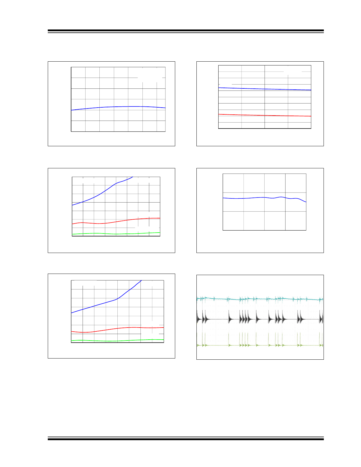
FIGURE 2-11:
f
SW
vs. Ambient
Temperature.
FIGURE 2-12:
PWM Pulse Skipping Mode
Threshold vs. V
IN
.
FIGURE 2-13:
PFM/PWM Mode Threshold.
FIGURE 2-14:
Enable Threshold vs. Input
Voltage.
FIGURE 2-15:
N-Channel Switch R
DSON
vs. V
IN
.
FIGURE 2-16:
12.0V V
OUT
Light Load
PWM Mode Waveforms.
425
450
475
500
525
550
575
-40
-15
10
35
60
85
110
Sw
itchin
g
F
requ
ency
(kHz)
Temperature (°C)
V
IN
=3.6V
V
OUT
=12V
I
OUT
=200 mA
0
20
40
60
80
100
120
140
3
3.25
3.5
3.75
4
4.25
4.5
4.75
5
I
OUT
(mA)
Input Voltage (V)
PWM Only
V
OUT
=6V
V
OUT
=12V
V
OUT
=24V
0
20
40
60
80
100
120
140
3
3.25
3.5
3.75
4
4.25
4.5
4.75
5
I
OUT
(mA
)
Input Voltage (V)
PFM/PWM
V
OUT
=12V
V
OUT
=6V
V
OUT
=24V
0
10
20
30
40
50
60
70
80
90
100
3
3.5
4
4.5
5
Enable Thresholds
(%
of V
IN
)
Input Voltage (V)
HIGH
LOW
V
OUT
=12V
I
OUT
=1mA
0
0.05
0.1
0.15
3
3.5
4
4.5
5
Sw
itch R
DSON
(:
)
Input Voltage (V)
I
OUT
= 5 mA
V
OUT
20 mV/div
AC Coupled 20 MHz BW
V
SW
5V/div
IL
200 mA/div
20 µs/div
MCP1665
DS20005872A-page 8
2017 Microchip Technology Inc.
Note: Unless otherwise specified, all limits apply for typical values at ambient temperature T
A
= +25°C, V
IN
= 3.6V,
I
OUT
= 25 mA, V
OUT
= 12V, C
IN
= 22 µF, C
OUT
= 40 µF, X7R ceramic, L = 4.7 µH and 10-Lead 2x2 mm VQFN package.
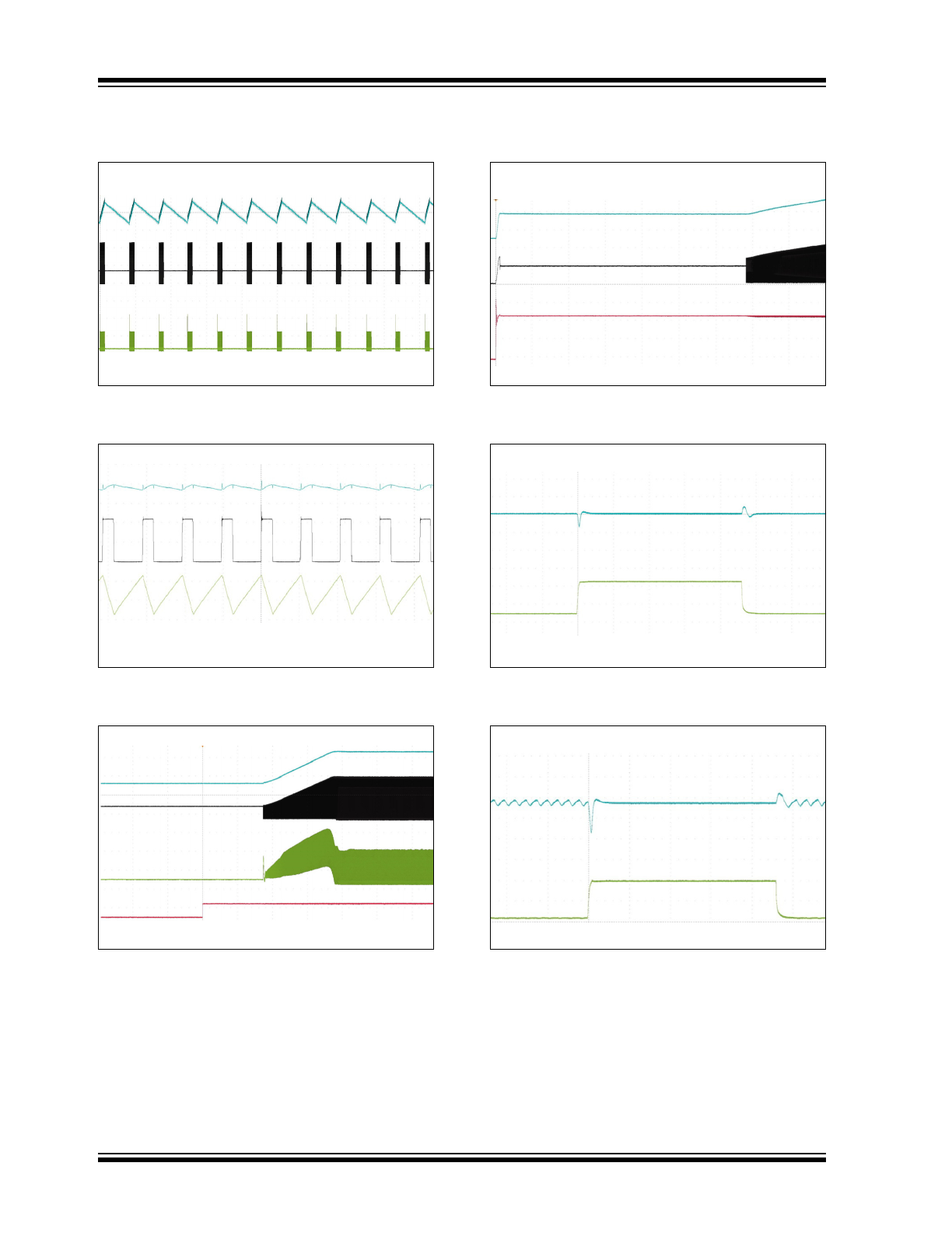
FIGURE 2-17:
12.0V V
OUT
Light Load
PFM Mode Waveforms.
FIGURE 2-18:
High-Load PWM Mode
Waveforms.
FIGURE 2-19:
12.0V Start-Up from Enable.
FIGURE 2-20:
12.0V Start-Up
(V
IN
= V
ENABLE
).
FIGURE 2-21:
12.0V V
OUT
Load Transient
Waveforms for PWM only (MODE = GND).
FIGURE 2-22:
12.0V V
OUT
Load Transient
Waveforms for PFM/PWM (MODE = V
IN
).
I
OUT
= 5 mA
1 ms/div
V
OUT
100 mV/div
AC Coupled 20 MHz BW
V
SW
5V/div
IL
500 mA/div
I
OUT
= 300 mA
V
OUT
50 mV/div
AC Coupled 20 MHz BW
V
SW
5V/div
IL
500 mA/div
2 µs/div
V
OUT
5V/div
V
SW
5V/div
IL
500 mA/div
V
EN
5V/div
1 ms/div
I
OUT
= 100 mA
400 µs/div
I
OUT
= 100 mA
V
OUT
5V/div
V
SW
5V/div
V
IN
2V/div
V
OUT
100 mV/div
AC Coupled 20 MHz BW
I
OUT
100 mA/div
I
OUT
20 to 200 mA
2 ms/div
V
IN
= 3.6V
V
IN
= 3.6V
2 ms/div
V
OUT
100 mV/div
AC Coupled 20 MHz BW
I
OUT
100 mA/div
I
OUT
20 to 200 mA
V
IN
= 3.6V
2017 Microchip Technology Inc.
DS20005872A-page 9
MCP1665
Note: Unless otherwise specified, all limits apply for typical values at ambient temperature T
A
= +25°C, V
IN
= 3.6V,
I
OUT
= 25 mA, V
OUT
= 12V, C
IN
= 22 µF, C
OUT
= 40 µF, X7R ceramic, L = 4.7 µH and 10-Lead 2x2 mm VQFN package.
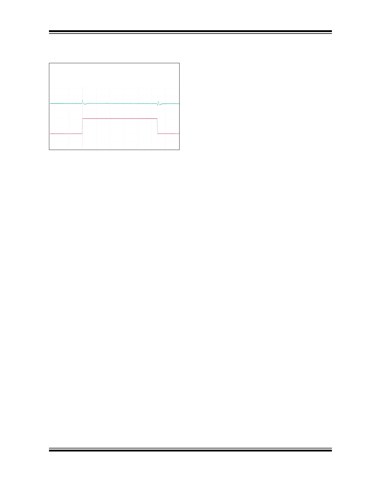
FIGURE 2-23:
12.0V V
OUT
Line Transient
Waveforms.
1 ms/div
V
IN
1V/div
V
IN
3V to 5V
V
OUT
50 mV/div
AC Coupled 20 MHz BW
I
OUT
= 100 mA

MCP1665
DS20005872A-page 10
2017 Microchip Technology Inc.
NOTES: