
2015 Microchip Technology Inc.
DS20005408A-page 1
MCP1664
Features
• 36V, 400 m
Integrated Switch
• Up to 92% Efficiency
• Drive LED Strings in Constant Current
• 1.8A Peak Input Current Limit:
- I
LED
up to 200 mA at 3.3V V
IN
, 4 White LEDs
- I
LED
up to 300 mA at 5.0V V
IN
, 4 White LEDs
- I
LED
up to 150 mA at 4.2V V
IN
, 8 White LEDs
• Input Voltage Range: 2.4V to 5.5V
• Undervoltage Lockout (UVLO):
- UVLO at V
IN
Rising: 2.3V, typical
- UVLO at V
IN
Falling: 1.85V, typical
• Shutdown Current (EN = GND): 40 nA Typical
• PWM Operation: 500 kHz Switching Frequency
• Cycle-by-Cycle Current Limiting
• Internal Compensation
• Open Load Protection (OLP) in the event of:
- Feedback Pin Shorted to GND (Prevent
Excessive Current into LEDs)
- Disconnected LED String (Prevent
Overvoltage to the Converter’s Output and
SW Pin)
• Overtemperature Protection
• Available Packages:
- 5-Lead SOT-23
- 8-Lead 2x3 TDFN
Applications
• Two and Three-Cell Alkaline or NiMH/NiCd White
LED Driver for Backlighting Products
• Li-Ion Battery LED Lightning Application
• Camera Flash
• LED Flashlights and Backlight Current Source
• Medical Equipment
• Portable Devices:
- Hand-Held Gaming Devices
- GPS Navigation Systems
- LCD Monitors
- Portable DVD Players
General Description
The MCP1664 is a compact, space-efficient,
fixed-frequency, non-synchronous step-up converter
optimized to drive multiple strings of LEDs with
constant current powered from two and three-cell
alkaline or NiMH/NiCd as well as from one-cell Li-Ion or
Li-Polymer batteries.
The device integrates a 36V, 400 m
low-side switch,
which is protected by the 1.8A cycle-by-cycle inductor
peak current limit operation. The MCP1664 starts up
without high inrush current or output overshoot. All
compensation and protection circuitry is integrated to
minimize the number of external components.
The internal feedback (V
FB
) voltage is set to 300 mV for
low power dissipation when sensing and regulating the
LED current. A single resistor sets the LED current.
The device features an UVLO which avoids start-up
with low inputs or discharged batteries for two
cell-powered applications.
The MCP1664 features an open load protection (OLP)
which turns off the operation in situations when the
LED string is accidentally disconnected or the feedback
pin is short-circuited to GND.
While in Shutdown mode (EN = GND), the device stops
switching, and consumes 40 nA typical of input current.
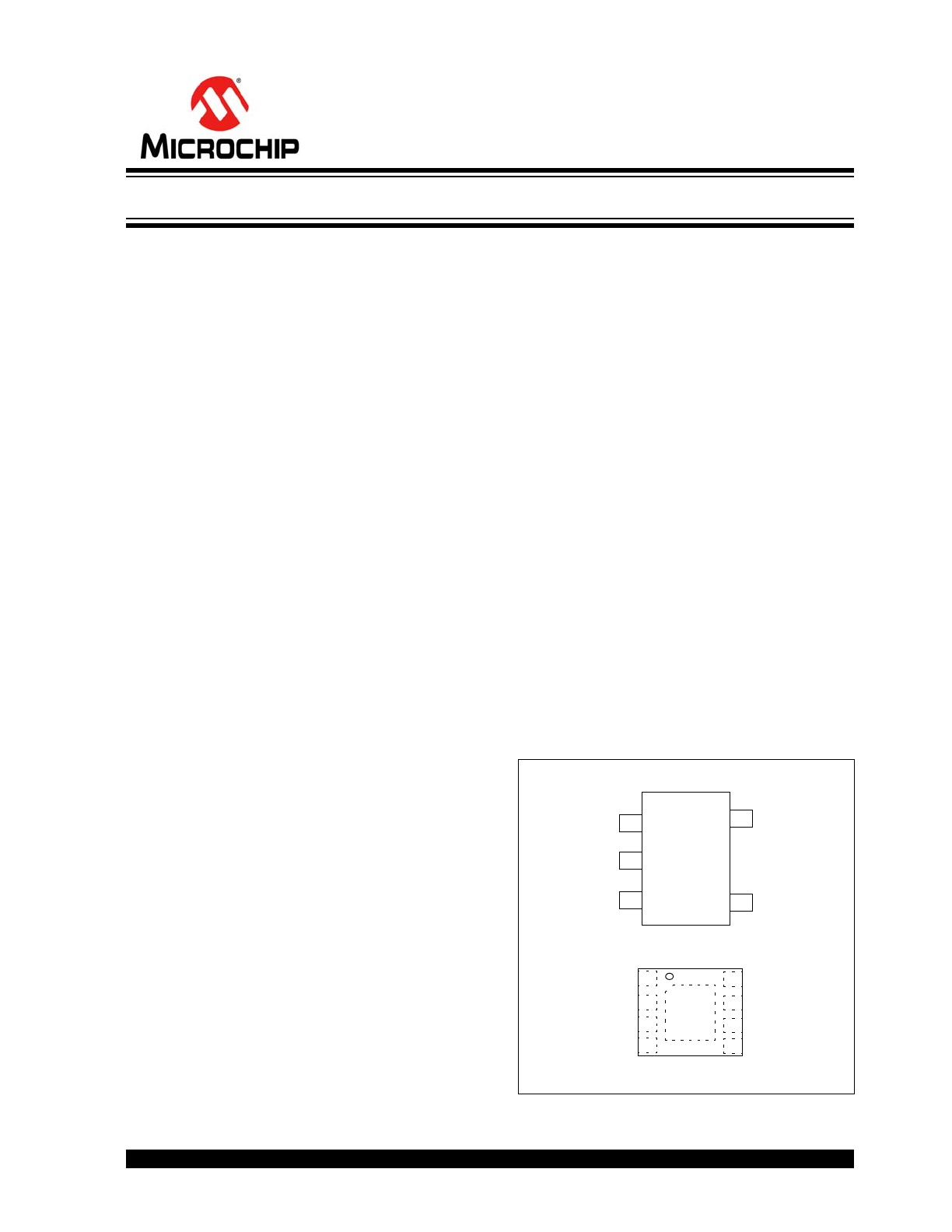
Package Types
* Includes Exposed Thermal Pad (EP); see
Table 3-1
.
SW
EN
V
IN
1
GND 2
P
GND
V
IN
NC
EN
V
FB
S
GND
SW
NC
MCP1664 SOT-23
V
FB
3
4
5
MCP1664 2x3 TDFN*
1
2
3
4
8
7
6
5
EP
9
High-Voltage Step-Up LED Driver with UVLO and Open Load Protection
MCP1664
DS20005408A-page 2
2015 Microchip Technology Inc.
Typical Application
V
IN
GND
V
FB
C
OUT
10 µF
C
IN
4.7 – 30 µF
L
4.7 – 10 µH
SW
EN
+
-
ALKAL
INE
ON
OFF
+
-
ALAKL
INE
V
IN
2.4V – 3.0V
LED6
12
R
SET
LED1
I
LED
= 25 mA
I
LED
=
0.3V
R
SET
LED2
Max. 32V
V
FB
= 0.3V
V
OUT
0
50
100
150
200
250
300
350
2
2.5
3
3.5
4
4.5
5
5.5
I
OUT
(mA)
V
IN
(V)
4 wLEDs, L = 4.7 µH
8 wLEDs, L = 10 µH
L = 4.7 µH for maximum 4 white LEDs
L = 10 µH for 5 to 10 white LEDs
C
IN
= 4.7 – 10 µF for V
IN
> 2.5V
C
IN
= 20 – 30 µF for V
IN
< 2.5V
D
MBRM140
MCP1664
Maximum LED Current in Regulation vs. Input Voltage, T
A
= +25°C
2015 Microchip Technology Inc.
DS20005408A-page 3
MCP1664
1.0
ELECTRICAL
CHARACTERISTICS
Absolute Maximum Ratings †
V
SW
– GND .....................................................................+36V
EN, V
IN
– GND ...............................................................+6.0V
V
FB
...............................................................................+0.35V
Power Dissipation ....................................... Internally Limited
Storage Temperature ....................................-65°C to +150°C
Ambient Temperature with Power Applied ....-40°C to +125°C
Operating Junction Temperature...................-40°C to +150°C
ESD Protection On All Pins:
HBM ................................................................. 4 kV
MM ..................................................................400V
† Notice: Stresses above those listed under “Maximum
Ratings” may cause permanent damage to the device.
This is a stress rating only and functional operation of
the device at those or any other conditions above those
indicated in the operational sections of this
specification is not intended. Exposure to maximum
rating conditions for extended periods may affect
device reliability.
DC AND AC CHARACTERISTICS
Electrical Specifications: Unless otherwise specified, all limits apply for typical values at ambient temperature
T
A
= +25°C, V
IN
= 3.3V, V
OUT
loaded with 3 white LEDs (V
F
= 2.65V at I
F
= 100 mA), I
LED
= 20 mA,
C
IN
= C
OUT
= 10 µF, X7R ceramic, L = 4.7 µH.
Boldface specifications apply over the controlled T
A
range of -40°C to +125°C.
Parameters
Sym.
Min.
Typ.
Max.
Units
Conditions
Input Voltage Range
V
IN
2.4
—
5.5
V
Note 1
Undervoltage Lockout (UVLO)
UVLO
START
—
2.3
—
V
V
IN
rising, I
LED
= 20 mA
UVLO
STOP
—
1.85
—
V
V
IN
falling, I
LED
= 20 mA
Maximum Output Voltage
V
OUTmax
—
—
32
V
Note 1
Maximum Output Current
I
OUT
—
150
—
mA
4.2V V
IN
, 8 LEDs
200
—
mA
3.3V V
IN
, 4 LEDs
300
—
mA
5.0V V
IN
, 4 LEDs
Feedback Voltage Reference
V
FB
275
300
325
mV
Feedback Input Bias Current
I
VFB
—
0.025
—
µA
Shutdown Quiescent Current
I
QSHDN
—
0.04
—
µA
EN = GND
NMOS Peak Switch Current
Limit
I
N(MAX)
—
1.8
—
A
Note 2
NMOS Switch Leakage
I
NLK
—
0.4
—
µA
V
IN
= V
SW
= 5V;
V
OUT
= 5.5V
V
EN
= V
FB
= GND
NMOS Switch ON Resistance
R
DS(ON)
—
0.4
—
V
IN
= 5V,
I
LED
= 100 mA,
4 series white LEDs
Note 2
Feedback Voltage Line
Regulation
|(
V
FB
/V
FB
)/
V
IN
|
—
0.5
1
%/V
V
IN
= 3.3V to 5V
Maximum Duty Cycle
DC
MAX
—
90
—
%
Note 2
Switching Frequency
f
SW
425
500
575
kHz
±15%
EN Input Logic High
V
IH
85
—
—
% of V
IN
EN Input Logic Low
V
IL
—
—
7.5
% of V
IN
EN Input Leakage Current
I
ENLK
—
0.025
—
µA
V
EN
= 5V
Note 1:
Minimum input voltage in the range of V
IN
(V
IN
< 5.5V < V
OUT
) depends on the maximum duty cycle
(DC
MAX
) and on the output voltage (V
OUT
), according to the boost converter equation:
V
INmin
= V
OUT
x (1 – DC
MAX
). Output voltage is equal to the LED voltage plus the voltage on the sense
resistor (V
LED
+ V_R
SET
). Recommended (V
OUT
- V
IN
) > 1V.
2:
Determined by characterization, not production tested.
MCP1664
DS20005408A-page 4
2015 Microchip Technology Inc.
Start-Up Time
t
SS
—
100
—
s
EN Low to High,
90% of I
LED
(
Note 2
,
Figure 2-10
)
Thermal Shutdown Die
Temperature
T
SD
—
150
—
°C
Note 2
Die Temperature Hysteresis
T
SDHYS
—
20
—
°C
Note 2
TEMPERATURE SPECIFICATIONS
Electrical Specifications: Unless otherwise specified, all limits apply for typical values at ambient temperature
T
A
= +25°C, V
IN
= 3.0V, I
OUT
= 20 mA, V
OUT
= 12V, C
IN
= C
OUT
= 10 µF, X7R ceramic, L = 4.7 µH.
Boldface specifications apply over the air-forced T
A
range of -40°C to +125°C.
Parameters
Sym.
Min.
Typ.
Max.
Units
Conditions
Temperature Ranges
Operating Junction Temperature
Range
T
J
-40
—
+125
°C
Steady State
Storage Temperature Range
T
A
-65
—
+150
°C
Maximum Junction Temperature
T
J
—
—
+150
°C
Package Thermal Resistances
Thermal Resistance, 5L SOT-23
JA
—
201.0
—
°C/W
Thermal Resistance, 8L 2x3 TDFN
JA
—
52.5
—
°C/W
DC AND AC CHARACTERISTICS (CONTINUED)
Electrical Specifications: Unless otherwise specified, all limits apply for typical values at ambient temperature
T
A
= +25°C, V
IN
= 3.3V, V
OUT
loaded with 3 white LEDs (V
F
= 2.65V at I
F
= 100 mA), I
LED
= 20 mA,
C
IN
= C
OUT
= 10 µF, X7R ceramic, L = 4.7 µH.
Boldface specifications apply over the controlled T
A
range of -40°C to +125°C.
Parameters
Sym.
Min.
Typ.
Max.
Units
Conditions
Note 1:
Minimum input voltage in the range of V
IN
(V
IN
< 5.5V < V
OUT
) depends on the maximum duty cycle
(DC
MAX
) and on the output voltage (V
OUT
), according to the boost converter equation:
V
INmin
= V
OUT
x (1 – DC
MAX
). Output voltage is equal to the LED voltage plus the voltage on the sense
resistor (V
LED
+ V_R
SET
). Recommended (V
OUT
- V
IN
) > 1V.
2:
Determined by characterization, not production tested.
2015 Microchip Technology Inc.
DS20005408A-page 5
MCP1664
2.0
TYPICAL PERFORMANCE CURVES
Note: Unless otherwise indicated: V
IN
= 3.3V, I
LED
= 20 mA, V
OUT
loaded with 4 white LEDs
(V
F
= 2.9V at I
F
= 100 mA), C
IN
= C
OUT
= 10 µF, X7R ceramic, L = 4.7 µH.
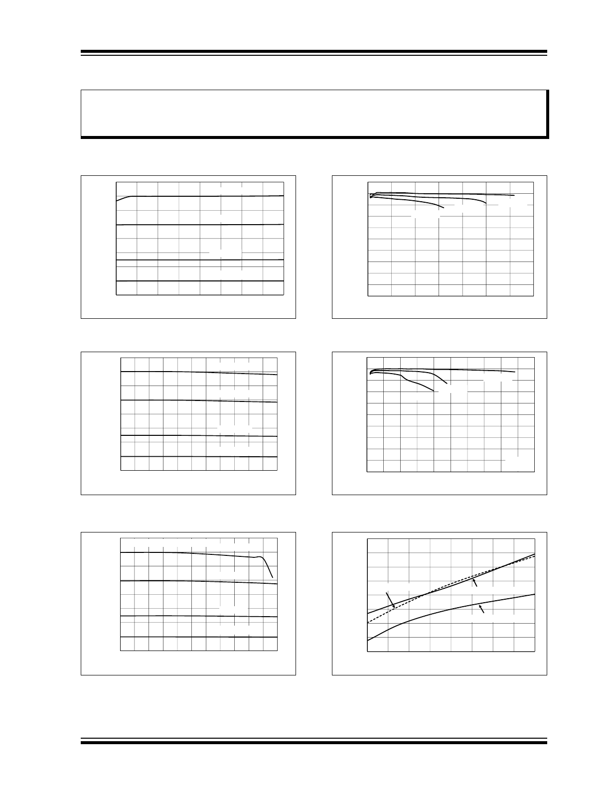
FIGURE 2-1:
Four White LEDs, I
LED
vs.
V
IN
.
FIGURE 2-2:
Four White LEDs, I
LED
vs.
Ambient Temperature.
FIGURE 2-3:
Eight White LEDs, I
LED
vs.
Ambient Temperature.
FIGURE 2-4:
Four White LEDs, Efficiency
vs. I
LED
.
FIGURE 2-5:
Eight White LEDs, Efficiency
vs. I
LED
.
FIGURE 2-6:
Maximum I
LED
vs. V
IN
.
Note:
The graphs and tables provided following this note are a statistical summary based on a limited number of
samples and are provided for informational purposes only. The performance characteristics listed herein
are not tested or guaranteed. In some graphs or tables, the data presented may be outside the specified
operating range (e.g., outside specified power supply range) and therefore outside the warranted range.
0
20
40
60
80
100
120
140
160
2.3
2.7
3.1
3.5
3.9
4.3
4.7
5.1
5.5
LED Current
(mA)
Input Voltage (V)
R
SET
= 15.2ȍ
R
SET
= 6ȍ
R
SET
= 2.1ȍ
R
SET
= 3ȍ
0
20
40
60
80
100
120
140
160
-40 -25 -10 5
20 35 50 65 80 95 110 125
LED Cur
rent
(mA)
Ambient Temperature (
o
C)
R
SET
= 15.2ȍ
R
SET
= 6ȍ
R
SET
= 3ȍ
R
SET
= 2.1ȍ
0
20
40
60
80
100
120
140
160
-40 -25 -10 5
20 35 50 65 80 95 110 125
LED Current (mA)
Ambient Temperature (
o
C)
R
SET
= 15.2ȍ
8 x wLED, L = 10μH, V
IN
= 4.2V
R
SET
= 6ȍ
R
SET
= 3ȍ
R
SET
= 2.1ȍ
0
10
20
30
40
50
60
70
80
90
100
0
50
100
150
200
250
300
350
Efficien
cy
(%
)
I
LED
(mA)
V
IN
= 3.0V
V
IN
= 4.0V
V
IN
= 5.5V
0
10
20
30
40
50
60
70
80
90
100
0
50
100
150
200
250
Eff
ici
ency (%
)
I
LED
(mA)
V
IN
= 4.0V
V
IN
= 5.5V
V
IN
= 3.0V
8 x wLED
L = 10 µH
0
50
100
150
200
250
300
350
400
2.3
2.7
3.1
3.5
3.9
4.3
4.7
5.1
5.5
LED Current
(m
A)
Input Voltage (V)
8 wLEDs, L = 10 µH
4 wLEDs, L = 4.7µH
5 wLEDs, L = 10µH
MCP1664
DS20005408A-page 6
2015 Microchip Technology Inc.
Note: Unless otherwise indicated: V
IN
= 3.3V, I
LED
= 20 mA, V
OUT
loaded with 4 white LEDs
(V
F
= 2.9V at I
F
= 100 mA), C
IN
= C
OUT
= 10 µF, X7R ceramic, L = 4.7 µH.
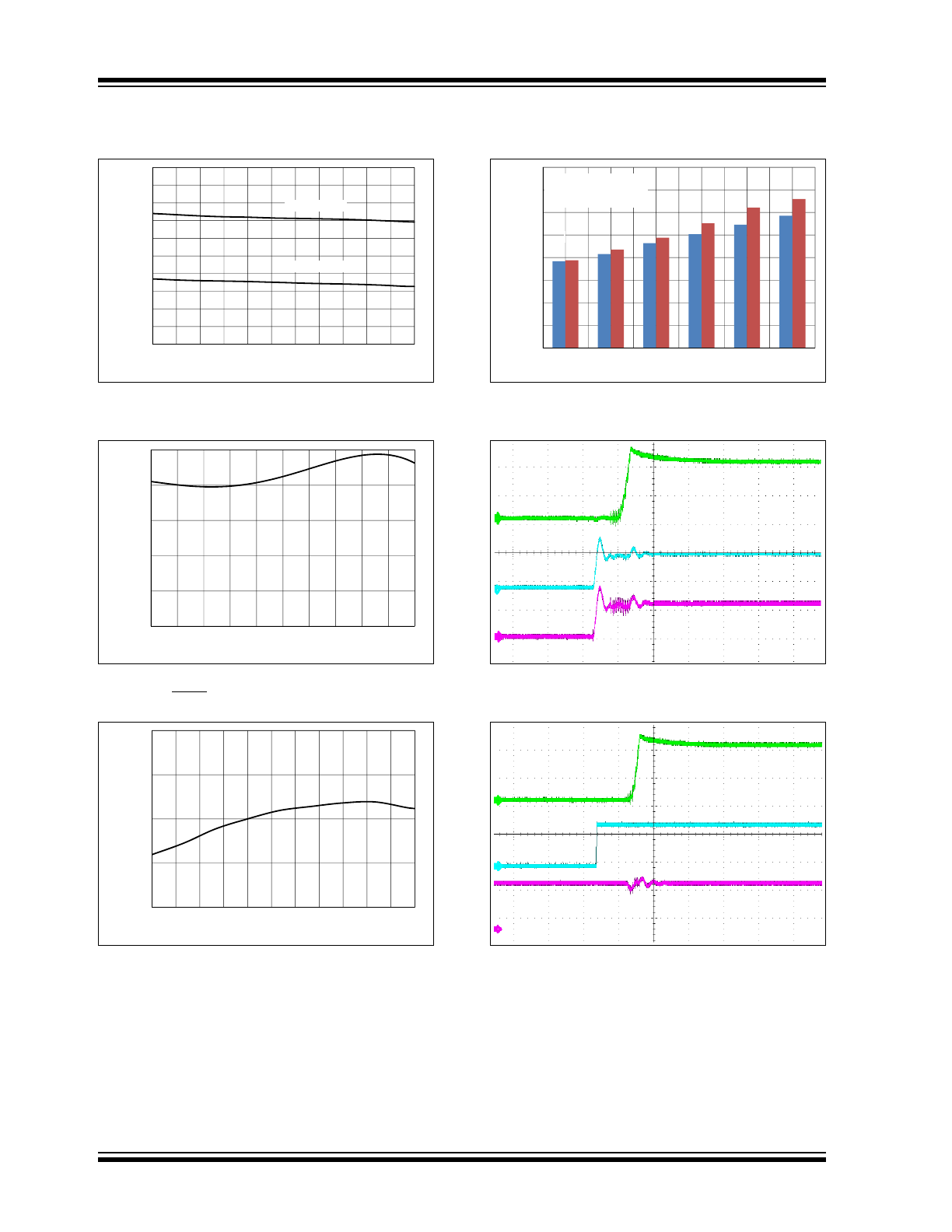
FIGURE 2-7:
Undervoltage Lockout
(UVLO) vs. Ambient Temperature.
FIGURE 2-8:
Shutdown Quiescent
Current,
I
QSHDN
, vs. V
IN
(EN = GND).
FIGURE 2-9:
Switching Frequency,
f
SW
vs. Ambient Temperature.
FIGURE 2-10:
Start-Up Time vs.
LED Number.
FIGURE 2-11:
Start-Up When
V
IN
= V
ENABLE
.
FIGURE 2-12:
Start-Up After Enable.
1.5
1.6
1.7
1.8
1.9
2
2.1
2.2
2.3
2.4
2.5
-40 -25 -10
5
20
35
50
65
80
95 110 125
UVLO Thresholds (V)
Ambient Temperature (
o
C)
UVLO Stop
UVLO Start
0
10
20
30
40
50
2.5 2.8 3.1 3.4 3.7 4.0 4.3 4.6 4.9 5.2 5.5
Shutdow
n I
Q
(nA)
Input Voltage (V)
450
475
500
525
550
-40 -25 -10
5
20
35
50
65
80
95 110 125
Sw
itching Frequency
(kHz)
Ambient Temperature (°C)
0
25
50
75
100
125
150
175
200
3
4
5
6
7
8
S
o
ft Sta
rt
T
ime
(µ
s)
Number of LEDs
Blue Bars: I
LED
= 20 mA
Red Bars: I
LED
= 40 mA
C
OUT
= 10 µF
I
LED
10 mA/div
EN
2V/div
V
IN
2V/div
80µs/div
3 wLEDs
I
LED
10 mA/div
EN
2V/div
V
IN
2V/div
80µs/div
3 wLEDs
2015 Microchip Technology Inc.
DS20005408A-page 7
MCP1664
Note: Unless otherwise indicated: V
IN
= 3.3V, I
LED
= 20 mA, V
OUT
loaded with 4 white LEDs
(V
F
= 2.9V at I
F
= 100 mA), C
IN
= C
OUT
= 10 µF, X7R ceramic, L = 4.7 µH.
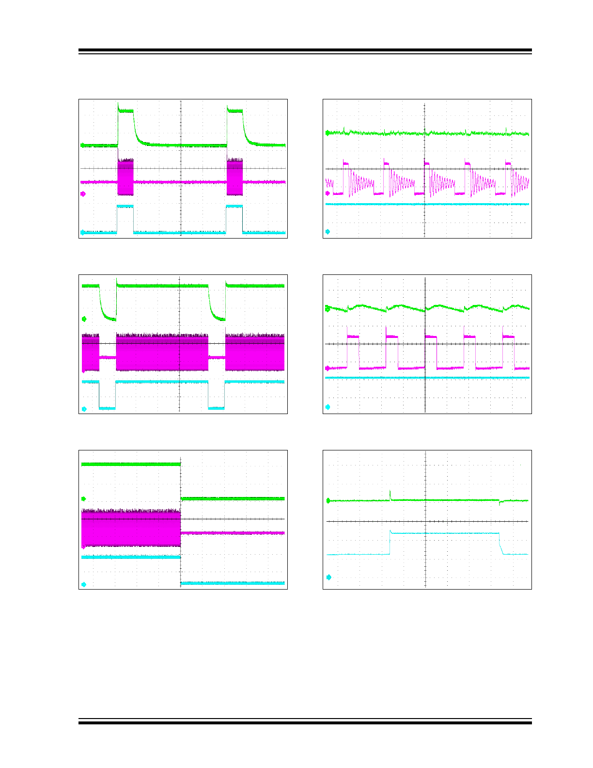
FIGURE 2-13:
100 Hz PWM Dimming,
15% Duty Cycle.
FIGURE 2-14:
100 Hz PWM Dimming,
85% Duty Cycle.
FIGURE 2-15:
Open Load (LED Fail or FB
to GND) Response.
FIGURE 2-16:
Three White LEDs PWM
Discontinuous Mode Waveforms.
FIGURE 2-17:
Three White LEDs PWM
Continuous Mode Waveforms.
FIGURE 2-18:
Line Step Response.
V
IN
steps from 2.5V to 4.5V.
I
LED
10 mA/div
SW
5V/div
EN
2V/div
2 ms/div
3 wLEDs
I
LED
10 mA/div
SW
5V/div
EN
2V/div
2 ms/div
3 wLEDs
I
LED
10 mA/div
SW
5V/div
V
FB
200mV/div
10 ms/div
3 wLEDs
I
LED
AC Coupled
SW
5V/div
V
OUT
5V/div
1 µs/div
3 wLEDs
2 mA/div
I
LED
= 20 mA
I
LED
AC Coupled
SW
5V/div
V
OUT
5V/div
1 µs/div
3 wLEDs
10 mA/div
I
LED
= 145 mA
I
LED
AC Coupled
V
IN
2V/div
1 ms/div
Line Step
2 mA/div
2.5V to 4.5V
3 wLEDs
I
LED
= 20mA
Step from 2.5V to 4.5V

MCP1664
DS20005408A-page 8
2015 Microchip Technology Inc.
NOTES:
2015 Microchip Technology Inc.
DS20005408A-page 9
MCP1664
3.0
PIN DESCRIPTIONS
The descriptions of the pins are listed in
Table 3-1
.
3.1
Feedback Voltage Pin (V
FB
)
The V
FB
pin is used to regulate the voltage across the
R
SET
sense resistor to 300 mV to keep the output LED
current in regulation. Connect the cathode of the LED
to the V
FB
pin.
3.2
Signal Ground Pin (S
GND
)
The signal ground pin is used as a return for the
integrated reference voltage and error amplifier.
3.3
Switch Node Pin (SW)
Connect the inductor from the input voltage to the SW
pin. The SW pin carries inductor current and has a
typical value of 1.8A. The integrated N-Channel switch
drain is internally connected to the SW node.
3.4
Not Connected (NC)
This is an unconnected pin.
3.5
Power Supply Input Voltage Pin
(V
IN
)
Connect the input voltage source to V
IN
. The input
source should be decoupled from GND with a 4.7 µF
minimum capacitor.
3.6
Power Ground Pin (P
GND
)
The power ground pin is used as a return for the
high-current N-Channel switch. The P
GND
and S
GND
pins are connected externally. The signal ground and
power ground must be connected externally in one
point.
3.7
Enable Pin (EN)
The EN pin is a logic-level input used to enable or
disable device switching and lower quiescent current
while disabled. A logic high (>85% of V
IN
) will enable
the regulator output. A logic low (<7.5% of V
IN
) will
ensure that the regulator is disabled.
3.8
Exposed Thermal Pad (EP)
There is no internal electrical connection between the
Exposed Thermal Pad (EP) and the S
GND
and P
GND
pins. They must be connected to the same potential on
the Printed Circuit Board (PCB).
3.9
Ground Pin (GND)
The ground or return pin is used for circuit ground
connection. The length of the trace from the input cap
return, the output cap return and the GND pin must be
as short as possible to minimize noise on the GND pin.
The SOT-23 5-lead package uses a single ground pin.
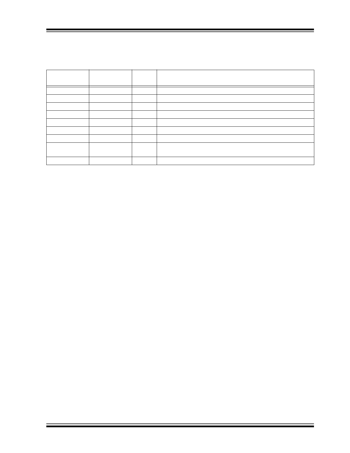
TABLE 3-1:
PIN FUNCTION TABLE
MCP1664
SOT-23
MCP1664
2x3 TDFN
Symbol
Description
3
1
V
FB
Feedback Voltage Pin
—
2
S
GND
Signal Ground Pin (TDFN only)
1
3
SW
Switch Node, Boost Inductor Pin
—
4, 6
NC
Not Connected
5
5
V
IN
Input Voltage Pin
—
7
P
GND
Power Ground Pin (TDFN only)
4
8
EN
Enable Control Input Pin
—
9
EP
Exposed Thermal Pad (EP); must be connected to Ground.
(TDFN only)
2
—
GND
Ground Pin (SOT-23 only)

MCP1664
DS20005408A-page 10
2015 Microchip Technology Inc.
NOTES: