
2015 Microchip Technology Inc.
DS20005406A-page 1
MCP1663
Features
• 36V, 400 mΩ Integrated Switch
• Up to 92% Efficiency
• Output Voltage Range: up to 32V
• 1.8A Peak Input Current Limit:
- I
OUT
> 375 mA @ 5.0V V
IN
, 12V V
OUT
- I
OUT
> 200 mA @ 3.3V V
IN
, 12V V
OUT
- I
OUT
> 150 mA @ 4.2V V
IN
, 24V V
OUT
• Input Voltage Range: 2.4V to 5.5V
• Undervoltage Lockout (UVLO):
- UVLO @ V
IN
Rising: 2.3V, typical
- UVLO @ V
IN
Falling: 1.85V, typical
• No Load Input Current: 250 µA, typical
• Sleep mode with 0.3 µA Typical Shutdown
Quiescent Current
• PWM Operation with Skip Mode: 500 kHz
• Feedback Voltage Reference: V
FB
= 1.227V
• Cycle-by-Cycle Current Limiting
• Internal Compensation
• Inrush Current Limiting and Internal Soft Start
• Output Overvoltage Protection (OVP) in the event
of:
- Feedback pin shorted to GND
- Disconnected feedback divider
• Overtemperature Protection
• Easily Configurable for SEPIC, Cuk or Flyback
Topologies
• Available Packages:
- 5-Lead SOT-23
- 8-Lead 2x3 TDFN
Applications
• Two and Three-Cell Alkaline, Lithium Ultimate and
NiMH/NiCd Portable Products
• Single-Cell Li-Ion to 5V, 12V or 24V Converters
• LCD Bias Supply for Portable Applications
• Camera Phone Flash
• Portable Medical Equipment
• Hand-Held Instruments
General Description
The MCP1663 device is a compact, high-efficiency,
fixed-frequency, non-synchronous step-up DC-DC
converter which integrates a 36V, 400 mΩ NMOS
switch. It provides a space-efficient high-voltage
step-up power supply solution for applications powered
by either two-cell or three-cell alkaline, Ultimate
Lithium, NiCd, NiMH, one-cell Li-Ion or Li-Polymer
batteries.
The integrated switch is protected by the 1.8A
cycle-by-cycle inductor peak current limit operation.
There is an output overvoltage protection which turns
off switching in case the feedback resistors are
accidentally disconnected or the feedback pin is
short-circuited to GND.
Low-voltage technology allows the regulator to start-up
without high inrush current or output voltage overshoot
from a low-voltage input. The device features a UVLO
which avoids start-up and operation with low inputs or
discharged batteries for two cell-powered applications.
For standby applications (EN = GND), the device stops
switching, enters sleep mode and consumes 0.3 µA
(typical) of input current.
MCP1663 is easy to use and allows creating classic
boost, SEPIC or flyback DC-DC converters within a
small Printed Circuit Board (PCB) area. All
compensation and protection circuitry is integrated to
minimize the number of external components. Ceramic
input and output capacitors are used.
Package Types
* Includes Exposed Thermal Pad (EP); see
Table 3-1
.
SW
EN
V
IN
GND
MCP1663
SOT-23
V
FB
MCP1663
2x3 TDFN*
1
2
3
5
4
SW
S
GND
NC
P
GND
NC
1
2
3
4
8
7
6
5 V
IN
EN
V
FB
EP
9
High-Voltage Integrated Switch PWM Boost Regulator with UVLO
MCP1663
DS20005406A-page 2
2015 Microchip Technology Inc.
Typical Applications
Maximum Output Current vs. Input Voltage
V
IN
GND
V
FB
V
OUT
12V, 250 mA
C
OUT
4.7 - 10 µF
C
IN
4.7 - 10 µF
L
4.7 µH
SW
1.05 MΩ
120 Ω
EN
+
-
1 X LI-ION
ON
OFF
MCP1663
R
TOP
R
BOT
V
IN
3.6V to 4.5V
D
PMEG2010
3 X ALKALINE
OR
BAT
T
E
RY
V
IN
GND
V
FB
V
OUT
24V, 100 mA
C
OUT
10 - 22 µF
C
IN
10 µF
L
10 µH
SW
1.05 MΩ
56 Ω
EN
+
-
BA
T
T
E
R
Y
MCP1663
R
TOP
R
BOT
V
IN
3.6V to 4.5V
D
MBRM140
1 X LI-ION
3 X ALKALINE
OR
ON
OFF
0
50
100
150
200
250
300
350
400
450
2.4 2.7
3
3.3 3.6 3.9 4.2 4.5 4.8 5.1 5.4
I
OUT
(mA)
V
IN
(V)
V
OUT
= 12V
V
OUT
= 24V
k
k
2015 Microchip Technology Inc.
DS20005406A-page 3
MCP1663
1.0
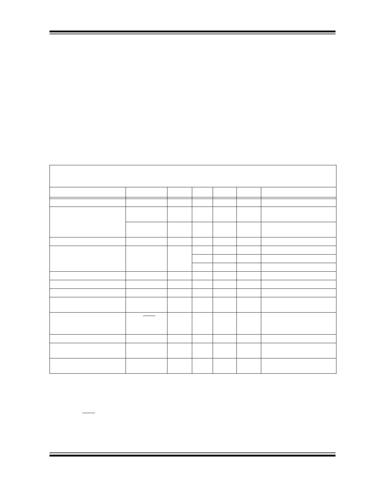
ELECTRICAL
CHARACTERISTICS
Absolute Maximum Ratings †
V
SW
– GND .....................................................................+36V
EN, V
IN
– GND...............................................................+6.0V
V
FB
.................................................................................+1.3V
Power Dissipation ....................................... Internally Limited
Storage Temperature ....................................-65°C to +150°C
Ambient Temperature with Power Applied ....-40°C to +125°C
Operating Junction Temperature...................-40°C to +150°C
ESD Protection On All Pins:
HBM ................................................................. 4 kV
MM ..................................................................400V
† Notice: Stresses above those listed under “Maximum
Ratings” may cause permanent damage to the device.
This is a stress rating only and functional operation of
the device at those or any other conditions above those
indicated in the operational sections of this
specification is not intended. Exposure to maximum
rating conditions for extended periods may affect
device reliability.
DC AND AC CHARACTERISTICS
Electrical Specifications:
Unless otherwise specified, all limits apply for typical values at ambient temperature
T
A
= +25°C, V
IN
= 3.3V, I
OUT
= 20 mA, V
OUT
= 12V, C
IN
= C
OUT
= 10 µF, X7R ceramic, L = 4.7 µH.
Boldface
specifications apply over the controlled T
A
range of -40°C to +125°C.
Parameters
Sym.
Min.
Typ.
Max.
Units
Conditions
Input Voltage Range
V
IN
2.4
—
5.5
V
Note 1
Undervoltage Lockout
(UVLO)
UVLO
START
—
2.3
—
V
V
IN
rising,
I
OUT
= 1 mA resistive load
UVLO
STOP
—
1.85
—
V
V
IN
falling,
I
OUT
= 1 mA resistive load
Output Voltage Adjust Range
V
OUT
—
—
32
V
Note 1
Maximum Output Current
I
OUT
—
200
—
mA
3.3V V
IN
, 12V V
OUT
(
Note 4
)
375
—
mA
5.0V V
IN
, 12V V
OUT
(
Note 4
)
150
—
mA
4.2V V
IN
, 24V V
OUT
(
Note 4
)
Feedback Voltage
V
FB
1.190
1.227
1.264
V
V
FB
Accuracy
-3
—
3
%
Feedback Input Bias Current
I
VFB
—
0.025
—
µA
No Load Input Current
I
IN0
—
250
—
µA
Device switching, no load,
3.3V V
IN
, 12V V
OUT
(
Note 2
)
Shutdown Quiescent Current
I
QSHDN
—
300
—
nA
EN = GND,
feedback divider current not
included (
Note 3
)
Peak Switch Current Limit
I
Lmax
—
1.8
—
A
Note 4
NMOS Switch Leakage
I
NLK
—
0.4
—
µA
V
IN
= V
SW
= 5V; V
OUT
= 5.5V
V
EN
= V
FB
= GND
NMOS Switch ON Resistance
R
DS(ON)
—
0.4
—
Ω
V
IN
= 5V, V
OUT
= 12V,
I
OUT
= 100 mA (
Note 4
)
Note 1:
Minimum input voltage in the range of V
IN
(V
IN
≤ 5.5V < V
OUT
) depends on the maximum duty cycle
(DC
MAX
) and on the output voltage (V
OUT
), according to the boost converter equation:
V
INmin
= V
OUT
x (1 – DC
MAX
). Recommended (V
OUT
- V
IN
) > 1V for boost applications.
2:
I
IN0
varies with input and output voltage (
Figure 2-8
). I
IN0
is measured on the V
IN
pin when the device is
switching (EN = V
IN
), at no load, with R
TOP
= 120 k
and R
BOT
= 1.05 MΩ.
3:
I
QSHDN
is measured on the V
IN
pin when the device is not switching (EN = GND), at no load, with the
feedback resistors (R
TOP
+ R
BOT
) disconnected from V
OUT
.
4:
Determined by characterization, not production tested.
MCP1663
DS20005406A-page 4
2015 Microchip Technology Inc.
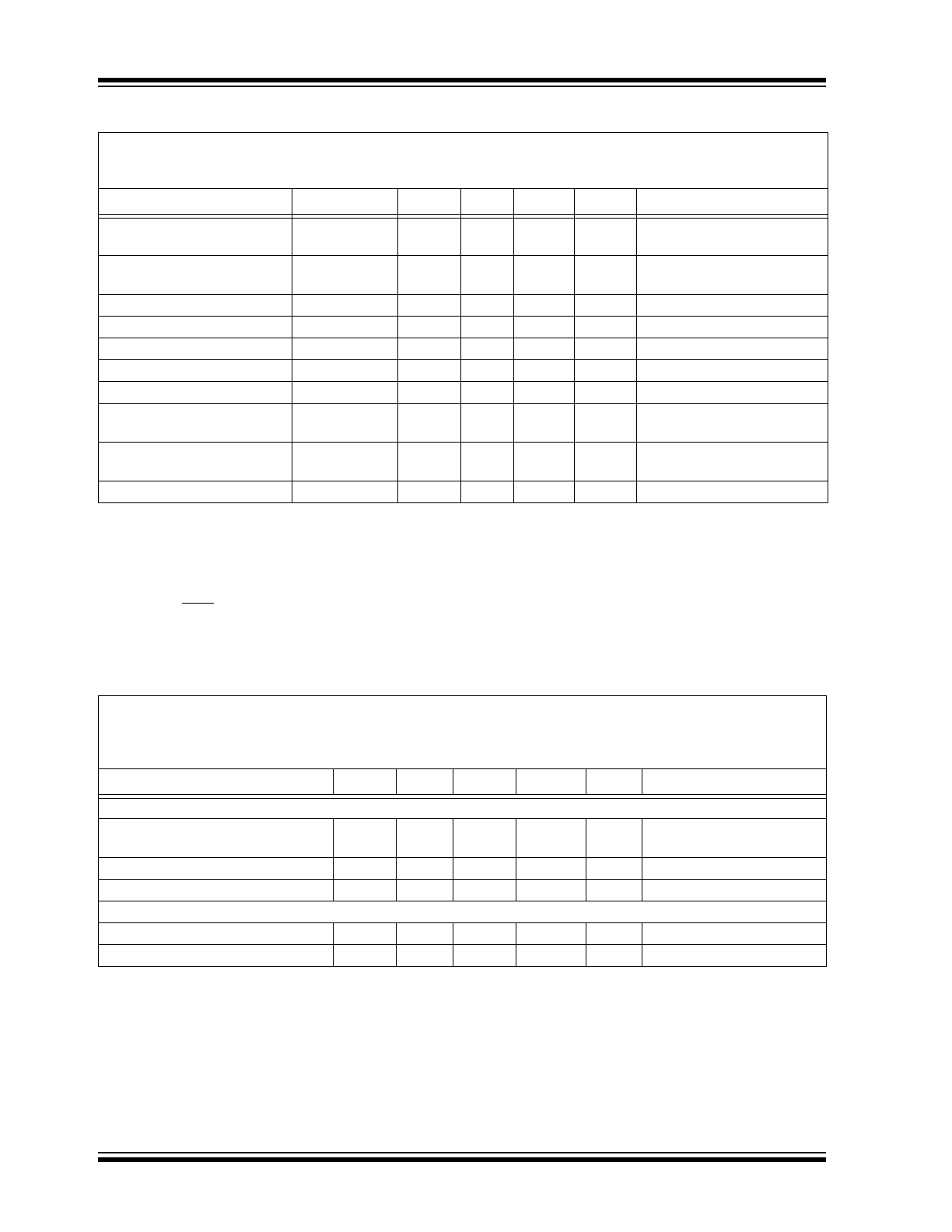
Line Regulation
|(
V
FB
/V
FB
)/
V
IN
|
—
0.05
0.5
%/V
V
IN
= 3V to 5V,
I
OUT
= 20 mA, V
OUT
= 12.0V
Load Regulation
|
V
FB
/V
FB
|
—
0.5
1.5
%
I
OUT
= 20 mA to 125 mA,
V
IN
= 3.3V, V
OUT
= 12.0V
Maximum Duty Cycle
DC
MAX
88
90
—
%
Note 4
Switching Frequency
f
SW
425
500
575
kHz
±15%
EN Input Logic High
V
IH
85
—
—
% of V
IN
I
OUT
= 1 mA
EN Input Logic Low
V
IL
—
—
7.5
% of V
IN
I
OUT
= 1 mA
EN Input Leakage Current
I
ENLK
—
0.025
—
µA
V
EN
= 5V
Soft-Start Time
t
SS
—
3
—
ms
T
A
, EN Low-to-High,
90% of V
OUT
Thermal Shutdown
Die Temperature
T
SD
—
150
—
°C
Die Temperature Hysteresis
T
SDHYS
—
15
—
°C
TEMPERATURE SPECIFICATIONS
Electrical Specifications:
Unless otherwise specified, all limits apply for typical values at ambient temperature
T
A
= +25°C, V
IN
= 3.3V, I
OUT
= 20 mA, V
OUT
= 12V, C
IN
= C
OUT
= 10 µF, X7R ceramic, L = 4.7 µH and 5-lead
SOT-23 package.
Boldface
specifications apply over the controlled T
A
range of -40°C to +125°C.
Parameters
Sym.
Min.
Typ.
Max.
Units
Conditions
Temperature Ranges
Operating Junction Temperature
Range
T
J
-40
—
+125
°C
Steady State
Storage Temperature Range
T
A
-65
—
+150
°C
Maximum Junction Temperature
T
J
—
—
+150
°C
Transient
Package Thermal Resistances
Thermal Resistance, 5LD-SOT-23
JA
—
201.0
—
°C/W
Thermal Resistance, 8LD-2x3 TDFN
JA
—
52.5
—
°C/W
DC AND AC CHARACTERISTICS (CONTINUED)
Electrical Specifications:
Unless otherwise specified, all limits apply for typical values at ambient temperature
T
A
= +25°C, V
IN
= 3.3V, I
OUT
= 20 mA, V
OUT
= 12V, C
IN
= C
OUT
= 10 µF, X7R ceramic, L = 4.7 µH.
Boldface
specifications apply over the controlled T
A
range of -40°C to +125°C.
Parameters
Sym.
Min.
Typ.
Max.
Units
Conditions
Note 1:
Minimum input voltage in the range of V
IN
(V
IN
≤ 5.5V < V
OUT
) depends on the maximum duty cycle
(DC
MAX
) and on the output voltage (V
OUT
), according to the boost converter equation:
V
INmin
= V
OUT
x (1 – DC
MAX
). Recommended (V
OUT
- V
IN
) > 1V for boost applications.
2:
I
IN0
varies with input and output voltage (
Figure 2-8
). I
IN0
is measured on the V
IN
pin when the device is
switching (EN = V
IN
), at no load, with R
TOP
= 120 k
and R
BOT
= 1.05 MΩ.
3:
I
QSHDN
is measured on the V
IN
pin when the device is not switching (EN = GND), at no load, with the
feedback resistors (R
TOP
+ R
BOT
) disconnected from V
OUT
.
4:
Determined by characterization, not production tested.
2015 Microchip Technology Inc.
DS20005406A-page 5
MCP1663
2.0
TYPICAL PERFORMANCE CURVES
Note:
Unless otherwise indicated, V
IN
= 3.3V, I
OUT
= 20 mA, V
OUT
= 12V, C
IN
= C
OUT
= 10 µF, X7R ceramic,
L = 4.7 µH, R
TOP
= 120 kΩ and R
BOT
= 1.05 MΩ, T
A
= 25°C.
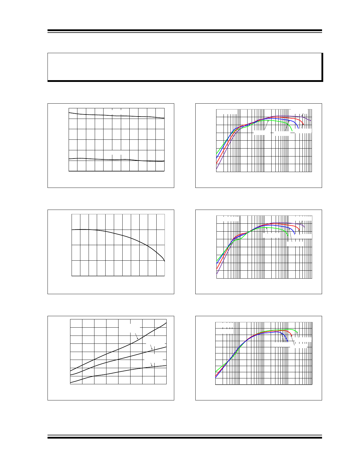
FIGURE 2-1:
Undervoltage Lockout
(UVLO) vs. Ambient Temperature.
FIGURE 2-2:
V
FB
Voltage vs. Ambient
Temperature and V
IN.
FIGURE 2-3:
Maximum Output Current
vs. V
IN
(V
OUT
in Regulation with Max. 5% Drop).
FIGURE 2-4:
9.0V V
OUT
Efficiency vs.
I
OUT
.
FIGURE 2-5:
12.0V V
OUT
Efficiency vs.
I
OUT
.
FIGURE 2-6:
24.0V V
OUT
Efficiency vs.
I
OUT
.
Note:
The graphs and tables provided following this note are a statistical summary based on a limited number of
samples and are provided for informational purposes only. The performance characteristics listed herein
are not tested or guaranteed. In some graphs or tables, the data presented may be outside the specified
operating range (e.g., outside specified power supply range) and therefore outside the warranted range.
1.7
1.8
1.9
2
2.1
2.2
2.3
-40 -25 -10
5
20
35
50
65
80
95 110 125
UVLO Thresholds (V)
Ambient Temperature (°C)
UVLO Start
UVLO Stop
1.210
1.215
1.220
1.225
1.230
-40 -25 -10
5
20 35 50 65 80 95 110 125
Feedback V
o
ltage
(V)
Ambient Temperature (°C)
0
100
200
300
400
500
600
700
800
2.3
2.7
3.1
3.5
3.9
4.3
4.7
5.1
5.5
I
OUT
(mA)
V
IN
(V)
V
OUT
= 12V
L = 4.7 µH
V
OUT
= 9.0V
L = 4.7 µH
V
OUT
= 24V
L = 10 µH
20
30
40
50
60
70
80
90
100
0.1
1
10
100
1000
Efficiency
(%
)
I
OUT
(mA)
V
OUT
= 9.0V
V
IN
= 3.0V
V
IN
= 2.3V
V
IN
= 4.0V
V
IN
= 5.5V
20
30
40
50
60
70
80
90
100
0.1
1
10
100
1000
Efficiency
(%
)
I
OUT
(mA)
V
OUT
= 12.0V
V
IN
= 4.0V
V
IN
= 5.5V
V
IN
= 3.0V
V
IN
= 2.3V
0
10
20
30
40
50
60
70
80
90
100
0.1
1
10
100
1000
Efficiency
(%
)
I
OUT
(mA)
V
OUT
= 24V
V
IN
= 5.5V
V
IN
= 3.0V V
IN
= 4.0V
L = 10 µH
MCP1663
DS20005406A-page 6
2015 Microchip Technology Inc.
Note:
Unless otherwise indicated, V
IN
= 3.3V, I
OUT
= 20 mA, V
OUT
= 12V, C
IN
= C
OUT
= 10 µF, X7R ceramic,
L = 4.7 µH, T
A
= 25°C.
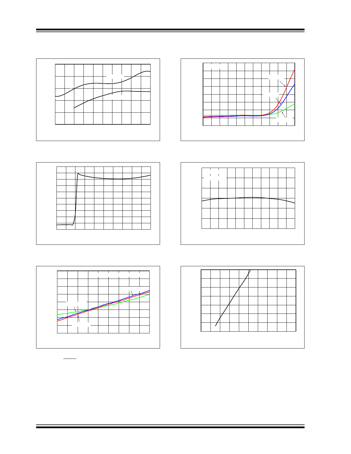
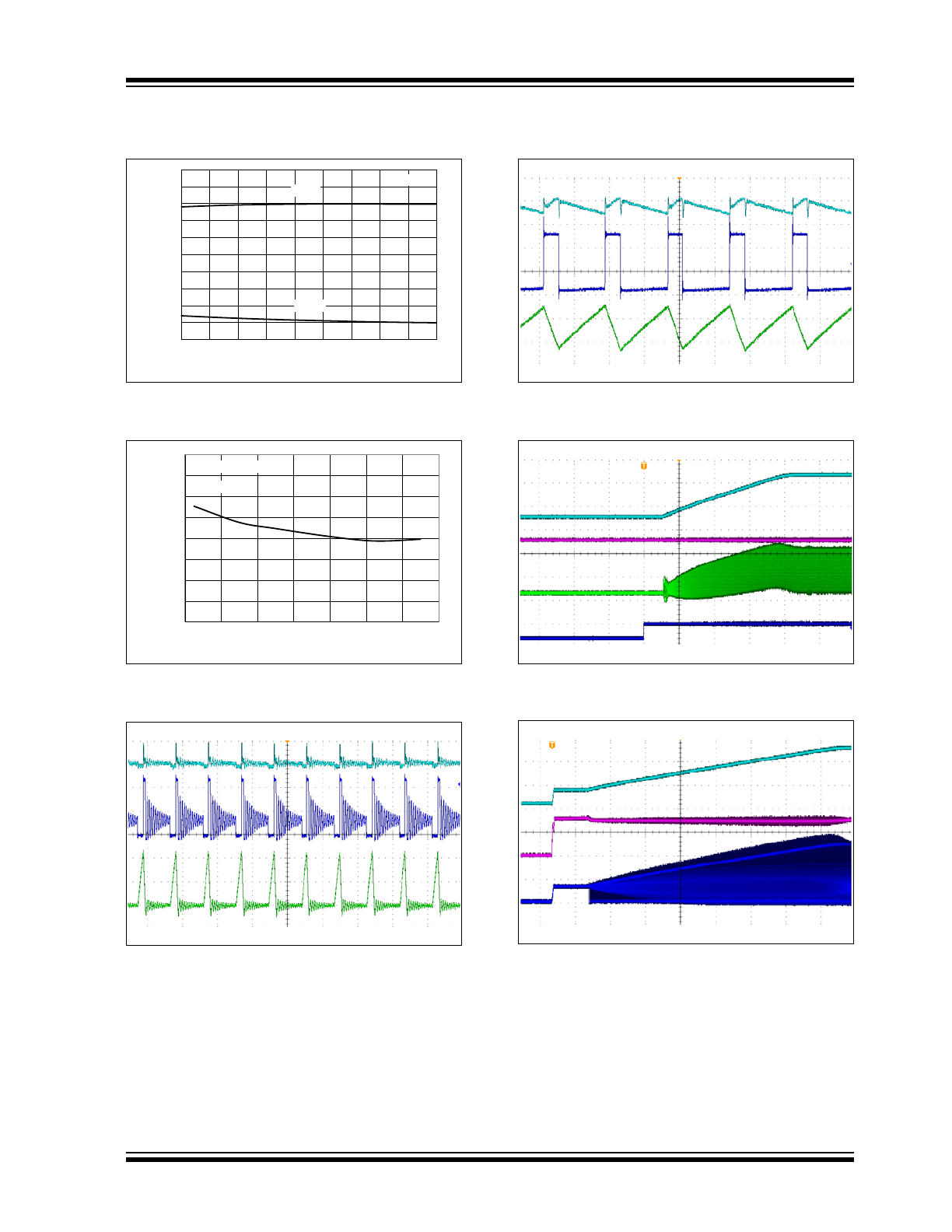
FIGURE 2-7:
Inductor Peak Current Limit
vs. Input Voltage.
FIGURE 2-8:
No Load Input Current, I
IN0
vs. V
IN
(EN = V
IN
).
FIGURE 2-9:
Shutdown Quiescent
Current,
I
QSHDN
vs. V
IN
(EN = GND).
FIGURE 2-10:
No Load Input Current,
I
IN0
vs. Ambient Temperature.
FIGURE 2-11:
f
SW
vs. Ambient
Temperature.
FIGURE 2-12:
PWM Pulse Skipping Mode
Threshold.
1
1.2
1.4
1.6
1.8
2
2.4 2.7
3
3.3
3.6
3.9
4.2
4.5
4.8
5.1 5.4
Inductor Peak Current (A)
Input Voltage (V)
V
OUT
= 24V
V
OUT
= 12V
0
30
60
90
120
150
180
210
240
270
300
1.4 1.8 2.2 2.6
3
3.4 3.8 4.2 4.6
5
5.4
I
Q
PWM Mode (µA)
Input Voltage (V)
0
0.1
0.2
0.3
0.4
0.5
0.6
0.7
0.8
1.8
2.2
2.6
3
3.4
3.8
4.2
4.6
5
5.4
I
Q
Shutdow
n Mode
(µA)
Input Voltage (V)
V
OUT
= 6.0V
V
OUT
= 12.0V
V
OUT
= 32.0V
Note: Without FB Resistor Divider Current
0
200
400
600
800
1000
1200
1400
1600
-40 -25 -10
5
20 35 50 65 80 95 110 125
I
Q
PWM Mode (µA)
Ambient Temperature (°C)
V
IN
= 3.0V
V
IN
= 5.5V
V
OUT
= 12V
V
IN
= 2.3V
425
450
475
500
525
550
575
-40 -25 -10
5
20
35
50
65
80
95 110 125
Sw
itching Frequency
(kHz)
Ambient Temperature (°C)
V
IN
= 3.5V
I
OUT
= 150 mA
2.0
2.5
3.0
3.5
4.0
4.5
5.0
5.5
0
1
2
3
4
5
6
7
8
9
10
V
IN
(V)
I
OUT
(mA)
2015 Microchip Technology Inc.
DS20005406A-page 7
MCP1663
Note:
Unless otherwise indicated, V
IN
= 3.3V, I
OUT
= 20 mA, V
OUT
= 12V, C
IN
= C
OUT
= 10 µF, X7R ceramic,
L = 4.7 µH, T
A
= 25°C.
FIGURE 2-13:
Enable Threshold vs. Input
Voltage.
FIGURE 2-14:
N-Channel Switch R
DSON
vs. V
IN
.
FIGURE 2-15:
12.0V V
OUT
Light Load
PWM Mode Waveforms.
FIGURE 2-16:
High-Load PWM Mode
Waveforms.
FIGURE 2-17:
12.0V Start-Up by Enable.
FIGURE 2-18:
12.0V Start-Up
(V
IN
= V
ENABLE
).
0
10
20
30
40
50
60
70
80
90
100
2.3
2.6
2.9
3.2
3.5
3.8
4.1
4.4
4.7
5
Enable Thresholds (%
of
V
IN
)
Input Voltage (V)
EN V
IL
EN V
IH
I
OUT
= 1 mA
0
0.1
0.2
0.3
0.4
0.5
0.6
0.7
0.8
2.4
2.8
3.2
3.6
4
4.4
4.8
5.2
Sw
itch R
DS(ON)
(Ohms)
Input Voltage (V)
I
OUT
= 100 mA
V
IN
= 5V
2 µs/div
V
OUT
20 mV/div, AC Coupled, 20 MHz BW
I
OUT
= 5 mA
V
SW
5 V/div
I
L
100 mA/div
1 µs/div
V
OUT
50 mV/div, AC Coupled
20 MHz BW
I
OUT
= 100 mA
V
SW
5 V/div
I
L
500 mA/div
V
OUT
5 V/div
I
OUT
= 15 mA
V
EN
5 V/div
I
L
500 mA/div
800 µs/div
V
IN
5 V/div
V
OUT
5 V/div
I
OUT
= 15 mA
V
SW
5 V/div
V
IN
2 V/div
400 µs/div
MCP1663
DS20005406A-page 8
2015 Microchip Technology Inc.
Note:
Unless otherwise indicated, V
IN
= 3.3V, I
OUT
= 20 mA, V
OUT
= 12V, C
IN
= C
OUT
= 10 µF, X7R ceramic,
L = 4.7 µH, T
A
= 25°C.
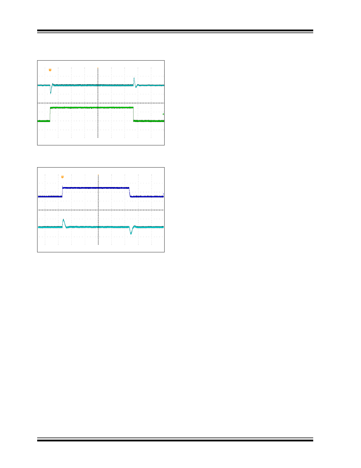
FIGURE 2-19:
12.0V V
OUT
Load Transient
Waveforms.
FIGURE 2-20:
12.0V V
OUT
Line Transient
Waveforms.
2 ms/div
V
OUT
200 mV/div, AC Coupled
I
OUT
20 mA/div
Step from 20 mA to 50 mA
800 us/div
V
OUT
100 mV/div, AC Coupled
V
IN
3 V/div
Step from 3.3V to 5.0V
I
OUT
= 60 mA
2015 Microchip Technology Inc.
DS20005406A-page 9
MCP1663
3.0
PIN DESCRIPTIONS
The descriptions of the pins are listed in
Table 3-1
.
3.1
Feedback Voltage Pin (V
FB
)
The V
FB
pin is used to provide output voltage regulation
by using a resistor divider. The V
FB
voltage is 1.227V
typical.
3.2
Signal Ground Pin (S
GND
)
The signal ground pin is used as a return for the
integrated reference voltage and error amplifier. The
signal ground and power ground must be connected
externally in one point.
3.3
Switch Node Pin (SW)
Connect the inductor from the input voltage to the SW
pin. The SW pin carries inductor current, which is 1.8A
peak typically. The integrated N-Channel switch drain
is internally connected to the SW node.
3.4
Not Connected (NC)
This is an unconnected pin.
3.5
Power Supply Input Voltage Pin
(V
IN
)
Connect the input voltage source to V
IN
. The input
source must be decoupled from GND with a 4.7 µF
minimum capacitor.
3.6
Power Ground Pin (P
GND
)
The power ground pin is used as a return for the
high-current N-Channel switch. The signal ground and
power ground must be connected externally in one
point.
3.7
Enable Pin (EN)
The EN pin is a logic-level input used to enable or
disable device switching and lower quiescent current
while disabled. A logic high (>85% of V
IN
) will enable
the regulator output. A logic low (<7.5% of V
IN
) will
ensure that the regulator is disabled.
3.8
Exposed Thermal Pad (EP)
There is no internal electrical connection between the
Exposed Thermal Pad (EP) and the S
GND
and P
GND
pins. They must be connected to the same potential on
the PCB.
3.9
Ground Pin (GND)
The ground or return pin is used for circuit ground
connection. The length of the trace from the input cap
return, the output cap return and the GND pin must be
as short as possible to minimize noise on the GND pin.
The 5-lead SOT-23 package uses a single ground pin.
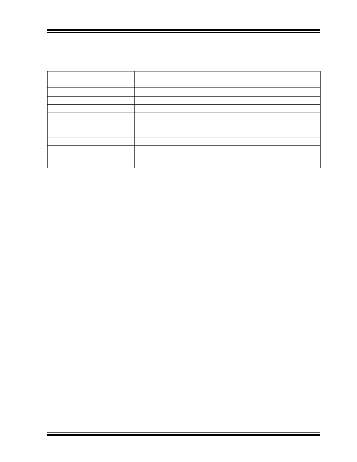
TABLE 3-1:
PIN FUNCTION TABLE
MCP1663
2x3 TDFN
MCP1663
SOT-23
Symbol
Description
1
3
V
FB
Feedback Voltage Pin
2
—
S
GND
Signal Ground Pin (TDFN only)
3
1
SW
Switch Node, Boost Inductor Input Pin
4, 6
—
NC
Not Connected
5
5
V
IN
Input Voltage Pin
7
—
P
GND
Power Ground Pin (TDFN only)
8
4
EN
Enable Control Input Pin
9
—
EP
Exposed Thermal Pad (EP); must be connected to Ground.
(TDFN only)
—
2
GND
Ground Pin (SOT-23 only)

MCP1663
DS20005406A-page 10
2015 Microchip Technology Inc.
NOTES: