
2014-2015 Microchip Technology Inc.
DS20005316E-page 1
MCP1662
Features
• 36V, 800 m
Integrated Switch
• Up to 92% Efficiency
• Drive LED Strings in Constant Current
• 1.3A Peak Input Current Limit:
- I
LED
up to 200 mA @ 5.0V V
IN
, 4 White LEDs
- I
LED
up to 125 mA @ 3.3V V
IN
, 4 White LEDs
- I
LED
up to 100 mA @ 4.2V V
IN
, 8 White LEDs
• Input Voltage Range: 2.4V to 5.5V
• Feedback Voltage Reference: V
FB
= 300 mV
• Undervoltage Lockout (UVLO):
- UVLO @ V
IN
Rising: 2.3V, typical
- UVLO @ V
IN
Falling: 1.85V, typical
• Sleep Mode with 20 nA Typical Quiescent Current
• PWM Operation: 500 kHz Switching Frequency
• Cycle-by-Cycle Current Limiting
• Internal Compensation
• Open Load Protection (OLP) in the Event of:
- Feedback pin shorted to GND (prevent
excessive current into LEDs)
- Disconnected LED string (prevent overvoltage
to the converter’s Output and SW pin)
• Overtemperature Protection
• Available Packages:
- 5-Lead SOT-23
- 8-Lead 2x3 TDFN
Applications
• Two and Three-Cell Alkaline or NiMH/NiCd White
LED Driver for Backlighting Products
• Li-Ion Battery LED Lighting Application
• Camera Flash
• LED Flashlights and Backlight Current Source
• Medical Equipment
• Portable Devices:
- Handheld Gaming Devices
- GPS Navigation Systems
- LCD Monitors
- Portable DVD Players
General Description
The MCP1662 device is a compact, space-efficient,
fixed-frequency, non-synchronous step-up converter
optimized to drive LED strings with constant current
from a two- or three-cell alkaline or lithium Energizer
®
,
or NiMH/NiCd, or one-cell Lithium-Ion or Li-Polymer
batteries.
The device integrates a 36V, 800 m
low-side switch,
which is protected by the 1.3A cycle-by-cycle inductor
peak current limit operation. All compensation and pro-
tection circuitry is integrated to minimize the number of
external components.
The internal feedback (V
FB
) voltage is set to 300 mV for
low power dissipation when sensing and regulating the
LED current. A single resistor sets the LED current.
The device features an Undervoltage Lockout (UVLO)
that avoids start-up with low inputs or discharged bat-
teries for two-cell-powered applications.
There is an open load protection (OLP) which turns off
the operation in situations when the LED string is acci-
dentally disconnected or the feedback pin is short-cir-
cuited to GND.
For standby applications (EN = GND), the device stops
switching, enters into Sleep mode and consumes
20 nA typical of input current.
Package Types
* Includes Exposed Thermal Pad (EP); see
Table 3-1
.
MCP1662
SOT-23
MCP1662
2x3 TDFN*
V
FB
GND
EN
1
2
3
5
4
V
IN
SW
SW
S
GND
NC
P
GND
NC
1
2
3
4
8
7
6
5
V
IN
EN
V
FB
EP
9
High-Voltage Step-Up LED Driver with UVLO and Open Load Protection
MCP1662
DS20005316E-page 2
2014-2015 Microchip Technology Inc.
Typical Application
V
IN
GND
V
FB
C
OUT
10 µF
C
IN
4.7 – 30 µF
L
4.7 – 10 µH
SW
EN
+
-
ALKAL
INE
ON
OFF
MCP1662
+
-
ALAKL
INE
V
IN
2.4V – 3.0V
LED6
12
R
SET
LED1
I
LED
= 25 mA
I
LED
=
0.3V
R
SET
LED2
V
FB
= 0.3V
Maximum LED Current in Regulation vs. Input Voltage, T
A
= + 25°C
V
OUT
0
50
100
150
200
250
2
2.5
3
3.5
4
4.5
5
5.5
I
OUT
(mA)
V
IN
(V)
4
wLEDs
, L = 4.7 µH
8 wLEDs, L = 10 µH
L
= 4.7 µH for maximum 4 white LEDs
L
= 10 µH for 5 to 10 white LEDs
C
IN
= 4.7-10 µF for V
IN
> 2.5V
C
IN
= 20-30 µF for V
IN
< 2.5V
D
MBR0540
I
LED
2014-2015 Microchip Technology Inc.
DS20005316E-page 3
MCP1662
1.0
ELECTRICAL
CHARACTERISTICS
Absolute Maximum Ratings †
V
SW
– GND .....................................................................+36V
EN, V
IN
– GND ...............................................................+6.0V
V
FB
...............................................................................+0.35V
Power Dissipation ....................................... Internally Limited
Storage Temperature .................................... -65
°
C to +150
°
C
Ambient Temperature with Power Applied .... -40
°
C to +125
°
C
Operating Junction Temperature................... -40
°
C to +150
°
C
ESD Protection on All Pins:
HBM ................................................................. 4 kV
MM ..................................................................300V
† Notice: Stresses above those listed under “Maximum
Ratings” may cause permanent damage to the device.
This is a stress rating only and functional operation of
the device at those or any other conditions above those
indicated in the operational sections of this specifica-
tion is not intended. Exposure to maximum rating con-
ditions for extended periods may affect device
reliability.
DC AND AC CHARACTERISTICS
Electrical Specifications: Unless otherwise specified, all limits apply for typical values at ambient temperature
T
A
= +25°C, V
IN
= 3.3V, V
OUT
= 9V or 3 white LEDs (V
F
= 2.75V @ I
F
= 20 mA or V
F
= 3.1V @ I
F
= 100 mA),
I
LED
= 20 mA, C
IN
= C
OUT
= 10 µF, X7R ceramic, L = 4.7 µH.
Boldface specifications apply over the controlled T
A
range of -40°C to +125°C.
Parameters
Sym.
Min.
Typ.
Max.
Units
Conditions
Input Voltage Range
V
IN
2.4
—
5.5
V
Note 1
Undervoltage Lockout (UVLO)
UVLO
START
—
2.3
—
V
V
IN
rising, I
LED
= 20 mA
UVLO
STOP
—
1.85
—
V
V
IN
falling, I
LED
= 20 mA
Maximum Output Voltage
V
OUTmax
—
—
32
V
Maximum Output Current
I
OUT
—
100
—
mA
4.2V V
IN
, 8 LEDs
125
—
mA
3.3V V
IN
, 4 LEDs
200
—
mA
5.0V V
IN
, 4 LEDs
Feedback Voltage Reference
V
FB
275
300
325
mV
Feedback Open Load
Protection (OLP) Threshold
V
FB_OLP
—
50
—
mV
V
FB
falling (
Note 2
)
Feedback Input Bias Current
I
VFB
—
0.005
—
µA
Shutdown Quiescent Current
I
QSHDN
—
0.02
—
µA
EN = GND
NMOS Peak Switch Current
Limit
I
N(MAX)
—
1.3
—
A
Note 2
NMOS Switch Leakage
I
NLK
—
0.4
—
µA
V
IN
= V
SW
= 5V;
V
OUT
= 5.5V
V
EN
= V
FB
= GND
NMOS Switch ON Resistance
R
DS(ON)
—
0.8
—
V
IN
= 5V,
I
LED
= 100 mA,
4 series white LEDs
(
Note 2
)
Feedback Voltage
Line Regulation
|(
V
FB
/V
FB
)/
V
IN
|
—
0.25
—
%/V
V
IN
= 3.0V to 5V
Maximum Duty Cycle
DC
MAX
—
90
—
%
Note 2
Switching Frequency
f
SW
425
500
575
kHz
±15%
EN Input Logic High
V
IH
85
—
—
% of V
IN
Note 1:
Minimum input voltage in the range of V
IN
(V
IN
< 5.5V < V
OUT
) depends on the maximum duty cycle
(DC
MAX
) and on the output voltage (V
OUT
), according to the boost converter equation:
V
INmin
= V
OUT
x (1 – DC
MAX
). Output voltage is equal to the LED voltage plus the voltage on the sense
resistor (V
OUT
= V
LED
+ V_R
SET
).
2:
Determined by characterization, not production tested.
MCP1662
DS20005316E-page 4
2014-2015 Microchip Technology Inc.
EN Input Logic Low
V
IL
—
—
7.5
% of V
IN
EN Input Leakage Current
I
ENLK
—
0.025
—
µA
V
EN
= 5V
Start-up Time
t
SS
—
100
—
µs
EN Low-to-High,
90% of I
LED
(
Note 2
,
Figure 2-10
)
Thermal Shutdown
Die Temperature
T
SD
—
150
—
°C
Die Temperature Hysteresis
T
SDHYS
—
15
—
°C
TEMPERATURE SPECIFICATIONS
Electrical Specifications: Unless otherwise specified, all limits apply for typical values at ambient temperature
T
A
= +25°C, V
IN
= 3.0V, I
OUT
= 20 mA, V
OUT
= 12V, C
IN
= C
OUT
= 10 µF, X7R ceramic, L = 4.7 µH.
Boldface specifications apply over the air-forced T
A
range of -40°C to +125°C.
Parameters
Sym.
Min.
Typ.
Max.
Units
Conditions
Temperature Ranges
Operating Junction Temperature
Range
T
J
-40
—
+125
°C
Steady State
Storage Temperature Range
T
A
-65
—
+150
°C
Maximum Junction Temperature
T
J
—
—
+150
°C
Transient
Package Thermal Resistances
Thermal Resistance, 5L-SOT-23
JA
—
201.0
—
°C/W
Thermal Resistance, 8L 2x3 TDFN
JA
—
52.5
—
°C/W
DC AND AC CHARACTERISTICS (CONTINUED)
Electrical Specifications: Unless otherwise specified, all limits apply for typical values at ambient temperature
T
A
= +25°C, V
IN
= 3.3V, V
OUT
= 9V or 3 white LEDs (V
F
= 2.75V @ I
F
= 20 mA or V
F
= 3.1V @ I
F
= 100 mA),
I
LED
= 20 mA, C
IN
= C
OUT
= 10 µF, X7R ceramic, L = 4.7 µH.
Boldface specifications apply over the controlled T
A
range of -40°C to +125°C.
Parameters
Sym.
Min.
Typ.
Max.
Units
Conditions
Note 1:
Minimum input voltage in the range of V
IN
(V
IN
< 5.5V < V
OUT
) depends on the maximum duty cycle
(DC
MAX
) and on the output voltage (V
OUT
), according to the boost converter equation:
V
INmin
= V
OUT
x (1 – DC
MAX
). Output voltage is equal to the LED voltage plus the voltage on the sense
resistor (V
OUT
= V
LED
+ V_R
SET
).
2:
Determined by characterization, not production tested.
2014-2015 Microchip Technology Inc.
DS20005316E-page 5
MCP1662
2.0
TYPICAL PERFORMANCE CURVES
Note: Unless otherwise indicated: V
IN
= 3.3V, I
LED
= 20 mA, V
OUT
= 12V or 4 white LEDs (V
F
= 2.75V @ I
F
= 20 mA or
V
F
= 3.1V @ I
F
= 100 mA), C
IN
= C
OUT
= 10 µF, X7R ceramic, L = 4.7 µH.
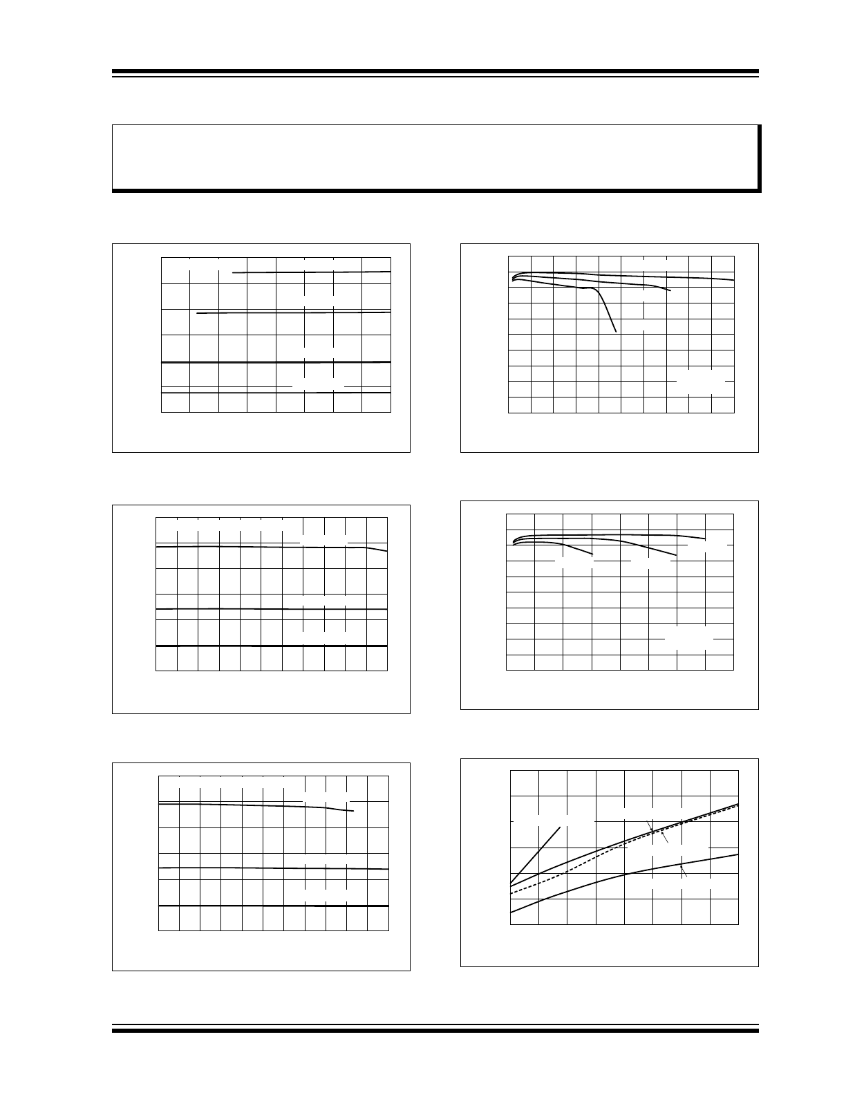
FIGURE 2-1:
4 White LEDs, I
LED
vs. V
IN
.
FIGURE 2-2:
4 White LEDs, I
LED
vs.
Ambient Temperature.
FIGURE 2-3:
8 White LEDs, I
LED
vs.
Ambient Temperature.
FIGURE 2-4:
4 White LEDs, Efficiency vs.
I
LED
.
FIGURE 2-5:
8 White LEDs, Efficiency vs.
I
LED
.
FIGURE 2-6:
Maximum I
LED
vs. V
IN
.
Note:
The graphs and tables provided following this note are a statistical summary based on a limited number of
samples and are provided for informational purposes only. The performance characteristics listed herein
are not tested or guaranteed. In some graphs or tables, the data presented may be outside the specified
operating range (e.g., outside specified power supply range) and therefore outside the warranted range.
0
25
50
75
100
125
150
2.3
2.7
3.1
3.5
3.9
4.3
4.7
5.1
5.5
LED Current (mA)
Input Voltage (V)
R
SET
= 15
ȍ
R
SET
= 6.2
ȍ
R
SET
= 2.2
ȍ
R
SET
= 3.2
ȍ
4 x wLED, L = 4.7 µH
0
20
40
60
80
100
120
-40 -25 -10
5
20
35
50
65
80
95 110 125
LED Current (mA)
Ambient Temperature (
o
C)
R
SET
= 15
ȍ
4 x wLED, L = 4.7 µH, V
IN
= 3.3V
R
SET
= 6.2
ȍ
R
SET
= 3.2
ȍ
0
20
40
60
80
100
120
-40 -25 -10
5
20
35
50
65
80
95 110 125
LED Current (mA)
Ambient Temperature (
o
C)
R
SET
= 15
ȍ
8 x wLED, L = 10 µH, V
IN
= 4.2V
R
SET
= 6.2
ȍ
R
SET
= 3.2
ȍ
0
10
20
30
40
50
60
70
80
90
100
0
25
50
75 100 125 150 175 200 225 250
Efficiency
(%
)
I
LED
(mA)
V
IN
= 3.0V
V
IN
= 4.0V
V
IN
= 5.5V
L = 4.7 µH,
4 wLEDs
0
10
20
30
40
50
60
70
80
90
100
0
20
40
60
80
100
120
140
160
Efficiency
(%
)
I
LED
(mA)
V
IN
= 4.0V
V
IN
= 5.5V
V
IN
= 3.0V
L = 10 µH,
8 wLEDs
0
50
100
150
200
250
300
2.3
2.7
3.1
3.5
3.9
4.3
4.7
5.1
5.5
LED Current (mA)
Input Voltage (V)
8 wLEDs, L = 10 µH
4 wLEDs, L = 4.7 µH
5 wLEDs, L = 10 µH
2 wLEDs, L = 4.7 µH
MCP1662
DS20005316E-page 6
2014-2015 Microchip Technology Inc.
Note: Unless otherwise indicated: V
IN
= 3.3V, I
LED
= 20 mA, V
OUT
= 12V or 4 white LEDs (V
F
= 2.75V @ I
F
= 20 mA or
V
F
= 3.1V @ I
F
= 100 mA), C
IN
= C
OUT
= 10 µF, X7R ceramic, L = 4.7 µH.
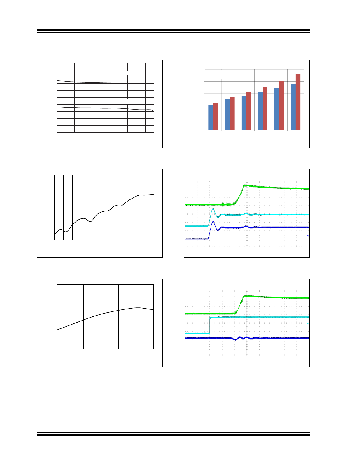
FIGURE 2-7:
Undervoltage Lockout
(UVLO) vs. Ambient Temperature.
FIGURE 2-8:
Shutdown Quiescent
Current,
I
QSHDN
, vs. V
IN
(EN = GND).
FIGURE 2-9:
Switching Frequency, f
SW
vs. Ambient Temperature.
FIGURE 2-10:
Soft Start Time vs. Number
of LEDs.
FIGURE 2-11:
Start-Up When
V
IN
= V
ENABLE
.
FIGURE 2-12:
Start-Up After Enable.
1.5
1.6
1.7
1.8
1.9
2
2.1
2.2
2.3
2.4
2.5
-40 -25 -10
5
20
35
50
65
80
95 110 125
UVLO Thresholds (V)
Ambient Temperature (
o
C)
UVLO Stop
UVLO Start
0
10
20
30
40
50
2.2 2.5 2.8 3.1 3.4 3.7 4.0 4.3 4.6 4.9 5.2 5.5
Shutdow
n Iq
(nA)
Input Voltage (V)
450
475
500
525
550
-40 -25 -10
5
20
35
50
65
80
95 110 125
Sw
itching Frequency
(kHz)
Ambient Temperature (°C)
0
50
100
150
200
250
3
4
5
6
7
8
Start-up T
ime
(µs)
Number of LEDs
Blue Bars - I
LED
= 20 mA
Red Bars - I
LED
= 40 mA
I
LED
10 mA/div
V
EN
2V/div
V
IN
2V/div
3 LEDs, I
LED
= 20 mA
40 µs/div
I
LED
10 mA/div
V
EN
2V/div
V
IN
2V/div
3 LED, I
LED
= 20 mA
40 µs/div
2014-2015 Microchip Technology Inc.
DS20005316E-page 7
MCP1662
Note: Unless otherwise indicated: V
IN
= 3.3V, I
LED
= 20 mA, V
OUT
= 12V or 4 white LEDs (V
F
= 2.75V @ I
F
= 20 mA or
V
F
= 3.1V @ I
F
= 100 mA), C
IN
= C
OUT
= 10 µF, X7R ceramic, L = 4.7 µH.
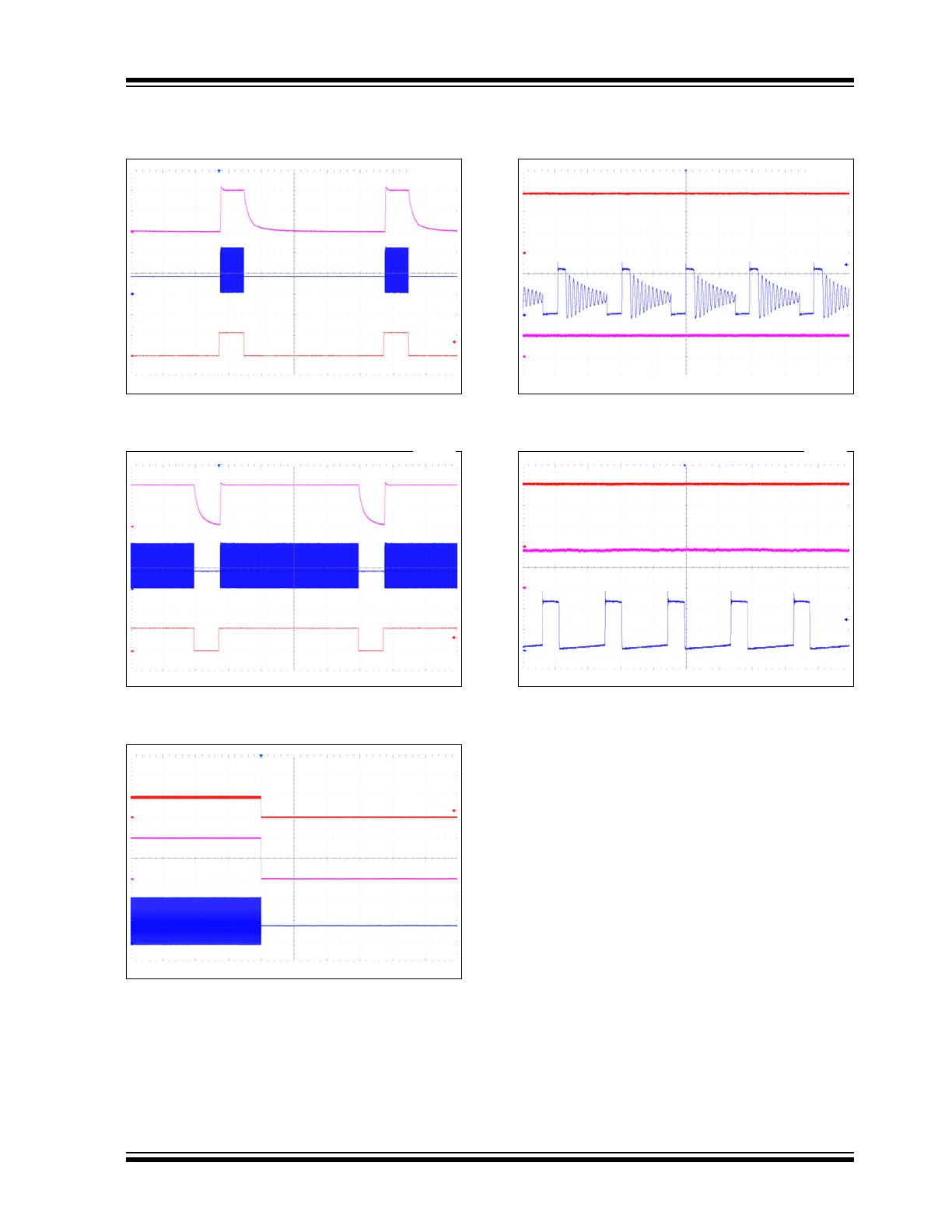
FIGURE 2-13:
100 Hz PWM Dimming, 15%
Duty Cycle.
FIGURE 2-14:
100 Hz PWM Dimming, 85%
Duty Cycle.
FIGURE 2-15:
Open Load (LED Fail or FB
to GND) Response.
FIGURE 2-16:
3.3V Input, 20 mA 3 White
LEDs PWM Discontinuous Mode Waveforms.
FIGURE 2-17:
3.3V Input, 100 mA 3 White
LEDs PWM Continuous Mode Waveforms.
I
LED
10 mA/div
V
SW
4V/div
V
EN
3V/div
2 ms/div
3 LEDs
I
LED
100 mA/div
V
SW
4V/div
V
EN
3V/div
2 ms/div
V
FB
300 mV/div
I
LED
10 mA/div
V
SW
4V/div
50 ms/div
V
OUT
3V/div
I
LED
20 mA/div
V
SW
4V/div
1 µs/div
3 LEDs
V
OUT
3V/div
I
LED
50 mA/div
V
SW
4V/div
1 µs/div
3 LEDs
3 LEDs
3 LEDs
MCP1662
DS20005316E-page 8
2014-2015 Microchip Technology Inc.
3.0
PIN DESCRIPTIONS
The descriptions of the pins are listed in
Table 3-1
.
3.1
Feedback Voltage Pin (V
FB
)
The V
FB
pin is used to regulate the voltage across the
R
SET
sense resistor to 300 mV to keep the output LED
current in regulation. Connect the cathode of the LED
to the V
FB
pin.
3.2
Signal Ground Pin (S
GND
)
The signal ground pin is used as a return for the inte-
grated reference voltage and error amplifier. The signal
ground and power ground must be connected exter-
nally in one point.
3.3
Switch Node Pin (SW)
Connect the inductor from the input voltage to the SW
pin. The SW pin carries inductor current and has a typ-
ical value of 1.3A peak. The integrated N-Channel
switch drain is internally connected to the SW node.
3.4
Not Connected (NC)
This is an unconnected pin.
3.5
Power Supply Input Voltage Pin
(V
IN
)
Connect the input voltage source to V
IN
. The input
source should be decoupled from GND with a 4.7 µF
minimum capacitor.
3.6
Power Ground Pin (P
GND
)
The power ground pin is used as a return for the
high-current N-Channel switch. The P
GND
and S
GND
pins are connected externally. The signal ground and
power ground must be connected externally in one
point.
3.7
Enable Pin (EN)
The EN pin is a logic-level input used to enable or dis-
able device switching and lower quiescent current
while disabled. A logic high (>85% of V
IN
) will enable
the regulator output. A logic low (<7.5% of V
IN
) will
ensure that the regulator is disabled.
3.8
Exposed Thermal Pad (EP)
There is no internal electrical connection between the
Exposed Thermal Pad (EP) and the S
GND
and P
GND
pins. They must be connected to the same potential on
the Printed Circuit Board (PCB).
3.9
Ground Pin (GND)
The ground or return pin is used for circuit ground con-
nection. The length of the trace from the input cap
return, the output cap return and the GND pin must be
as short as possible to minimize noise on the GND pin.
The 5-lead SOT-23 package uses a single ground pin.
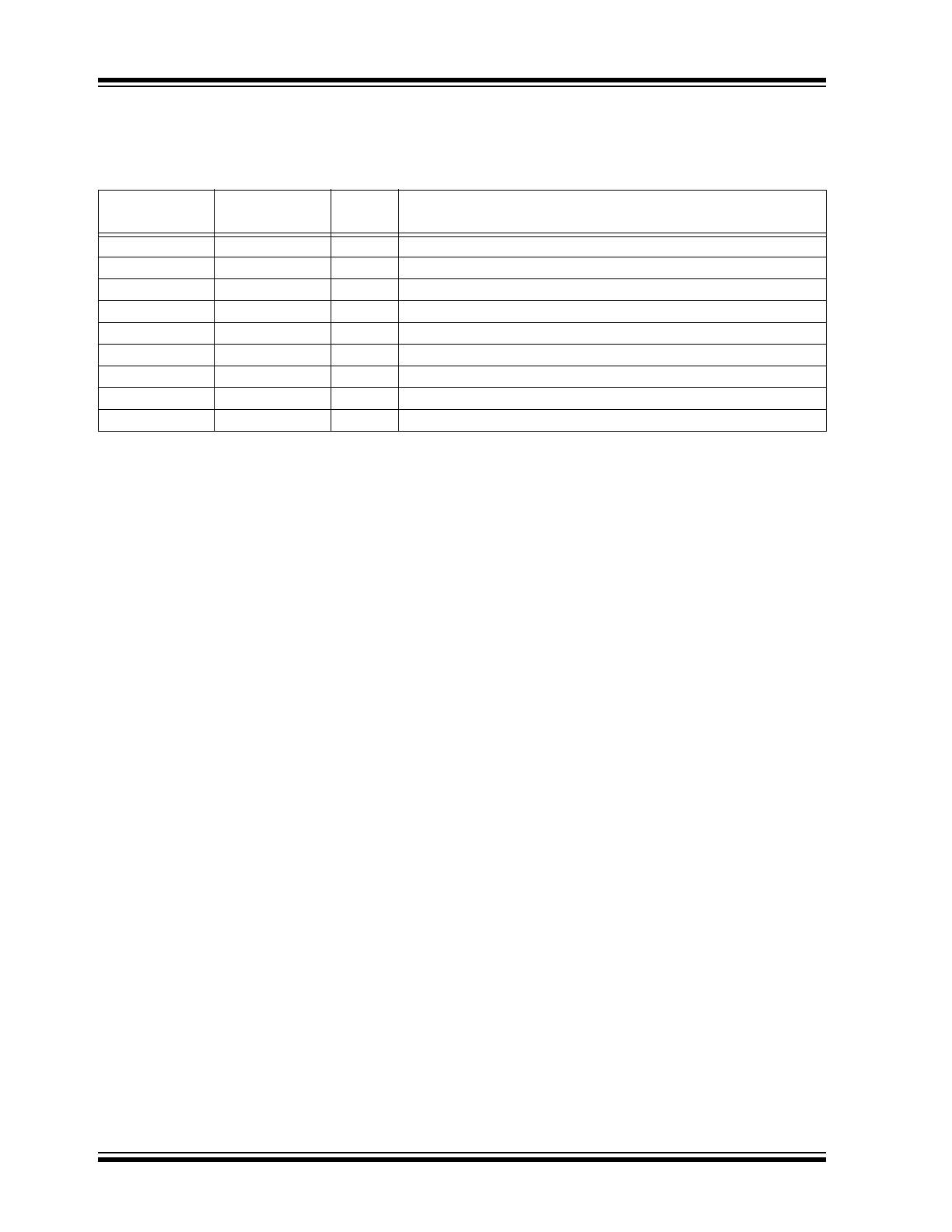
TABLE 3-1:
PIN FUNCTION TABLE
MCP1662
SOT-23
MCP1662
2x3 TDFN
Symbol
Description
3
1
V
FB
Feedback Voltage Pin
—
2
S
GND
Signal Ground Pin
1
3
SW
Switch Node, Boost Inductor Input Pin
—
4, 6
NC
Not Connected
5
5
V
IN
Input Voltage Pin
—
7
P
GND
Power Ground Pin
4
8
EN
Enable Control Input Pin
—
9
EP
Exposed Thermal Pad (EP); must be connected to Ground
2
—
GND
Ground Pin

2014-2015 Microchip Technology Inc.
DS20005316E-page 9
MCP1662
4.0
DETAILED DESCRIPTION
4.1
Device Overview
The MCP1662 device is a fixed-frequency, synchro-
nous step-up converter, with a low-voltage reference of
300 mV, optimized to keep the output current constant
by regulating the voltage across the feedback resistor
(R
SET
). The MCP1662 integrates a peak current mode
architecture. It delivers high-efficiency conversion for
an LED lighting application when it is powered by two-
or three-cell alkaline, lithium, NiMH, NiCd, or single-cell
Lithium-Ion batteries. The maximum input voltage is
5.5V. A high level of integration lowers total system
cost, eases implementation and reduces board area.
The conventional boost converter with a high-voltage
reference has a high-voltage drop across the LED
series current limit resistor. The power dissipated in this
resistor, which is usually in series with the LED string,
reduces the total efficiency conversion of an LED driver
solution. Therefore, the voltage drop on the sense
resistor (R
SET
) that is used to regulate the LED current
must be low. In the case of MCP1662, the V
FB
value is
300 mV.
The device features controlled start-up voltage
(UVLO
START
= 2.3V) and open load protection, in case
the LED fails or a short circuit of the V
FB
pin to GND
occurs. If the V
FB
voltage drops to 50 mV typical, the
device stops switching and the output voltage will be
equal to the input voltage (minus a diode drop voltage).
This feature prevents damage to the device and LEDs
when there is an accidental drop in voltage.
The 800 m
, 36V integrated switch is protected by the
1.3A cycle-by-cycle inductor peak current limit opera-
tion. When the Enable pin is pulled to ground
(EN = GND), the device stops switching, enters into
Shutdown mode and consumes less than 50 nA of
input current (
Figure 2-8
).
4.2
Functional Description
The MCP1662 is a compact, high-efficiency, fixed
500 kHz frequency, step-up DC-DC converter. It oper-
ates as a constant current generator for applications
powered by two- or three-cell alkaline or lithium Ener-
gizer
®
batteries, or three-cell NiCd or NiMH batteries,
or one-cell Lithium-Ion or Li-Polymer batteries.
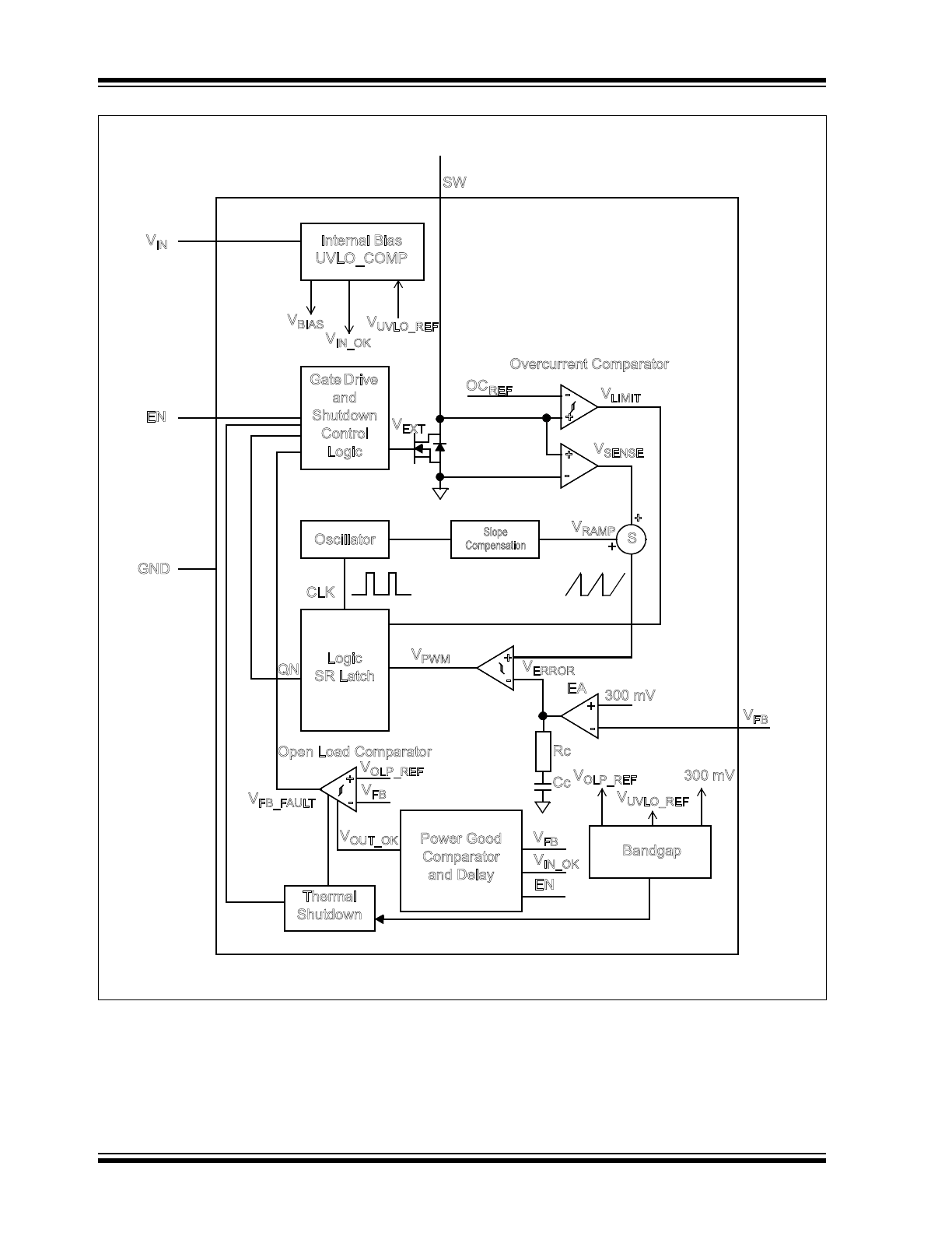
Figure 4-1
depicts the functional block diagram of the
MCP1662. It incorporates a Current mode control
scheme, in which the PWM ramp signal is derived from
the NMOS power switch current (V
SENSE
). This ramp
signal adds a slope ramp compensation signal (V
RAMP
)
and is compared to the output of the error amplifier
(V
ERROR
) to control the “on” time of the power switch.
MCP1662
DS20005316E-page 10
2014-2015 Microchip Technology Inc.
FIGURE 4-1:
MCP1662 Simplified Block Diagram.
EN
+
-
+
-
+
-
S
+
-
300 mV
V
FB
EA
GND
+
-
V
OLP_REF
V
FB
V
FB_FAULT
Cc
Rc
V
RAMP
V
ERROR
CLK
QN
V
EXT
V
FB
V
IN_OK
EN
V
BIAS
V
UVLO_REF
V
IN_OK
300 mV
V
UVLO_REF
V
SENSE
V
LIMIT
V
OUT_OK
V
IN
Internal Bias
UVLO_COMP
SW
Overcurrent Comparator
Slope
Compensation
Oscillator
Gate Drive
and
Shutdown
Control
Logic
Logic
SR Latch
Open Load Comparator
Thermal
Shutdown
Power Good
Comparator
and Delay
V
PWM
Bandgap
V
OLP_REF
+
+
REF
OC