2014 Microchip Technology Inc.
DS20005253A-page 1
MCP1642B/D
Features
• Up to 96% Typical Efficiency
• 1.8A Typical Peak Input Current Limit:
- I
OUT
> 175 mA @ 1.2V V
IN
, 3.3V V
OUT
- I
OUT
> 600 mA @ 2.4V V
IN
, 3.3V V
OUT
- I
OUT
> 800 mA @ 3.3V V
IN
, 5.0V V
OUT
- I
OUT
> 1A @ V
IN
> 3.6V, 5.0V V
OUT
• Low Start-Up Voltage: 0.65V, typical 3.3V V
OUT
@ 1 mA
• Low Operating Input Voltage: 0.35V, typical 3.3V
V
OUT
@ 1 mA
• Output Voltage Range:
- Reference Voltage, V
FB
= 1.21V
- 1.8V to 5.5V for the adjustable device option
- 1.8V, 3.0V, 3.3V and 5.0V for fixed V
OUT
options
• Maximum Input Voltage
V
OUT
< 5.5V
• PWM Operation: 1 MHz
- Low Noise, Anti-Ringing Control
• Power Good Open-Drain Output
• Internal Synchronous Rectifier
• Internal Compensation
• Inrush Current Limiting and Internal Soft-Start
• Selectable, Logic-Controlled Shutdown States:
- True Load Disconnect Option (MCP1642B)
- Input-to-Output Bypass Option (MCP1642D)
• Shutdown Current (All States): 1 µA
• Overtemperature Protection
• Available Packages:
- 8-Lead MSOP
- 8-Lead 2x3 DFN
Applications
• One, Two and Three-Cell Alkaline, Lithium
Ultimate and NiMH/NiCd Portable Products
• Single-Cell Li-Ion to 5V Converters
• PIC
®
MCU Power
• USB Emergency Backup Charger from Batteries
• Personal Medical Products
• Wireless Sensors
• Hand-Held Instruments
• GPS Receivers
• +3.3V to +5.0V Distributed Power Supply
General Description
The MCP1642B/D devices are compact,
high-efficiency, fixed-frequency, synchronous step-up
DC-DC converters. This family of devices provides an
easy-to-use power supply solution for applications
powered by either one-cell, two-cell, or three-cell
alkaline, Ultimate Lithium, NiCd, NiMH, one-cell Li-Ion
or Li-Polymer batteries.
Low-voltage technology allows the regulator to start-up
without high inrush current or output voltage overshoot
from a low voltage input. High efficiency is
accomplished by integrating the low-resistance
N-Channel Boost switch and synchronous P-Channel
switch. All compensation and protection circuitry are
integrated to minimize the number of external
components. An open-drain Power Good output is
provided to indicate when the output voltage is within
10% of regulation and facilitates the interface with an
MCU. For standby applications, MCP1642B provides a
“true output disconnect” from input to output while in
shutdown (EN = GND). An additional device option
(MCP1642D) is available and connects “input to output
bypass” while in shutdown. Both options consume less
than 1 µA of input current.
For the adjustable (ADJ) device options, the output
voltage is set by a small external resistor divider. Fixed
V
OUT
device options do not require external divider
resistors. Two package options, 8-lead MSOP and 8-
lead 2x3 DFN, are available.
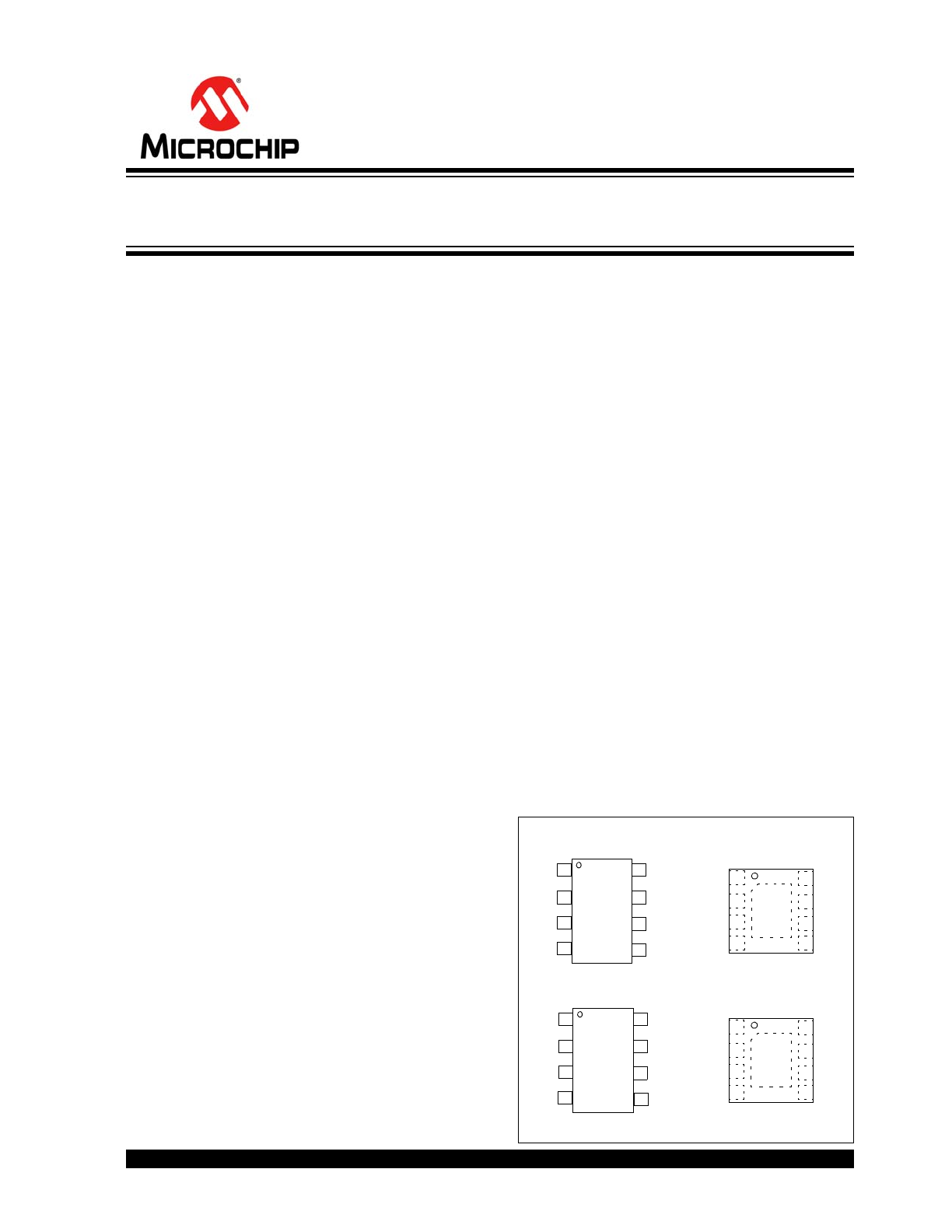
Package Types
PG
NC
V
OUT
S
GND
P
GND
1
2
3
4
8
7
6
5 SW
V
IN
EN
EP
9
P
GND
S
GND
PG
V
FB
V
OUT
S
GND
P
GND
1
2
3
4
8
7
6
5 SW
V
IN
EN
EP
9
6
1
2
3
8 V
IN
P
GND
EN
V
FB
PG
7 S
GND
5
4
SW
V
OUT
6
1
2
3
8 V
IN
EN
NC
PG
7
5
4
SW
V
OUT
MCP1642B/D-xx
MSOP
MCP1642B/D-xx
2x3 DFN*
MCP1642B/D-ADJ
MSOP
MCP1642B/D-ADJ
2x3 DFN*
* Includes Exposed Thermal Pad (EP); see
Table 3-1
.
1.8A Input Current Switch, 1 MHz Low-Voltage Start-Up
Synchronous Boost Regulator
MCP1642B/D
DS20005253A-page 2
2014 Microchip Technology Inc.
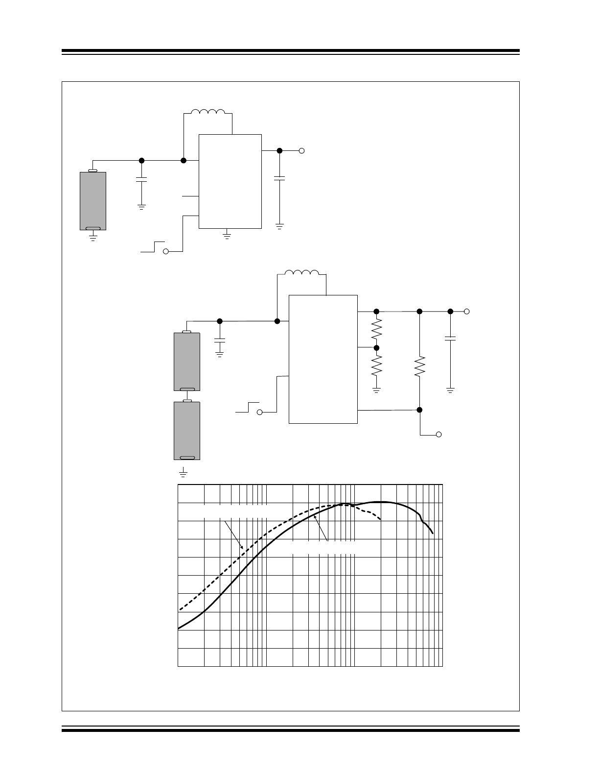
Typical Application
V
IN
GND
V
FB
V
OUT
5.0V
C
OUT
4.7...10 µF
C
IN
4.7...10 µF
L
4.7 µH
SW
976 k
309 k
EN
V
OUT
+
-
AL
KALINE
1 M
PG
ON
OFF
To PIC
MCU I/O
+
-
ALKAL
INE
R
TOP
R
BOT
R
PG
V
IN
GND
V
OUT
3.3V
C
OUT
4.7...10 µF
C
IN
4.7...10 µF
L
1
4.7 µH
SW
EN
V
OUT
+
- ALKAL
INE
PG
ON
OFF
NC
0
10
20
30
40
50
60
70
80
90
100
1
10
100
1000
Efficiency
(%
)
I
OUT
(mA)
V
IN
= 2.5V, V
OUT
= 5.0V
V
IN
= 1.2V, V
OUT
= 3.3V
MCP1642B-33
MCP1642D-ADJ
From PIC
®
MCU I/O
V
IN
= 0.9 to 1.6V
V
IN
= 1.8 to 3.2V
2014 Microchip Technology Inc.
DS20005253A-page 3
MCP1642B/D
1.0
ELECTRICAL
CHARACTERISTICS
Absolute Maximum Ratings †
EN, FB, V
IN,
V
SW
, V
OUT
– GND .......................... +6.5V
EN, FB ...... <maximum of V
OUT
or V
IN
> (GND – 0.3V)
Output Short-Circuit Current ...................... Continuous
Output Current Bypass Mode........................... 800 mA
Power Dissipation ............................ Internally Limited
Storage Temperature ..........................-65
°
C to +150
°
C
Ambient Temp. with Power Applied.......-40
°
C to +85
°
C
Operating Junction Temperature.........-40
°
C to +125
°
C
ESD Protection On All Pins:
HBM........................................................ 4 kV
MM......................................................... 300V
† Notice: Stresses above those listed under “Maximum
Ratings” may cause permanent damage to the device.
This is a stress rating only and functional operation of
the device at those or any other conditions above those
indicated in the operational sections of this
specification is not intended. Exposure to maximum
rating conditions for extended periods may affect
device reliability.
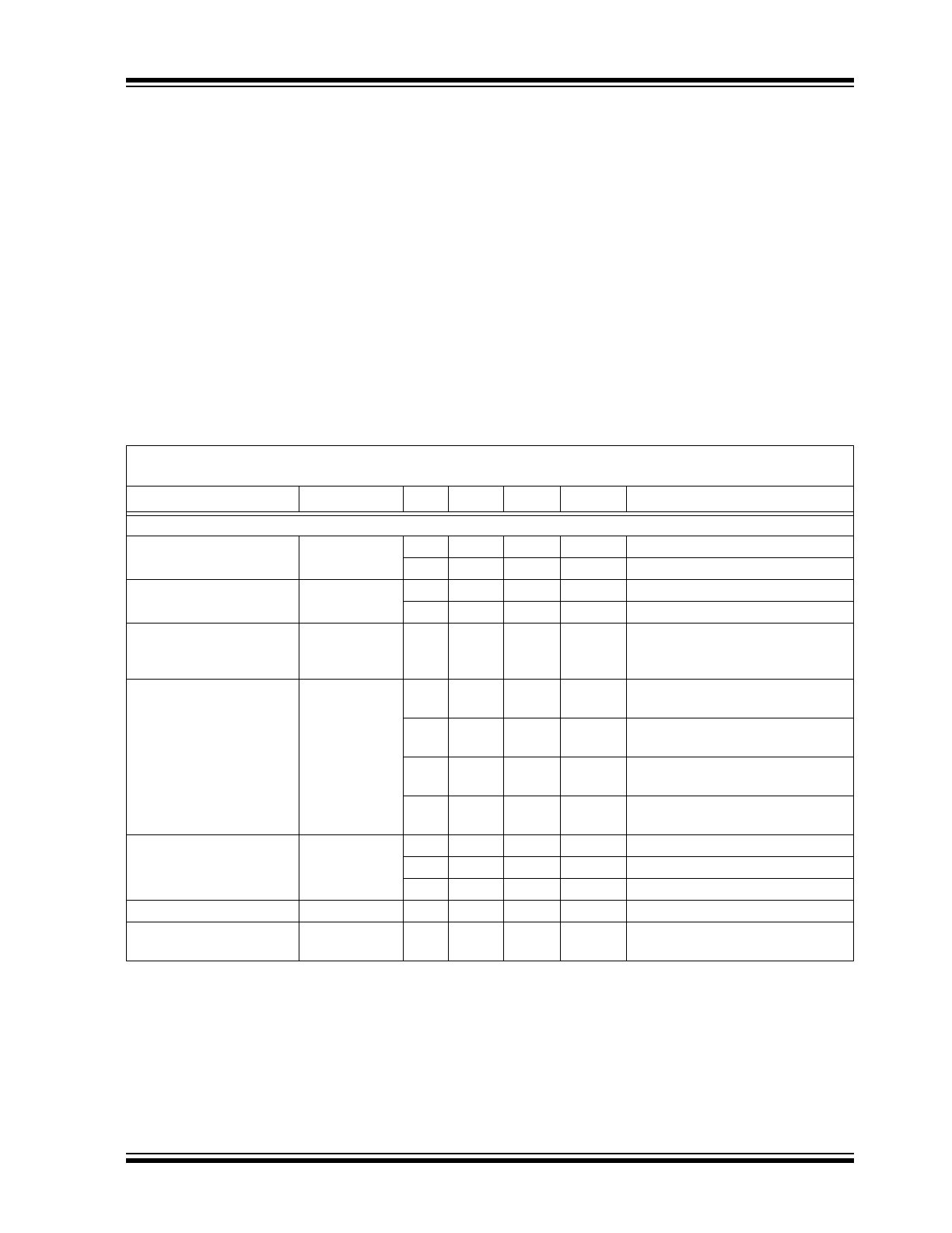
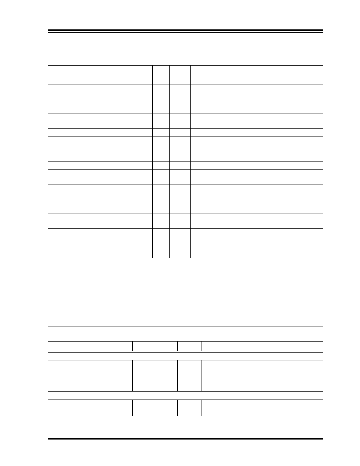
DC CHARACTERISTICS
Electrical Characteristics: Unless otherwise indicated, V
IN
= 1.2V, C
OUT
= C
IN
= 10 µF, L = 4.7 µH, V
OUT
= 3.3V,
I
OUT
= 15 mA, T
A
= +25°C, MCP1642B/D-ADJ. Boldface specifications apply over the T
A
range of -40
°
C to +85
°
C.
Parameters
Sym.
Min.
Typ.
Max.
Units
Conditions
Input Characteristics
Minimum Start-Up Voltage
V
IN
—
0.65
0.8
V
Note 1
—
0.9
1.8
V
MCP1642B/D-50,
Note 1
Minimum Input Voltage
After Start-Up
V
IN
—
0.35
—
V
Note 1
,
Note 5
—
0.5
—
V
Note 1
,
Note 5
, MCP1642B/D-50
Output Voltage Adjust.
Range
(MCP1642B/D-ADJ)
V
OUT
1.8
—
5.5
V
V
OUT
V
IN
(MCP1642B/D-ADJ);
Note 2
Output Voltage
(MCP1642B/D-XX)
V
OUT
—
1.8
—
V
V
IN
< 1.8V, MCP1642B/D-18,
Note 2
—
3.0
—
V
V
IN
< 3.0V, MCP1642B/D-30,
Note 2
—
3.3
—
V
V
IN
< 3.3V, MCP1642B/D-33,
Note 2
—
5.0
—
V
V
IN
< 5.0V, MCP1642B/D-50,
Note 2
Maximum Output Current
I
OUT
—
175
—
mA
1.2V V
IN
, 1.8V V
OUT
,
Note 5
—
300
—
mA
1.5V V
IN
, 3.3V V
OUT
,
Note 5
—
800
—
mA
3.3V V
IN
, 5.0V V
OUT
,
Note 5
Feedback Voltage
V
FB
1.173
1.21
1.247
V
Feedback Input
Bias Current
I
VFB
—
1.0
—
nA
Note 5
Note 1:
Resistive load, 1 mA.
2:
For V
IN
> V
OUT
, V
OUT
will not remain in regulation.
3:
I
QPWM
is measured from V
OUT
; V
OUT
is externally supplied with a voltage higher than the nominal 3.3V
output (device is not switching), no load. V
IN
quiescent current will vary with boost ratio. V
IN
quiescent
current can be estimated by: (I
QPWM
* (V
OUT
/V
IN
)).
4:
220
resistive load, 3.3V V
OUT
(15 mA).
5:
Determined by characterization, not production tested.
MCP1642B/D
DS20005253A-page 4
2014 Microchip Technology Inc.
Quiescent Current –
PWM Mode
I
QPWM
—
400
500
µA
Measured at V
OUT
, EN = V
IN
,
I
OUT
= 0 mA,
Note 3
Quiescent Current –
Shutdown
I
QSHDN
—
1
—
µA
V
OUT
= EN = GND, I
OUT
= 0 mA
includes N-Channel and
P-Channel Switch Leakage
NMOS Switch Leakage
I
NLK
—
0.5
—
µA
V
IN
= V
SW
= 5V,
V
OUT
= 5.5V,
V
EN
= V
FB
= GND
PMOS Switch Leakage
I
PLK
—
0.2
—
µA
V
IN
= V
SW
= GND,
V
OUT
= 5.5V
NMOS Switch
ON Resistance
R
DS(ON)N
—
0.15
—
V
IN
= 3.3V, I
SW
= 250 mA,
Note 5
PMOS Switch
ON Resistance
R
DS(ON)P
—
0.3
—
V
IN
= 3.3V, I
SW
= 250 mA,
Note 5
NMOS Peak
Switch Current Limit
I
N(MAX)
—
1.8
—
A
Note 5
Accuracy
V
FB
%
-3
—
3
%
MCP1642B/D-ADJ, V
IN
= 1.2V
V
OUT
%
-3
—
3
%
MCP1642B/D-18, V
IN
= 1.2V
-3
—
3
%
MCP1642B/D-30, V
IN
= 1.2V
-3
—
3
%
MCP1642B/D-33, V
IN
= 1.2V
-3
—
3
%
MCP1642B/D-50, V
IN
= 2.5V
Line Regulation
V
FB
/V
FB
)
/
V
IN
|
-0.5
0.01
0.5
%/V
MCP1642B/D-ADJ,
V
IN
= 1.5V to 3.0V, I
OUT
= 25 mA
V
OUT
/V
OUT
)
/
V
IN
|
-0.5
0.05
0.5
%/V
MCP1642B/D-18,
V
IN
= 1.0V to 1.5V, I
OUT
= 25 mA
-0.5
0.01
0.5
%/V
MCP1642B/D-30,
V
IN
= 1.5V to 2.5V, I
OUT
= 25 mA
-0.5
0.01
0.5
%/V
MCP1642B/D-33,
V
IN
= 1.5V to 3.0V, I
OUT
= 25 mA
-0.5
0.01
0.5
%/V
MCP1642B/D-50,
V
IN
= 2.5V to 4.2V, I
OUT
= 25 mA
Load Regulation
V
FB
/V
FB
|
-1.5
0.05
1.5
%
I
OUT
= 25 mA to 150 mA,
V
IN
= 1.5V
V
OUT
/V
OUT
|
-1.5
0.1
1.5
%
MCP1642B/D-18, V
IN
= 1.5V,
I
OUT
= 25 mA to 75 mA
-1.5
0.1
1.5
%
MCP1642B/D-30, V
IN
= 1.5V,
I
OUT
= 25 mA to 125 mA
-1.5
0.1
1.5
%
MCP1642B/D-33, V
IN
= 1.5V,
I
OUT
= 25 mA to 150 mA
—
0.5
—
%
MCP1642B/D-50, V
IN
= 3.0V,
I
OUT
= 25 mA to 500 mA,
Note 5
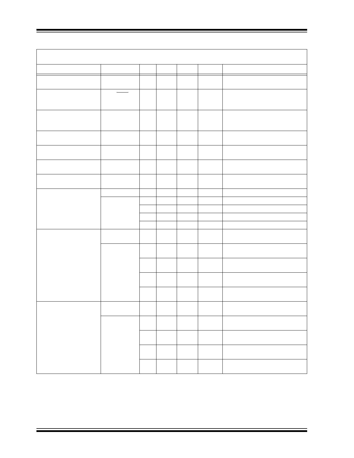
DC CHARACTERISTICS (CONTINUED)
Electrical Characteristics: Unless otherwise indicated, V
IN
= 1.2V, C
OUT
= C
IN
= 10 µF, L = 4.7 µH, V
OUT
= 3.3V,
I
OUT
= 15 mA, T
A
= +25°C, MCP1642B/D-ADJ. Boldface specifications apply over the T
A
range of -40
°
C to +85
°
C.
Parameters
Sym.
Min.
Typ.
Max.
Units
Conditions
Note 1:
Resistive load, 1 mA.
2:
For V
IN
> V
OUT
, V
OUT
will not remain in regulation.
3:
I
QPWM
is measured from V
OUT
; V
OUT
is externally supplied with a voltage higher than the nominal 3.3V
output (device is not switching), no load. V
IN
quiescent current will vary with boost ratio. V
IN
quiescent
current can be estimated by: (I
QPWM
* (V
OUT
/V
IN
)).
4:
220
resistive load, 3.3V V
OUT
(15 mA).
5:
Determined by characterization, not production tested.
2014 Microchip Technology Inc.
DS20005253A-page 5
MCP1642B/D
Maximum Duty Cycle
DC
MAX
—
90
—
%
Note 5
Switching Frequency
f
SW
0.85
1.0
1.15
MHz
Note 5
, I
OUT
= 65 mA,
for MCP1642B/D-50 V
IN
= 2.5V
EN Input Logic High
V
IH
75
—
—
% of V
IN
I
OUT
= 1 mA,
for MCP1642B/D-50 V
IN
= 2.5V
EN Input Logic Low
V
IL
—
—
20
% of V
IN
I
OUT
= 1 mA,
for MCP1642B/D-50 V
IN
= 2.5V
EN Input Leakage Current
I
ENLK
—
0.1
—
µA
V
EN
= 1.2V
Power Good Threshold
PG
THF
—
90
—
%
V
FB
Falling,
Note 5
Power Good Hysteresis
PG
HYS
—
3
—
%
Note 5
Power Good Output Low
PG
LOW
—
0.4
—
V
I
SINK
= 5 mA, V
FB
= 0V,
Note 5
Power Good Output Delay
PG
DELAY
—
600
—
µs
Note 5
Power Good Output
Response
PG
RES
—
250
—
µs
Note 5
Power Good Input Voltage
Operating Range
V
PG_VIN
0.9
—
5.5
V
I
SINK
= 5 mA, V
FB
= 0V,
Note 5
Power Good
Leakage Current
PG
LEAK
—
0.01
—
µA
V
PG
= 5.5V,
V
OUT
in Regulation,
Note 5
Soft Start Time
t
SS
—
550
—
µs
EN Low to High,
90% of V
OUT
,
Note 4
,
Note 5
Thermal Shutdown
Die Temperature
T
SD
—
150
—
C
Note 5
Die Temperature
Hysteresis
T
SDHYS
—
35
—
C
Note 5
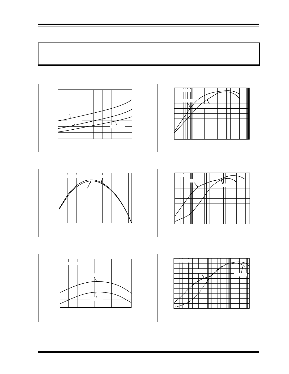
TEMPERATURE SPECIFICATIONS
Electrical Characteristics: Unless otherwise indicated, V
IN
= 1.2V, C
OUT
= C
IN
= 10 µF, L = 4.7 µH, V
OUT
= 3.3V,
I
OUT
= 15 mA, T
A
= +25°C.
Parameters
Sym.
Min.
Typ.
Max.
Units
Conditions
Temperature Ranges
Operating Ambient Temperature
Range
T
A
-40
—
+85
°C
Steady State
Storage Temperature Range
T
A
-65
—
+150
°C
Maximum Junction Temperature
T
J
—
—
+150
°C
Transient
Package Thermal Resistances
Thermal Resistance, 8L-MSOP
JA
—
211
—
°C/W
Thermal Resistance, 8L-2x3 DFN
JA
—
68
—
°C/W
DC CHARACTERISTICS (CONTINUED)
Electrical Characteristics: Unless otherwise indicated, V
IN
= 1.2V, C
OUT
= C
IN
= 10 µF, L = 4.7 µH, V
OUT
= 3.3V,
I
OUT
= 15 mA, T
A
= +25°C, MCP1642B/D-ADJ. Boldface specifications apply over the T
A
range of -40
°
C to +85
°
C.
Parameters
Sym.
Min.
Typ.
Max.
Units
Conditions
Note 1:
Resistive load, 1 mA.
2:
For V
IN
> V
OUT
, V
OUT
will not remain in regulation.
3:
I
QPWM
is measured from V
OUT
; V
OUT
is externally supplied with a voltage higher than the nominal 3.3V
output (device is not switching), no load. V
IN
quiescent current will vary with boost ratio. V
IN
quiescent
current can be estimated by: (I
QPWM
* (V
OUT
/V
IN
)).
4:
220
resistive load, 3.3V V
OUT
(15 mA).
5:
Determined by characterization, not production tested.

MCP1642B/D
DS20005253A-page 6
2014 Microchip Technology Inc.
NOTES:
2014 Microchip Technology Inc.
DS20005253A-page 7
MCP1642B/D
2.0
TYPICAL PERFORMANCE CURVES
Note: Unless otherwise indicated, V
IN
= EN = 1.2V, C
OUT
= C
IN
= 10 µF, L = 4.7 µH, V
OUT
= 3.3V, I
LOAD
= 15 mA,
T
A
= +25°C (MCP1642B/D-ADJ, MSOP-8 package).
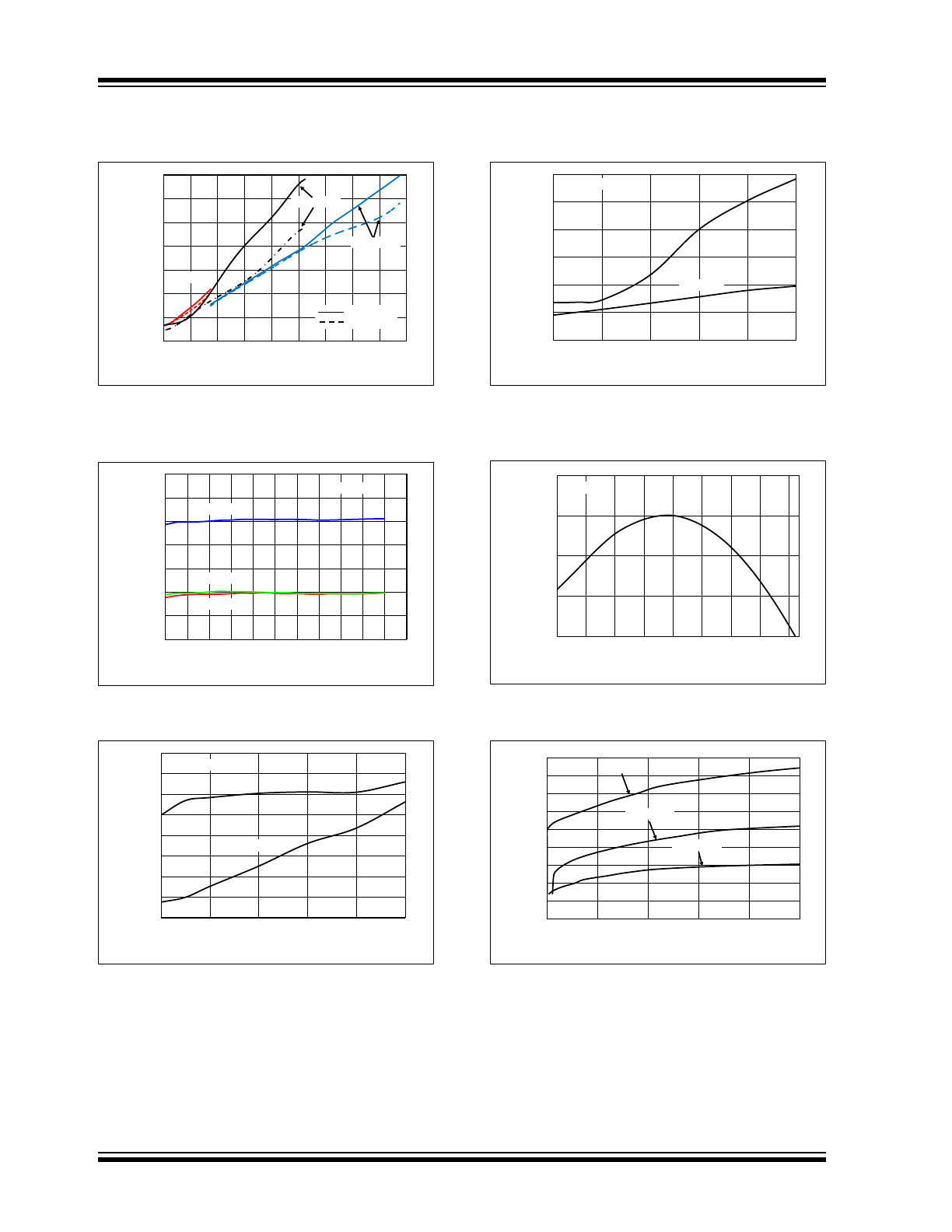
FIGURE 2-1:
V
OUT
I
QPWM
vs. Ambient
Temperature.
FIGURE 2-2:
3.3V V
OUT
vs. Ambient
Temperature.
FIGURE 2-3:
5.0V V
OUT
vs. Ambient
Temperature.
FIGURE 2-4:
2.0V V
OUT
Mode Efficiency
vs. I
OUT
.
FIGURE 2-5:
3.3V V
OUT
Mode Efficiency
vs. I
OUT
.
FIGURE 2-6:
5.0V V
OUT
Mode Efficiency
vs. I
OUT
.
Note:
The graphs and tables provided following this note are a statistical summary based on a limited number of
samples and are provided for informational purposes only. The performance characteristics listed herein
are not tested or guaranteed. In some graphs or tables, the data presented may be outside the specified
operating range (e.g., outside specified power supply range) and therefore outside the warranted range.
300
325
350
375
400
425
450
475
500
-40
-25
-10
5
20
35
50
65
80
I
Q
PWM Mode (µA)
Ambient Temperature (°C)
V
OUT
= 3.3V
V
OUT
= 5.0V
V
IN
= 1.2V
V
OUT
= 2.0V
3.304
3.306
3.308
3.310
3.312
3.314
-40
-25
-10
5
20
35
50
65
80
V
OUT
(V)
Ambient Temperature (°C)
I
OUT
= 50 mA
V
IN
= 1.8V
V
IN
= 1.2V
4.980
4.985
4.990
4.995
5.000
5.005
5.010
-40
-25
-10
5
20
35
50
65
80
V
OUT
(V)
Ambient Temperature (°C)
V
IN
= 2.5V
I
OUT
= 50 mA
V
IN
= 1.8V
0
10
20
30
40
50
60
70
80
90
100
0.1
1
10
100
1000
Efficiency
(%
)
I
OUT
(mA)
V
OUT
= 2.0V
V
IN
= 1.2V
V
IN
= 1.6V
0
10
20
30
40
50
60
70
80
90
100
0.1
1
10
100
1000
Efficiency
(%
)
I
OUT
(mA)
V
OUT
= 3.3V
V
IN
= 1.2V
V
IN
= 2.5V
0
10
20
30
40
50
60
70
80
90
100
0.1
1
10
100
1000
Efficiency
(%
)
I
OUT
(mA)
V
OUT
= 5.0V
V
IN
= 2.5V
V
IN
= 3.6V
MCP1642B/D
DS20005253A-page 8
2014 Microchip Technology Inc.
Note: Unless otherwise indicated, V
IN
= EN = 1.2V, C
OUT
= C
IN
= 10 µF, L = 4.7 µH, V
OUT
= 3.3V, I
LOAD
= 15 mA,
T
A
= +25°C (MCP1642B/D-ADJ, MSOP-8 package).
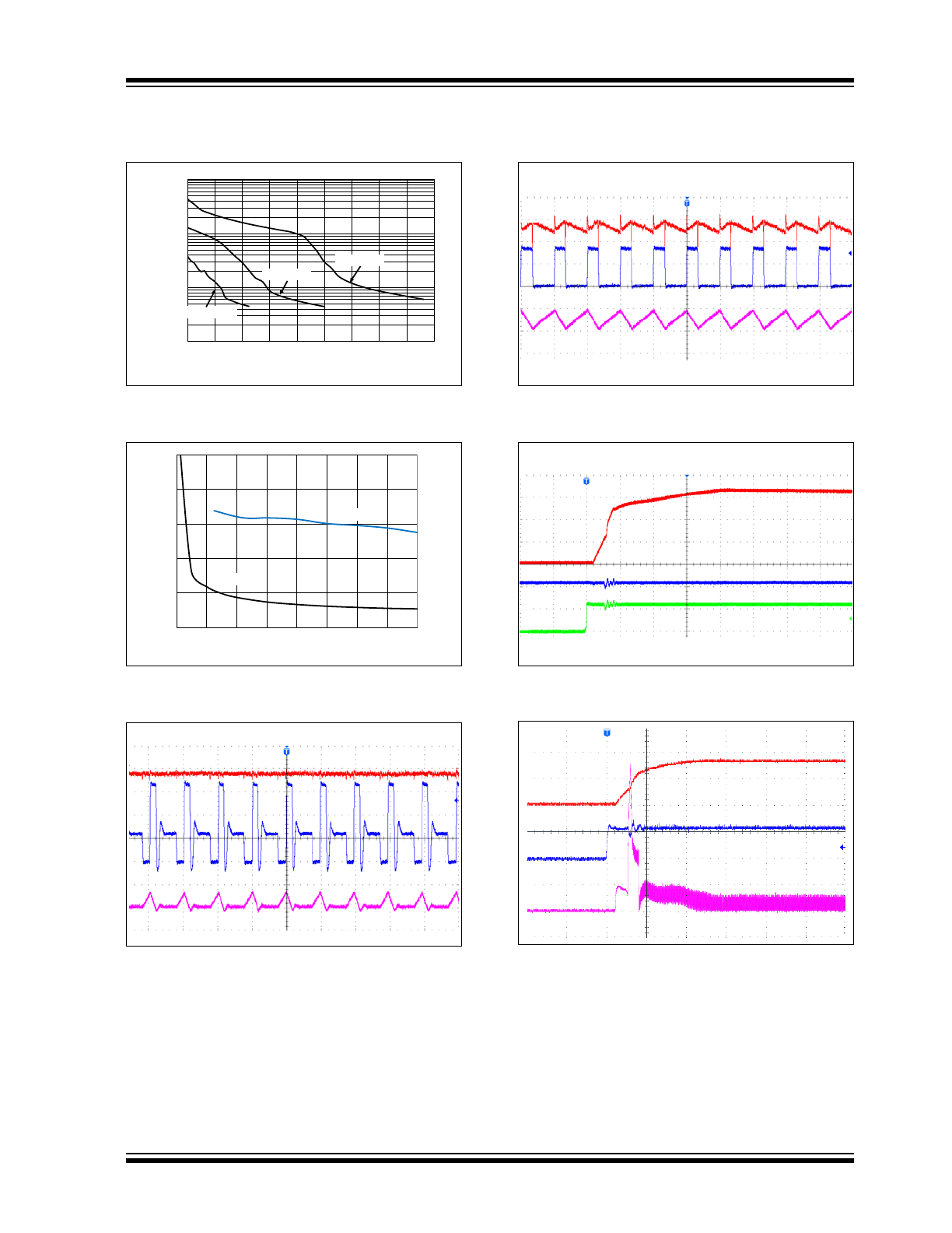
FIGURE 2-7:
Maximum I
OUT
vs. V
IN
.
FIGURE 2-8:
3.3V V
OUT
vs. V
IN
.
FIGURE 2-9:
3.3V V
OUT
Minimum
Start-Up and Shutdown V
IN
into Resistive Load
vs. I
OUT
.
FIGURE 2-10:
5.0V V
OUT
Minimum
Start-Up and Shutdown V
IN
into Resistive Load
vs. I
OUT
.
FIGURE 2-11:
f
SW
vs. Ambient
Temperature.
FIGURE 2-12:
PWM Pulse-Skipping Mode
Threshold vs. I
OUT
.
0
200
400
600
800
1000
1200
1400
0.8 1.2 1.6 2 2.4 2.8 3.2 3.6 4 4.4
I
OUT
(mA)
V
IN
(V)
V
OUT
= 3.3V
V
OUT
= 2.0V
V
OUT
= 5.0V
T
A
= +25
°C
T
A
= +85
°C
3.290
3.292
3.294
3.296
3.298
3.300
3.302
3.304
0.8
1 1.2 1.4 1.6 1.8
2 2.2 2.4 2.6 2.8
3
V
OUT
(V)
V
IN
(V)
T
A
= -40°C
I
OUT
= 15 mA
T
A
=
25°C
T
A
=
85°C
0.30
0.35
0.40
0.45
0.50
0.55
0.60
0.65
0.70
0
20
40
60
80
100
V
IN
(V)
I
OUT
(mA)
Start-up
Shutdown
V
OUT
= 3.3V
0.30
0.50
0.70
0.90
1.10
1.30
1.50
0
20
40
60
80
100
V
IN
(V)
I
OUT
(mA)
Start-up
Shutdown
V
OUT
= 5.0V
988
992
996
1000
1004
-40
-25
-10
5
20
35
50
65
80
Sw
itching Frequency
(kHz)
Ambient Temperature (°C)
V
OUT
= 3.3V
0
0.5
1
1.5
2
2.5
3
3.5
4
4.5
0
5
10
15
20
25
V
IN
(V)
I
OUT
(mA)
V
OUT
= 3.3V
V
OUT
= 5.0V
V
OUT
= 2.0V
2014 Microchip Technology Inc.
DS20005253A-page 9
MCP1642B/D
Note: Unless otherwise indicated, V
IN
= EN = 1.2V, C
OUT
= C
IN
= 10 µF, L = 4.7 µH, V
OUT
= 3.3V, I
LOAD
= 15 mA,
T
A
= +25°C (MCP1642B/D-ADJ, MSOP-8 package).
FIGURE 2-13:
Average of No Load Input
Current vs. V
IN
.
FIGURE 2-14:
N-Channel and P-Channel
R
DSON
vs. > of V
IN
or V
OUT
.
FIGURE 2-15:
MCP1642B/D 3.3V V
OUT
Light Load PWM Mode Waveforms.
FIGURE 2-16:
MCP1642B/D High Load
PWM Mode Waveforms.
FIGURE 2-17:
3.3V Start-Up After Enable.
FIGURE 2-18:
3.3V Start-Up When
V
IN
= V
ENABLE
.
0.1
1
10
100
0.8
1.2
1.6
2
2.4
2.8
3.2
3.6
4
4.4
I
IN
(mA)
V
IN
(V)
V
OUT
= 2.0V
V
OUT
= 3.3V
V
OUT
= 5.0V
0
0.05
0.1
0.15
0.2
0.25
0
0.5
1
1.5
2
2.5
1
1.4
1.8
2.2
2.6
3
3.4
3.8
4.2
Sw
itch Resistance
(:
)
> V
IN
or V
OUT
P - Channel
N - Channel
I
OUT
= 1 mA
1 µs/div
V
OUT
20 mV/div
AC coupled
I
L
V
SW
1V/div
100 mA/div
I
OUT
= 100 mA
V
SW
I
L
1 µs/div
V
OUT
20 mV/div
AC coupled
2V/div
200 mA/div
I
OUT
= 15 mA
V
OUT
1V/div
V
EN
1V/div
200 µs/div
V
IN
1V/div
I
L
200 mA/div
2V/div
V
OUT
200 µs/div
1V/div
V
IN
I
= 15 mA
OUT
MCP1642B/D
DS20005253A-page 10
2014 Microchip Technology Inc.
Note: Unless otherwise indicated, V
IN
= EN = 1.2V, C
OUT
= C
IN
= 10 µF, L = 4.7 µH, V
OUT
= 3.3V, I
LOAD
= 15 mA,
T
A
= +25°C (MCP1642B/D-ADJ, MSOP-8 package).
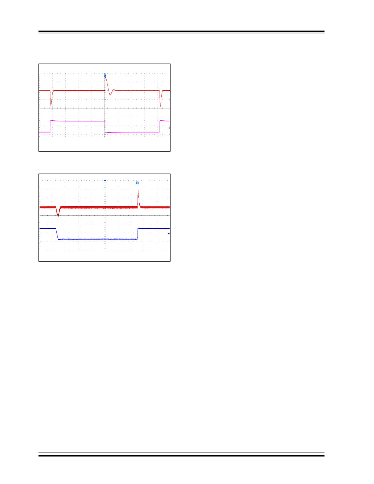
FIGURE 2-19:
MCP1642B 3.3V V
OUT
Load
Transient Waveforms.
FIGURE 2-20:
3.3V V
OUT
Line Transient
Waveforms.
I
OUT
100 mA/div
Step from 20 mA to 150 mA
400 µs/div
V
OUT
100 mV/div
AC coupled
V
IN
1V/div
Step from 1.2V to 2.4V
400 µs/div
V
OUT
100 mV/div
AC coupled
