
2010-2015 Microchip Technology Inc.
DS20002234D-page 1
MCP1640/B/C/D
Features
• Up to 96% Typical Efficiency
• 800 mA Typical Peak Input Current Limit:
- I
OUT
> 100 mA @ 1.2V V
IN
, 3.3V V
OUT
- I
OUT
> 350 mA @ 2.4V V
IN
, 3.3V V
OUT
- I
OUT
> 350 mA @ 3.3V V
IN
, 5.0V V
OUT
• Low Start-Up Voltage: 0.65V, typical 3.3V V
OUT
@ 1 mA
• Low Operating Input Voltage: 0.35V, typical
3.3V
OUT
@ 1 mA
• Adjustable Output Voltage Range: 2.0V to 5.5V
• Maximum Input Voltage
V
OUT
< 5.5V
• Automatic PFM/PWM Operation (MCP1640/C):
- PFM Operation Disabled (MCP1640B/D)
- PWM Operation: 500 kHz
• Low Device Quiescent Current: 19 µA, typical
PFM Mode (not switching)
• Internal Synchronous Rectifier
• Internal Compensation
• Inrush Current Limiting and Internal Soft Start
• Selectable, Logic Controlled Shutdown States:
- True Load Disconnect Option (MCP1640/B)
- Input to Output Bypass Option (MCP1640C/D)
• Shutdown Current (All States): < 1 µA
• Low Noise, Anti-Ringing Control
• Overtemperature Protection
• Available Packages:
- 6-Lead SOT-23
- 8-Lead 2 x 3 mm DFN
Applications
• One, Two and Three Cell Alkaline and NiMH/NiCd
Portable Products
• Single-Cell Li-Ion to 5V Converters
• Li Coin Cell Powered Devices
• Personal Medical Products
• Wireless Sensors
• Handheld Instruments
• GPS Receivers
• Bluetooth Headsets
• +3.3V to +5.0V Distributed Power Supply
General Description
The MCP1640/B/C/D is a compact, high-efficiency,
fixed frequency, synchronous step-up DC-DC con-
verter. It provides an easy-to-use power supply solution
for applications powered by either single-cell, two-cell,
or three-cell alkaline, NiCd, NiMH, and single-cell Li-Ion
or Li-Polymer batteries.
Low-voltage technology allows the regulator to start-up
without high inrush current or output voltage overshoot
from a low 0.65V input. High efficiency is accomplished
by integrating the low resistance N-Channel Boost
switch and synchronous P-Channel switch. All
compensation and protection circuitry is integrated to
minimize the number of external components. For
standby applications, the MCP1640 consumes only
19 µA while operating at no load, and provides a true
disconnect from input to output while in Shutdown
(EN = GND). Additional device options are available by
operating in PWM-Only mode and connecting input to
output while the device is in Shutdown.
The “true” load disconnect mode provides input-to-out-
put isolation while the device is disabled by removing
the normal boost regulator diode path from input-to-
output. The Input-to-Output Bypass mode option con-
nects the input to the output using the integrated low
resistance P-Channel MOSFET, which provides a low
bias voltage for circuits operating in Deep Sleep mode.
Both options consume less than 1 µA of input current.
Output voltage is set by a small external resistor
divider. Two package options are available, 6-Lead
SOT-23 and 8-Lead 2 x 3 mm DFN.
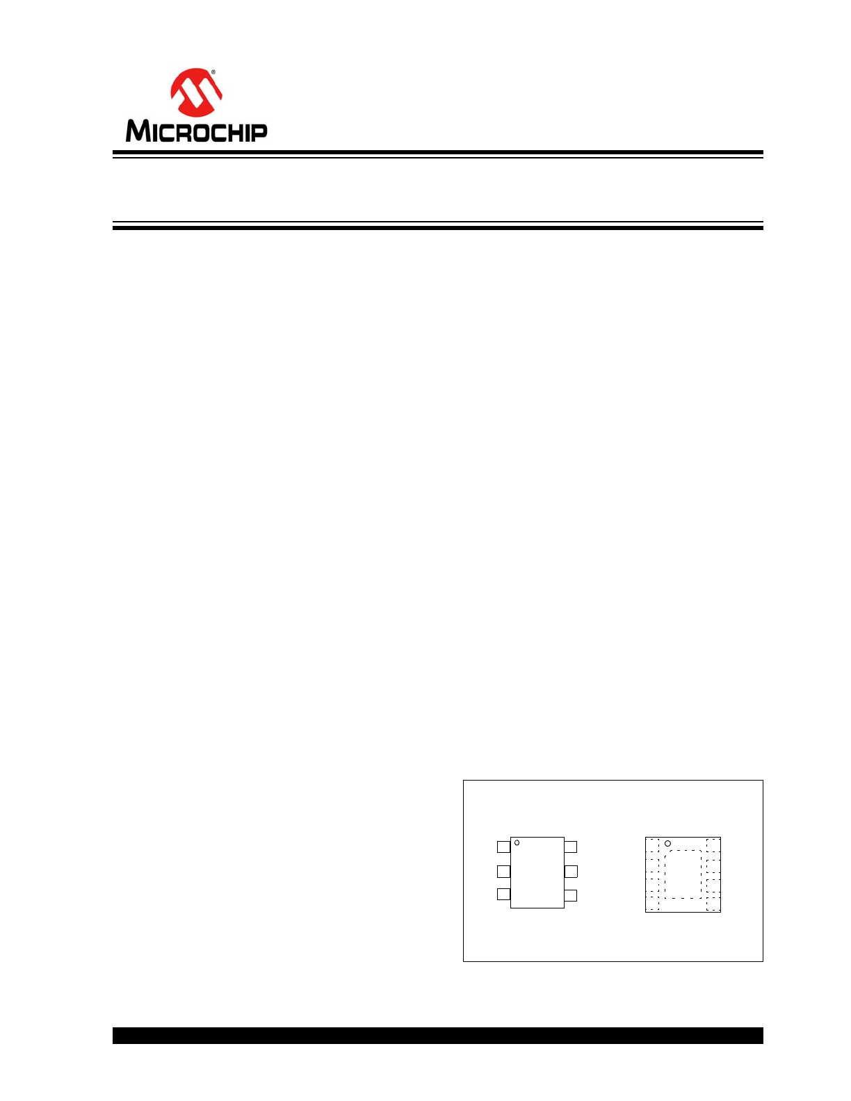
Package Types
MCP1640
8-Lead 2 x 3 DFN*
P
GND
S
GND
EN
V
OUTS
V
OUTP
1
2
3
4
8
7
6
5 SW
V
IN
V
FB
EP
9
4
1
2
3
6 V
IN
V
FB
SW
GND
EN
5 V
OUT
MCP1640
6-Lead SOT-23
* Includes Exposed Thermal Pad (EP); see
Table 3-1
.
0.65V Start-Up Synchronous Boost Regulator
with True Output Disconnect or Input/Output Bypass Option
MCP1640/B/C/D
DS20002234D-page 2
2010-2015 Microchip Technology Inc.
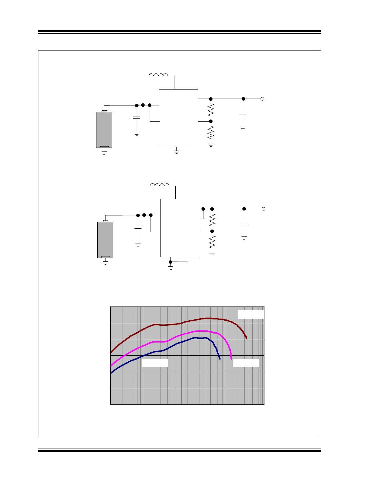
Typical Application
Efficiency vs. I
OUT
for 3.3V
OUT
40.0
60.0
80.0
100.0
0.1
1.0
10.0
100.0
1000.0
Output Current (mA)
E
ffi
ci
e
n
cy
(%
)
V
IN
= 0.8V
V
IN
= 1.2V
V
IN
= 2.5V
V
IN
GND
V
FB
SW
V
IN
0.9V to 1.7V
V
OUT
3.3V @ 100 mA
C
OUT
10 µF
C
IN
4.7 µF
L
1
4.7 µH
V
OUT
+
-
976 k
562 k
AL
KAL
IN
E
V
IN
P
GND
V
FB
SW
V
IN
3.0V to 4.2V
V
OUT
5.0V @ 300 mA
C
OUT
10 µF
C
IN
4.7 µF
L
1
4.7 µH
V
OUTS
+
-
976 k
309 k
V
OUTP
S
GND
LI-
ION
EN
EN
2010-2015 Microchip Technology Inc.
DS20002234D-page 3
MCP1640/B/C/D
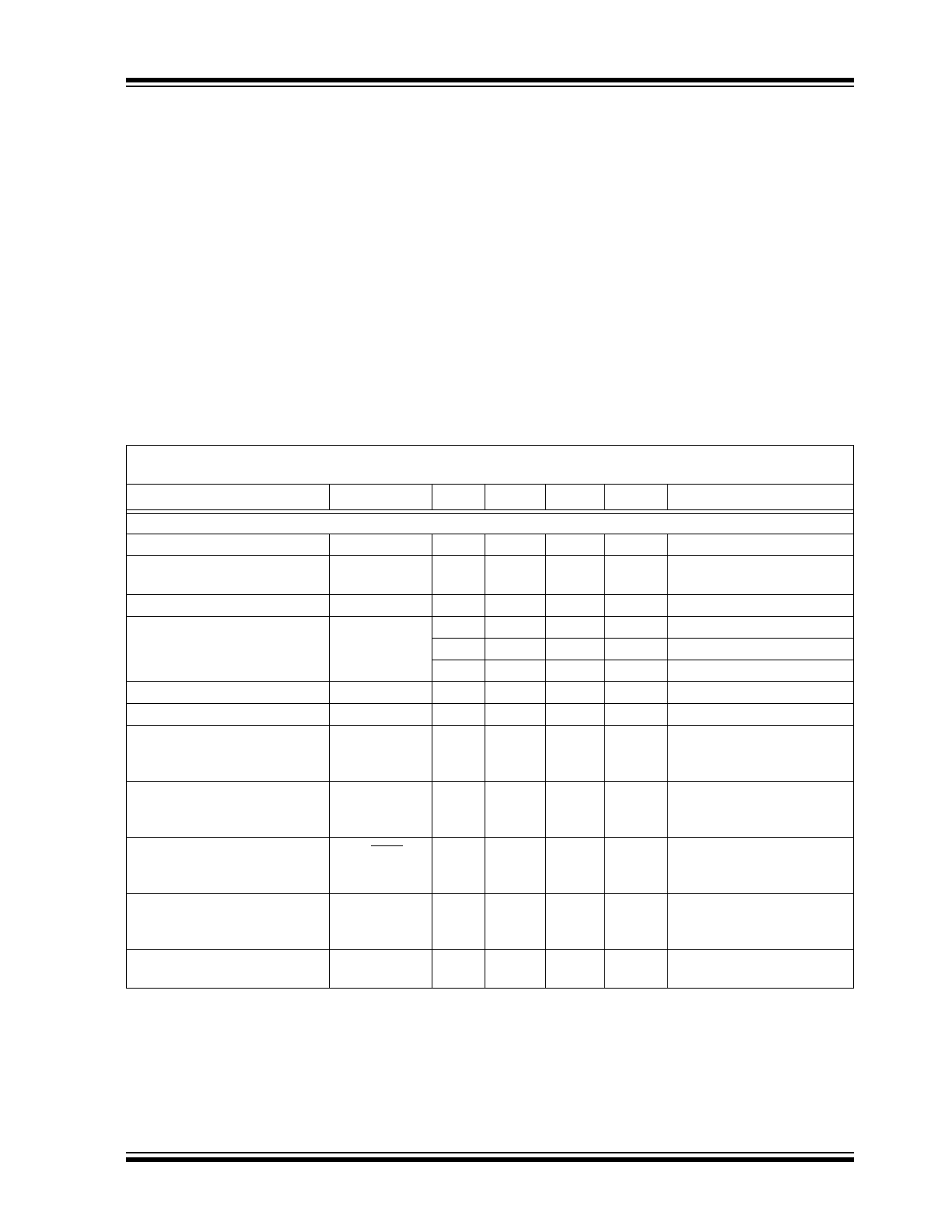
1.0
ELECTRICAL
CHARACTERISTICS
Absolute Maximum Ratings †
EN, V
FB
, V
IN,
V
SW
, V
OUT
- GND ......................... +6.5V
EN, V
FB
.... <maximum of V
OUT
or V
IN
> (GND – 0.3V)
Output Short-Circuit Current ...................... Continuous
Output Current Bypass Mode........................... 400 mA
Power Dissipation ............................ Internally Limited
Storage Temperature ......................... -65°C to +150°C
Ambient Temp. with Power Applied...... -40°C to +85°C
Operating Junction Temperature........ -40°C to +125°C
ESD Protection On All Pins:
HBM........................................................ 3 kV
MM......................................................... 300V
† Notice: Stresses above those listed under “Maximum
Ratings” may cause permanent damage to the device.
This is a stress rating only and functional operation of
the device at those or any other conditions above those
indicated in the operational sections of this
specification is not intended. Exposure to maximum
rating conditions for extended periods may affect
device reliability.
DC CHARACTERISTICS
Electrical Characteristics: Unless otherwise indicated, V
IN
= 1.2V, C
OUT
= C
IN
= 10 µF, L = 4.7 µH, V
OUT
= 3.3V,
I
OUT
= 15 mA, T
A
= +25°C. Boldface specifications apply over the T
A
range of -40°C to +85°C.
Parameters
Sym.
Min.
Typ.
Max.
Units
Conditions
Input Characteristics
Minimum Start-Up Voltage
V
IN
—
0.65
0.8
V
Note 1
Minimum Input Voltage After
Start-Up
V
IN
—
0.35
—
V
Note 1
Output Voltage Adjust Range
V
OUT
2.0
5.5
V
V
OUT
V
IN
;
Note 2
Maximum Output Current
I
OUT
—
150
—
mA
1.2V V
IN
, 2.0V V
OUT
—
150
—
mA
1.5V V
IN
, 3.3V V
OUT
—
350
—
mA
3.3V V
IN
, 5.0V V
OUT
Feedback Voltage
V
FB
1.175
1.21
1.245
V
Feedback Input Bias Current
I
VFB
—
10
—
pA
Quiescent Current – PFM
Mode
I
QPFM
—
19
30
µA
Measured at V
OUT
= 4.0V;
EN = V
IN
, I
OUT
= 0 mA;
Note 3
Quiescent Current – PWM
Mode
I
QPWM
—
220
—
µA
Measured at V
OUT
= 4.0V;
EN = V
IN,
I
OUT
= 0 mA;
Note 3
Quiescent Current – Shutdown
I
QSHDN
—
0.7
2.3
µA
V
OUT
= EN = GND;
Includes N-Channel and
P-Channel Switch Leakage
NMOS Switch Leakage
I
NLK
—
0.3
—
µA
V
IN
= V
SW
= 5V;
V
OUT
= 5.5V
V
EN
= V
FB
= GND
PMOS Switch Leakage
I
PLK
—
0.05
—
µA
V
IN
= VS
W
= GND;
V
OUT
= 5.5V
Note 1:
3.3 k
resistive load, 3.3V
OUT
(1 mA).
2:
For V
IN
> V
OUT
, V
OUT
will not remain in regulation.
3:
I
QOUT
is measured at V
OUT
; V
OUT
is externally supplied with a voltage higher than the nominal 3.3V output
(device is not switching); no load; V
IN
quiescent current will vary with boost ratio. V
IN
quiescent current
can be estimated by: (I
QPFM
* (V
OUT
/V
IN
)), (I
QPWM
* (V
OUT
/V
IN
)).
4:
Peak current limit determined by characterization, not production tested.
5:
220
resistive load, 3.3V
OUT
(15 mA).
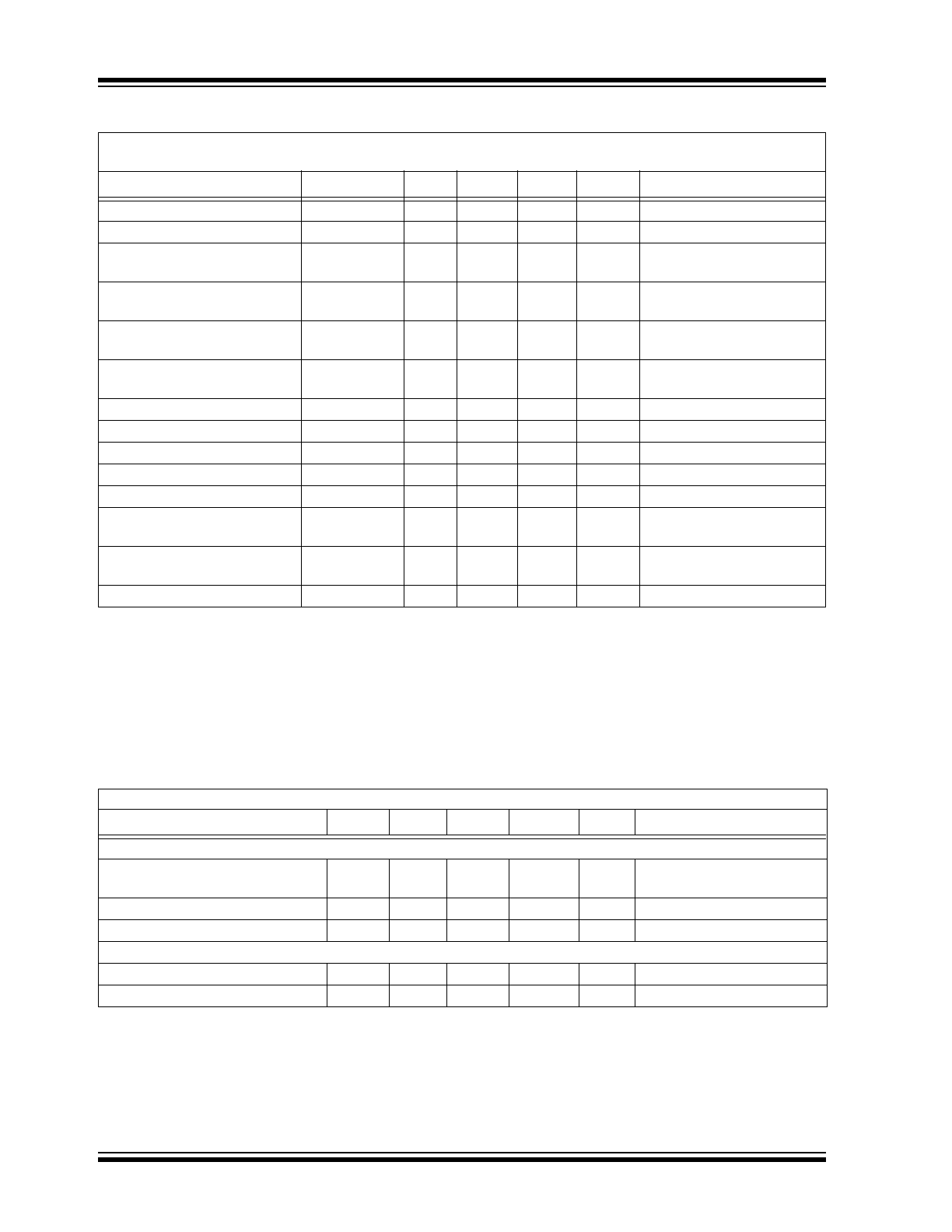
MCP1640/B/C/D
DS20002234D-page 4
2010-2015 Microchip Technology Inc.
NMOS Switch On Resistance
R
DS(ON)N
—
0.6
—
V
IN
= 3.3V, I
SW
= 100 mA
PMOS Switch On Resistance
R
DS(ON)P
—
0.9
—
V
IN
= 3.3V, I
SW
= 100 mA
NMOS Peak Switch Current
Limit
I
N(MAX)
600
850
—
mA
Note 4
V
OUT
Accuracy
V
OUT
%
-3
—
+3
%
Includes Line and Load
Regulation; V
IN
= 1.5V
Line Regulation
V
OUT
/V
OUT
)
/
V
IN
|
-1
0.01
1
%/V
V
IN
= 1.5V to 3V
I
OUT
= 25 mA
Load Regulation
V
OUT
/V
OUT
|
-1
0.01
1
%
I
OUT
= 25 mA to 100 mA;
V
IN
= 1.5V
Maximum Duty Cycle
DC
MAX
88
90
—
%
Switching Frequency
f
SW
425
500
575
kHz
EN Input Logic High
V
IH
90
—
—
%of V
IN
I
OUT
= 1 mA
EN Input Logic Low
V
IL
—
—
20
%of V
IN
I
OUT
= 1 mA
EN Input Leakage Current
I
ENLK
—
0.005
—
µA
V
EN
= 5V
Soft-Start Time
t
SS
—
750
—
µS
EN Low-to-High,
90% of V
OUT
;
Note 5
Thermal Shutdown Die
Temperature
T
SD
—
150
—
C
Die Temperature Hysteresis
T
SDHYS
—
10
—
C
TEMPERATURE SPECIFICATIONS
Electrical Specifications: Unless otherwise indicated, V
IN
= 1.2V, C
OUT
= C
IN
= 10 µF, L = 4.7 µH, V
OUT
= 3.3V, I
OUT
= 15 mA.
Parameters
Sym.
Min.
Typ.
Max.
Units
Conditions
Temperature Ranges
Operating Junction Temperature
Range
T
J
-40
—
+125
°C
Steady State
Storage Temperature Range
T
A
-65
—
+150
°C
Maximum Junction Temperature
T
J
—
—
+150
°C
Transient
Package Thermal Resistances
Thermal Resistance, 6LD-SOT-23
JA
—
190.5
—
°C/W
Thermal Resistance, 8LD-2x3 DFN
JA
—
75
—
°C/W
DC CHARACTERISTICS (CONTINUED)
Electrical Characteristics: Unless otherwise indicated, V
IN
= 1.2V, C
OUT
= C
IN
= 10 µF, L = 4.7 µH, V
OUT
= 3.3V,
I
OUT
= 15 mA, T
A
= +25°C. Boldface specifications apply over the T
A
range of -40°C to +85°C.
Parameters
Sym.
Min.
Typ.
Max.
Units
Conditions
Note 1:
3.3 k
resistive load, 3.3V
OUT
(1 mA).
2:
For V
IN
> V
OUT
, V
OUT
will not remain in regulation.
3:
I
QOUT
is measured at V
OUT
; V
OUT
is externally supplied with a voltage higher than the nominal 3.3V output
(device is not switching); no load; V
IN
quiescent current will vary with boost ratio. V
IN
quiescent current
can be estimated by: (I
QPFM
* (V
OUT
/V
IN
)), (I
QPWM
* (V
OUT
/V
IN
)).
4:
Peak current limit determined by characterization, not production tested.
5:
220
resistive load, 3.3V
OUT
(15 mA).
2010-2015 Microchip Technology Inc.
DS20002234D-page 5
MCP1640/B/C/D
2.0
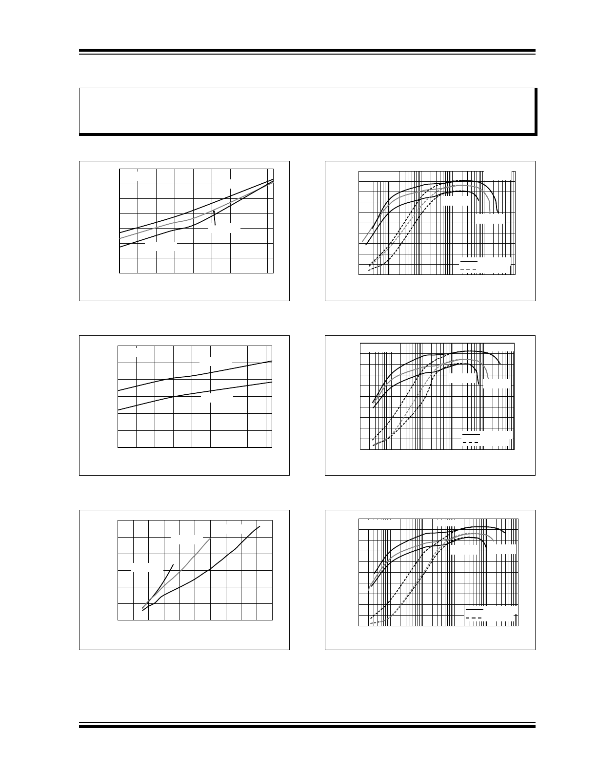
TYPICAL PERFORMANCE CURVES
Note: Unless otherwise indicated,
V
IN
= EN = 1.2V, C
OUT
= C
IN
= 10 µF, L
= 4.7 µH, V
OUT
= 3.3V, I
LOAD
= 15 mA, T
A
= +25°C.
FIGURE 2-1:
V
OUT
I
Q
vs. Ambient
Temperature in PFM Mode.
FIGURE 2-2:
V
OUT
I
Q
vs. Ambient
Temperature in PWM Mode.
FIGURE 2-3:
Maximum I
OUT
vs. V
IN
After
Start-Up, V
OUT
10% Below Regulation Point.
FIGURE 2-4:
2.0V V
OUT
PFM/PWM Mode
Efficiency vs. I
OUT
.
FIGURE 2-5:
3.3V V
OUT
PFM/PWM Mode
Efficiency vs. I
OUT
.
FIGURE 2-6:
5.0V V
OUT
PFM/PWM Mode
Efficiency vs. I
OUT
.
Note:
The graphs and tables provided following this note are a statistical summary based on a limited number of
samples and are provided for informational purposes only. The performance characteristics listed herein
are not tested or guaranteed. In some graphs or tables, the data presented may be outside the specified
operating range (e.g., outside specified power supply range) and therefore outside the warranted range.
10.0
12.5
15.0
17.5
20.0
22.5
25.0
27.5
-40
-25
-10
5
20
35
50
65
80
IQ PFM
Mode
(µA)
Ambient Temperature (°C)
V
OUT
= 2.0V
V
OUT
= 5.0V
V
OUT
= 3.3V
V
IN
= 1.2V
150
175
200
225
250
275
300
-40
-25
-10
5
20
35
50
65
80
I
Q
PWM Mode (µA)
Ambient Temperature (°C)
V
OUT
= 3.3V
V
OUT
= 5.0V
V
IN
= 1.2V
0
100
200
300
400
500
600
0
0.5
1
1.5
2
2.5
3
3.5
4
4.5
5
I
OUT
(mA)
V
IN
(V)
V
OUT
= 3.3V
V
OUT
= 2.0V
V
OUT
= 5.0V
0
10
20
30
40
50
60
70
80
90
100
0.01
0.1
1
10
100
1000
Efficiency
(%
)
I
OUT
(mA)
V
OUT
= 2.0V
V
IN
= 0.8V
V
IN
= 1.2V
V
IN
= 1.6V
PWM / PFM
PWM Only
0
10
20
30
40
50
60
70
80
90
100
0.01
0.1
1
10
100
1000
Efficiency
(%
)
I
OUT
(mA)
V
OUT
= 3.3V
V
IN
= 0.8V
V
IN
= 1.2V
V
IN
= 2.5V
PWM / PFM
PWM Only
0
10
20
30
40
50
60
70
80
90
100
0.01
0.1
1
10
100
1000
Efficiency
(%
)
I
OUT
(mA)
V
OUT
= 5.0V
V
IN
= 1.2V
V
IN
= 1.8V
V
IN
= 3.6V
PWM / PFM
PWM Only
MCP1640/B/C/D
DS20002234D-page 6
2010-2015 Microchip Technology Inc.
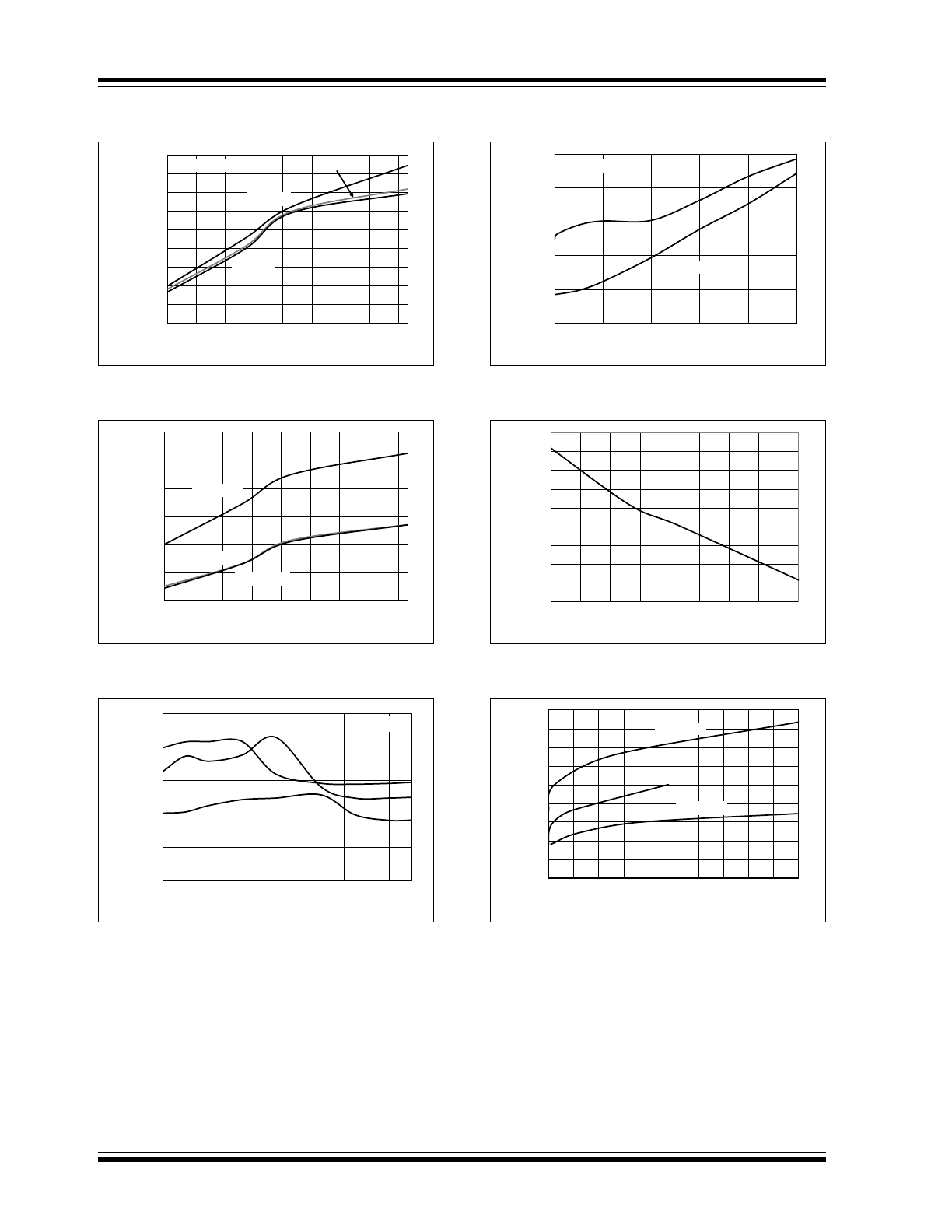
Note: Unless otherwise indicated,
V
IN
= EN = 1.2V, C
OUT
= C
IN
= 10 µF, L
= 4.7 µH, V
OUT
= 3.3V, I
LOAD
= 15 mA, T
A
= +25°C.
FIGURE 2-7:
3.3V V
OUT
vs. Ambient
Temperature.
FIGURE 2-8:
3.3V V
OUT
vs. Ambient
Temperature.
FIGURE 2-9:
3.3V V
OUT
vs. V
IN
.
FIGURE 2-10:
Minimum Start-Up and
Shutdown V
IN
into Resistive Load vs. I
OUT
.
FIGURE 2-11:
F
OSC
vs. Ambient
Temperature.
FIGURE 2-12:
PWM Pulse-Skipping Mode
Threshold vs. I
OUT
.
3.285
3.29
3.295
3.3
3.305
3.31
3.315
3.32
3.325
3.33
-40
-25
-10
5
20
35
50
65
80
V
OUT
(V)
Ambient Temperature (°C)
I
OUT
= 15 mA
V
IN
= 0.8V
V
IN
= 1.8V
V
IN
= 1.2V
3.26
3.28
3.30
3.32
3.34
3.36
3.38
-40
-25
-10
5
20
35
50
65
80
V
OUT
(V)
Ambient Temperature (°C)
I
OUT
= 15 mA
V
IN
= 1.5V
I
OUT
= 50 mA
I
OUT
= 5 mA
3.20
3.24
3.28
3.32
3.36
3.40
0.8
1.2
1.6
2
2.4
2.8
V
OUT
(V)
V
IN
(V)
T
A
= -40°C
I
OUT
= 5 mA
T
A
= +25°C
T
A
= +85°C
0.25
0.40
0.55
0.70
0.85
1.00
0
20
40
60
80
100
V
IN
(V)
I
OUT
(mA)
Startup
Shutdown
V
OUT
= 3.3V
480
485
490
495
500
505
510
515
520
525
-40
-25
-10
5
20
35
50
65
80
Sw
itching Frequency
(kHz)
Ambient Temperature (°C)
V
OUT
= 3.3V
0
0.5
1
1.5
2
2.5
3
3.5
4
4.5
0
1
2
3
4
5
6
7
8
9
10
V
IN
(V)
I
OUT
(mA)
V
OUT
= 3.3V
V
OUT
= 5.0V
V
OUT
= 2.0V
2010-2015 Microchip Technology Inc.
DS20002234D-page 7
MCP1640/B/C/D
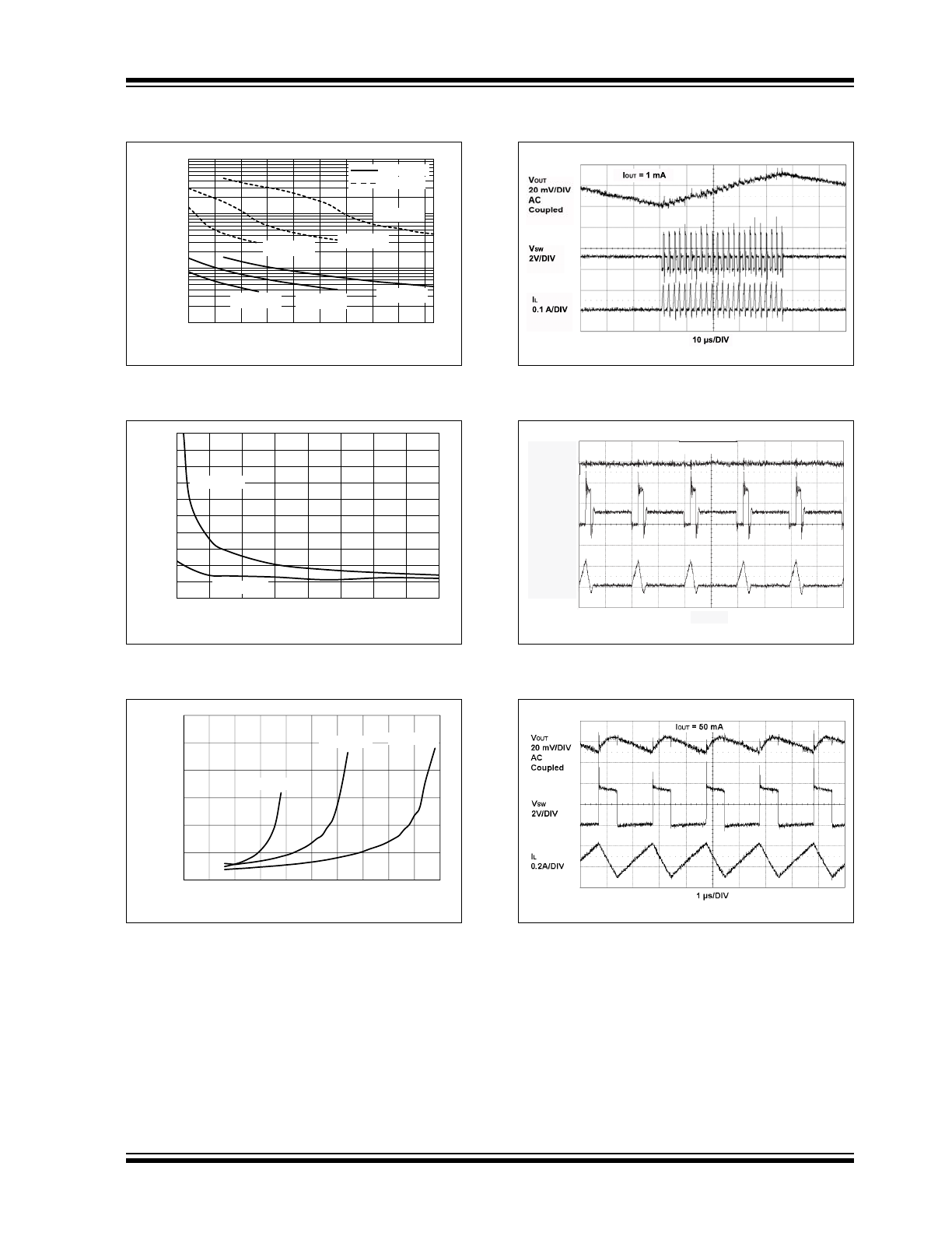
Note: Unless otherwise indicated,
V
IN
= EN = 1.2V, C
OUT
= C
IN
= 10 µF, L
= 4.7 µH, V
OUT
= 3.3V, I
LOAD
= 15 mA, T
A
= +25°C.
FIGURE 2-13:
Input No Load Current vs.
V
IN
.
FIGURE 2-14:
N-Channel and P-Channel
R
DSON
vs. > of V
IN
or V
OUT
.
FIGURE 2-15:
Average of PFM/PWM
Threshold Current vs. V
IN
.
FIGURE 2-16:
MCP1640 3.3V V
OUT
PFM
Mode Waveforms.
FIGURE 2-17:
MCP1640B 3.3V V
OUT
PWM Mode Waveforms.
FIGURE 2-18:
MCP1640/B High Load
Waveforms.
10
100
1000
10000
0.8
1.1
1.4
1.7
2
2.3
2.6
2.9
3.2
3.5
I
IN
(µA)
V
IN
(V)
V
OUT
= 3.3V
V
OUT
= 5.0V
V
OUT
= 2.0V
V
OUT
= 2.0V
V
OUT
= 3.3V
V
OUT
= 5.0V
PWM / PFM
PWM Only
0
1
2
3
4
5
1
1.5
2
2.5
3
3.5
4
4.5
5
Sw
itch Resistance
(Ohms)
> V
IN
or V
OUT
P - Channel
N - Channel
0
10
20
30
40
50
60
0
0.5
1
1.5
2
2.5
3
3.5
4
4.5
5
I
OUT
(mA)
V
IN
(V)
V
OUT
= 2.0V
V
OUT
= 3.3V
V
OUT
= 5.0V
I
OUT
= 1 mA
1 µs/DIV
V
OUT
20 mV/DIV
AC
Coupled
V
SW
2V/DIV
I
L
0.05 mA/DIV
MCP1640/B/C/D
DS20002234D-page 8
2010-2015 Microchip Technology Inc.
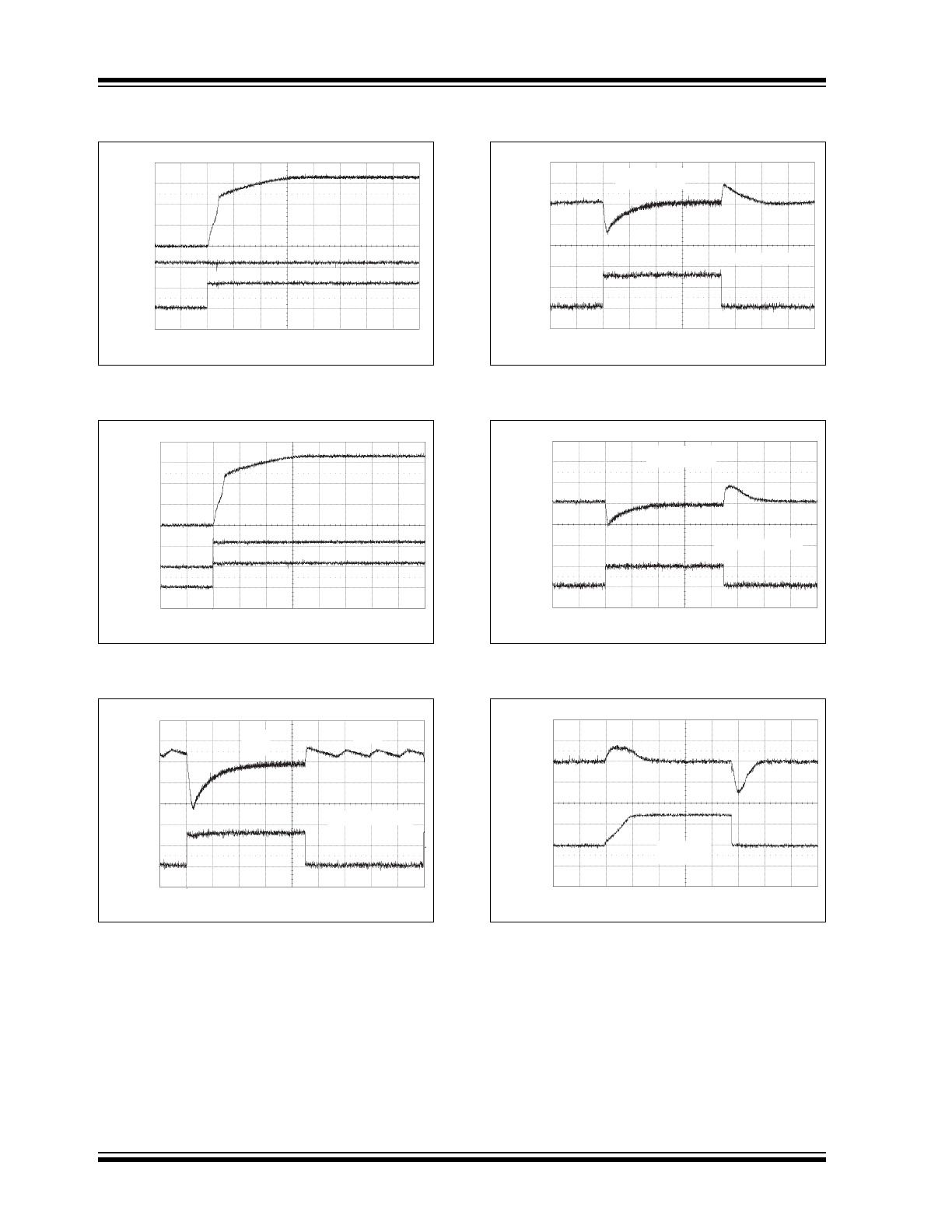
Note: Unless otherwise indicated,
V
IN
= EN = 1.2V, C
OUT
= C
IN
= 10 µF, L
= 4.7 µH, V
OUT
= 3.3V, I
LOAD
= 15 mA, T
A
= +25°C.
FIGURE 2-19:
3.3V Start-Up After Enable.
FIGURE 2-20:
3.3V Start-Up when
V
IN
= V
ENABLE
.
FIGURE 2-21:
MCP1640 3.3V V
OUT
Load
Transient Waveforms.
FIGURE 2-22:
MCP1640B 3.3V V
OUT
Load
Transient Waveforms.
FIGURE 2-23:
MCP1640B 2.0V V
OUT
Load
Transient Waveforms.
FIGURE 2-24:
3.3V V
OUT
Line Transient
Waveforms.
V
OUT
1V/DIV
V
IN
1V/DIV
V
EN
1V/DIV
500 µs/DIV
V
OUT
1V/DIV
V
IN
1V/DIV
V
EN
1V/DIV
500 µs/DIV
PFM
MODE
PWM
MODE
I
STEP
= 1 mA to 75 mA
V
OUT
100 mV/DIV
AC
Coupled
I
OUT
50 mA/DIV
100 µs/DIV
MCP1640B PWM
Mode Only
V
OUT
100 mV/DIV
AC
Coupled
I
OUT
50 mA/DIV
100 µs/DIV
I
STEP
= 1 mA to 75 mA
MCP1640B PWM
Mode Only
100 µs/DIV
V
OUT
50 mV/DIV
AC
Coupled
I
OUT
50 mA/DIV
I
STEP
= 1 mA to 50 mA
V
STEP
from
1V to 2.5V
200 µs/DIV
V
OUT
50 mV/DIV
AC
Coupled
V
IN
1V/DIV
2010-2015 Microchip Technology Inc.
DS20002234D-page 9
MCP1640/B/C/D
3.0
PIN DESCRIPTIONS
The descriptions of the pins are listed in
Table 3-1
.
3.1
Feedback Voltage Pin (V
FB
)
The V
FB
pin is used to provide output voltage regulation
by using a resistor divider. Feedback voltage will be
1.21V typical with the output voltage in regulation.
3.2
Signal Ground Pin (S
GND
)
The signal ground pin is used as a return for the
integrated V
REF
and error amplifier. In the 2x3 DFN
package, the S
GND
and power ground (P
GND
) pins are
connected externally.
3.3
Power Ground Pin (P
GND
)
The power ground pin is used as a return for the
high-current N-Channel switch. In the 2x3 DFN
package, the P
GND
and S
GND
pins are connected
externally.
3.4
Enable Pin (EN)
The EN pin is a logic-level input used to enable or
disable device switching and lower quiescent current
while disabled. A logic high (>90% of V
IN
) will enable
the regulator output. A logic low (<20% of V
IN
) will
ensure that the regulator is disabled.
3.5
Switch Node Pin (SW)
Connect the inductor from the input voltage to the SW
pin. The SW pin carries inductor current and can be as
high as 800 mA peak. The integrated N-Channel switch
drain and integrated P-Channel switch source are
internally connected at the SW node.
3.6
Output Voltage Power Pin (V
OUTP
)
The output voltage power pin connects the output
voltage to the switch node. High current flows through
the integrated P-Channel and out of this pin to the
output capacitor and the output. In the 2x3 DFN
package, V
OUTP
and V
OUTS
are connected externally.
3.7
Output Voltage Sense Pin (V
OUTS
)
The output voltage sense pin connects the regulated
output voltage to the internal bias circuits. In the
2x3 DFN package, the V
OUTS
and output voltage
power (V
OUTP
)
pins are connected externally.
3.8
Power Supply Input Voltage Pin (V
IN
)
Connect the input voltage source to V
IN
. The input
source should be decoupled to GND with a 4.7 µF
minimum capacitor.
3.9
Exposed Thermal Pad (EP)
There is no internal electrical connection between the
Exposed Thermal Pad (EP) and the S
GND
and P
GND
pins. They must be connected to the same potential on
the Printed Circuit Board (PCB).
3.10
Ground Pin (GND)
The ground or return pin is used for circuit ground
connection. Length of trace from input cap return,
output cap return, and GND pin should be made as
short as possible to minimize noise on the GND pin. In
the SOT-23-6 package, a single ground pin is used.
3.11
Output Voltage Pin (V
OUT
)
The output voltage pin connects the integrated
P-Channel MOSFET to the output capacitor. The FB
voltage divider is also connected to the V
OUT
pin for
voltage regulation.
TABLE 3-1:
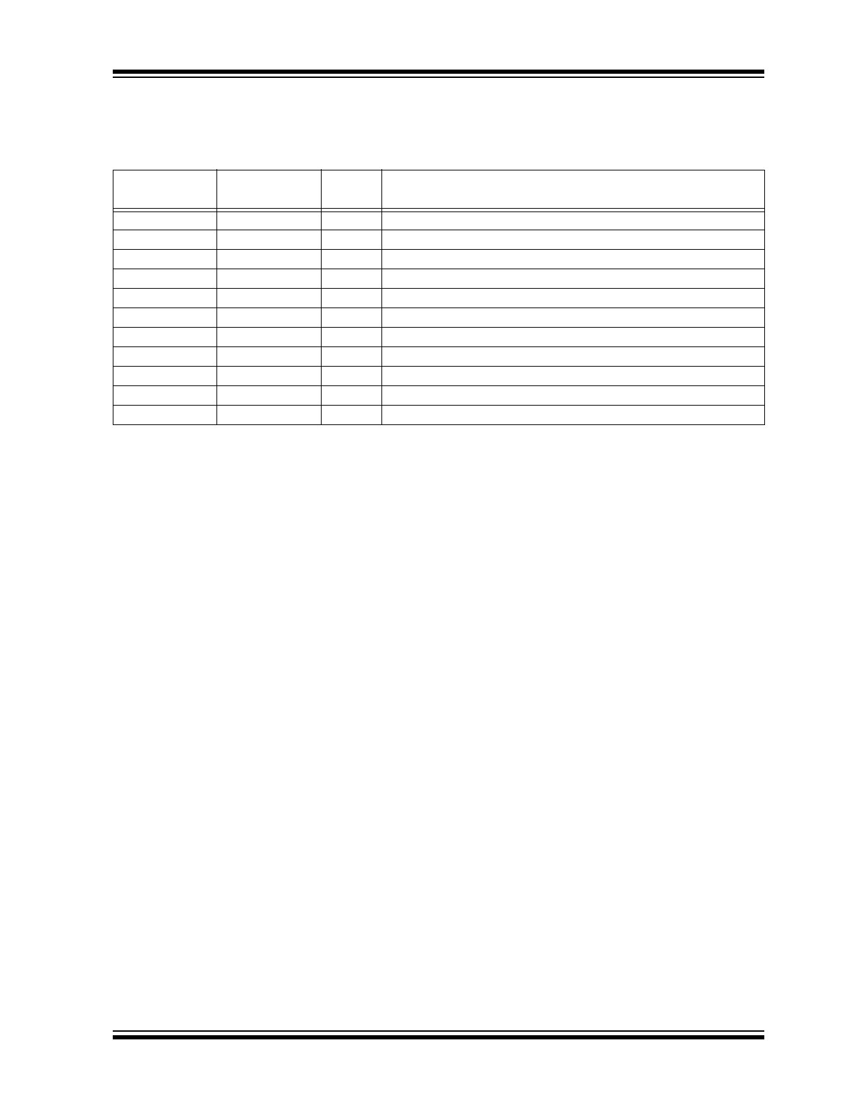
PIN FUNCTION TABLE
MCP1640/B/C/D
2x3 DFN
MCP1640/B/C/D
SOT-23
Symbol
Description
1
4
V
FB
Feedback Voltage Pin
2
—
S
GND
Signal Ground Pin
3
—
P
GND
Power Ground Pin
4
3
EN
Enable Control Input Pin
5
1
SW
Switch Node, Boost Inductor Input Pin
6
—
V
OUTP
Output Voltage Power Pin
7
—
V
OUTS
Output Voltage Sense Pin
8
6
V
IN
Input Voltage Pin
9
—
EP
Exposed Thermal Pad (EP); must be connected to V
SS
—
2
GND
Ground Pin
—
5
V
OUT
Output Voltage Pin

MCP1640/B/C/D
DS20002234D-page 10
2010-2015 Microchip Technology Inc.
NOTES: