
2014-2016 Microchip Technology Inc.
DS20005308C-page 1
MCP16331
Features
• Up to 96% Efficiency
• Input Voltage Range: 4.4V to 50V
• Output Voltage Range: 2.0V to 24V
• 2% Output Voltage Accuracy
• Qualification: AEC-Q100 Rev. G, Grade 1
(-40°C to 125°C)
• Integrated N-Channel Buck Switch: 600 m
• Minimum 500 mA Output Current Over All Input
Voltage Ranges (see
Figure 2-9
for Maximum
Output Current vs. V
IN
)
- Up to 1.2A output current at 3.3V and
5V V
OUT
, V
IN
> 12V, SOT-23 package at
+25°C ambient temperature
- Up to 0.8A output current at 12V V
OUT
,
V
IN
> 18V, SOT-23 package at
+25°C ambient temperature
• 500 kHz Fixed Frequency
• Adjustable Output Voltage
• Low Device Shutdown Current
• Peak Current Mode Control
• Internal Compensation
• Stable with Ceramic Capacitors
• Internal Soft Start
• Internal Pull-up on EN
• Cycle-by-Cycle Peak Current Limit
• Undervoltage Lockout (UVLO): 4.1V to Start;
3.6V to Stop
• Overtemperature Protection
• Available Package: 6-Lead SOT-23,
8-Lead 2x3 TDFN
Applications
• PIC
®
MCU/dsPIC
®
DSC Microcontroller Bias
Supply
• 48V, 24V and 12V Industrial Input
DC-DC Conversion
• Set-Top Boxes (STB)
• DSL Cable Modems
• Automotive
• AC/DC Adapters
• SLA Battery-Powered Devices
• AC-DC Digital Control Power Source
• Power Meters
• Consumer
• Medical and Health Care
• Distributed Power Supplies
General Description
The MCP16331 is a highly integrated, high-efficiency,
fixed frequency, step-down DC-DC converter in a popular
6-pin SOT-23 or 8-pin 2x3 TDFN package that operates
from input voltage sources up to 50V. Integrated features
include a high-side switch, fixed frequency Peak Current-
Mode control, internal compensation, peak current limit
and overtemperature protection. Minimal external com-
ponents are necessary to develop a complete step-down
DC-DC converter power supply.
High converter efficiency is achieved by integrating the
current-limited, low-resistance, high-speed N-Channel
MOSFET and associated drive circuitry. High switching
frequency minimizes the size of external filtering
components, resulting in a small solution size.
The MCP16331 can supply 500 mA of continuous
current while regulating the output voltage from 2.0V to
24V. An integrated, high-performance Peak Current-
Mode architecture keeps the output voltage tightly regu-
lated, even during input voltage steps and output current
transient conditions that are common in power systems.
The EN input is used to turn the device on and off.
While off, only a few µA of current are consumed from
the input for power shedding and load distribution
applications. This pin is internally pulled up, so the
device will start, even if the EN pin is left floating.
Output voltage is set with an external resistor divider.
The MCP16331 is offered in a space-saving 6-lead
SOT-23 and 8-lead 2x3 TDFN surface mount package.
Package Type
MCP16331
6-Lead SOT-23
MCP16331
8-Lead 2x3 TDFN*
V
FB
GND
EN
1
2
3
6
4
SW
BOOST
5
V
IN
NC
EN
NC
1
2
3
4
8
7
6
5
SW
EP
9
V
IN
BOOST
V
FB
GND
*Includes Exposed Thermal Pad (EP); see
Table 3-1
.
High-Voltage Input Integrated Switch Step-Down Regulator
MCP16331
DS20005308C-page 2
2014-2016 Microchip Technology Inc.
Typical Applications
V
IN
GND
V
FB
SW
V
IN
6.0V to 50V
V
OUT
5.0V at 500 mA
C
OUT
2 X10 µF
C
IN
2x10 µF
L
1
22 µH
BOOST
52.3 k
10 k
EN
1N4148
100V
Schottky
Diode
C
BOOST
100 nF
V
IN
GND
V
FB
SW
V
IN
4.5V to 50V
V
OUT
3.3V at 500 mA
C
OUT
2 X10 µF
C
IN
2x10 µF
L
1
15 µH
BOOST
31.6 k
10 k
EN
1N4148
100V
Schottky
Diode
C
BOOST
100 nF
0
10
20
30
40
50
60
70
80
90
100
10
100
1000
Efficiency
(%
)
Output Current (mA)
V
OUT
=3.3V
V
OUT
=5V
V
IN
=12V
Note:
EN has an internal pull-up, so the device will start even if the EN pin is left floating.
20 pF
20 pF
Optional
Optional
2014-2016 Microchip Technology Inc.
DS20005308C-page 3
MCP16331
1.0
ELECTRICAL
CHARACTERISTICS
Absolute Maximum Ratings†
V
IN,
SW ............................................................... -0.5V to 54V
BOOST – GND ................................................... -0.5V to 60V
BOOST – SW Voltage........................................ -0.5V to 6.0V
V
FB
Voltage ........................................................ -0.5V to 6.0V
EN Voltage ............................................. -0.5V to (V
IN
+ 0.3V)
Output Short-Circuit Current ................................. Continuous
Power Dissipation ....................................... Internally Limited
Storage Temperature ....................................-65°C to +150°C
Ambient Temperature with Power Applied ......-40°C to +125°C
Operating Junction Temperature...................-40°C to +160°C
ESD Protection on All Pins:
HBM..................................................................... 4 kV
MM ......................................................................300V
† Notice:
Stresses above those listed under “Maximum
Ratings” may cause permanent damage to the device.
This is a stress rating only and functional operation of the
device at those or any other conditions above those indi-
cated in the operational sections of this specification is
not intended. Exposure to maximum rating conditions for
extended periods may affect device reliability.
DC CHARACTERISTICS
Electrical Characteristics:
Unless otherwise indicated, T
A
= +25°C, V
IN
= V
EN
= 12V, V
BOOST
– V
SW
= 3.3V,
V
OUT
= 3.3V, I
OUT
= 100 mA, L = 15 µH, C
OUT
= C
IN
= 2 x 10 µF X7R Ceramic Capacitors.
Boldface
specifications apply over the T
A
range of -40°C to +125°C.
Parameters
Sym.
Min.
Typ.
Max.
Units
Conditions
Input Voltage
V
IN
4.4
—
50
V
Note 1
Feedback Voltage
V
FB
0.784
0.800
0.816
V
Output Voltage Adjust Range
V
OUT
2.0
—
24
V
Note 1
,
Note 3
Feedback Voltage
Line Regulation
|
V
FB
/V
FB
)/
V
IN
|
—
0.002
0.1
%/V
V
IN
= 5V to 50V
Feedback Voltage
Load Regulation
|
V
FB
/V
FB
|
—
0.13
0.35
%
I
OUT
= 50 mA to
500 mA
Feedback Input Bias Current
I
FB
—
+/- 3
—
nA
Undervoltage Lockout Start
UVLO
STRT
—
4.1
4.4
V
V
IN
rising
Undervoltage Lockout Stop
UVLO
STOP
3
3.6
—
V
V
IN
falling
Undervoltage Lockout
Hysteresis
UVLO
HYS
—
0.5
—
V
Switching Frequency
f
SW
425
500
550
kHz
Maximum Duty Cycle
DC
MAX
90
93
—
%
V
IN
= 5V; V
FB
= 0.7V;
I
OUT
= 100 mA
Minimum Duty Cycle
DC
MIN
—
1
—
%
Note 4
NMOS Switch-On Resistance
R
DS(ON)
—
0.6
—
V
BOOST
– V
SW
= 5V,
Note 3
NMOS Switch Current Limit
I
N(MAX)
—
1.3
—
A
V
BOOST
– V
SW
= 5V,
Note 3
Quiescent Current
I
Q
—
1
1.7
mA
V
IN
= 12V;
Note 2
Quiescent Current – Shutdown
I
Q
—
6
10
A
V
OUT
= EN = 0V
Output Current
I
OUT
500
—
—
mA
Note 1
; see
Figure 2-9
Note 1:
The input voltage should be > output voltage + headroom voltage; higher load currents increase the input
voltage necessary for regulation. See characterization graphs for typical input to output operating voltage
range.
2:
V
BOOST
supply is derived from V
OUT
.
3:
Determined by characterization, not production tested.
4:
This is ensured by design.
MCP16331
DS20005308C-page 4
2014-2016 Microchip Technology Inc.
EN Input Logic High
V
IH
1.9
—
—
V
EN Input Logic Low
V
IL
—
—
0.4
V
EN Input Leakage Current
I
ENLK
—
0.007
0.5
µA
V
IN
= EN = 5V
Soft Start Time
t
SS
—
600
—
µs
EN Low-to-high,
90% of V
OUT
Thermal Shutdown Die
Temperature
T
SD
—
160
—
C
Note 3
Die Temperature Hysteresis
T
SDHYS
—
30
—
C
Note 3
DC CHARACTERISTICS (CONTINUED)
Electrical Characteristics:
Unless otherwise indicated, T
A
= +25°C, V
IN
= V
EN
= 12V, V
BOOST
– V
SW
= 3.3V,
V
OUT
= 3.3V, I
OUT
= 100 mA, L = 15 µH, C
OUT
= C
IN
= 2 x 10 µF X7R Ceramic Capacitors.
Boldface
specifications apply over the T
A
range of -40°C to +125°C.
Parameters
Sym.
Min.
Typ.
Max.
Units
Conditions
Note 1:
The input voltage should be > output voltage + headroom voltage; higher load currents increase the input
voltage necessary for regulation. See characterization graphs for typical input to output operating voltage
range.
2:
V
BOOST
supply is derived from V
OUT
.
3:
Determined by characterization, not production tested.
4:
This is ensured by design.
TEMPERATURE SPECIFICATIONS
Electrical Specifications
Parameters
Sym.
Min.
Typ.
Max.
Units
Conditions
Temperature Ranges
Operating Junction Temperature Range
T
J
-40
—
+125
°C
Steady State
Storage Temperature Range
T
A
-65
—
+150
°C
Maximum Junction Temperature
T
J
—
—
+160
°C
Transient
Package Thermal Resistances
Thermal Resistance, 6L-SOT-23
JA
—
190.5
—
°C/W
EIA/JESD51-3 Standard
Thermal Resistance, 8L-2x3 TDFN
JA
—
52.5
—
°C/W
EIA/JESD51-3 Standard
2014-2016 Microchip Technology Inc.
DS20005308C-page 5
MCP16331
2.0
TYPICAL PERFORMANCE CURVES
Note:
Unless otherwise indicated, V
IN
= EN = 12V, C
OUT
= C
IN
= 2 x10 µF, L
= 15 µH, V
OUT
= 3.3V, I
LOAD
= 100 mA,
T
A
= +25°C, 6-Lead SOT-23 package.
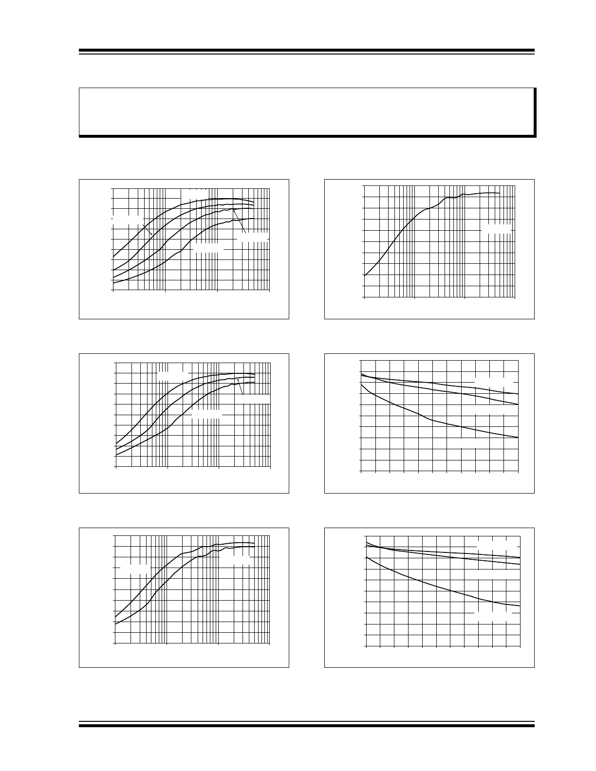
FIGURE 2-1:
3.3V V
OUT
Efficiency vs.
I
OUT
.
FIGURE 2-2:
5V V
OUT
Efficiency vs. I
OUT
.
FIGURE 2-3:
12V V
OUT
Efficiency vs. I
OUT
.
FIGURE 2-4:
24V V
OUT
Efficiency vs.
I
OUT
.
FIGURE 2-5:
3.3V V
OUT
Efficiency vs.
V
IN
.
FIGURE 2-6:
5V V
OUT
Efficiency vs. V
IN
.
Note:
The graphs and tables provided following this note are a statistical summary based on a limited number of
samples and are provided for informational purposes only. The performance characteristics listed herein
are not tested or guaranteed. In some graphs or tables, the data presented may be outside the specified
operating range (e.g., outside specified power supply range) and therefore outside the warranted range.
0
10
20
30
40
50
60
70
80
90
100
1
10
100
1000
Efficiency
(%
)
I
OUT
(mA)
V
IN
= 6V
V
IN
= 12V
V
IN
= 24V
V
IN
= 48V
0
10
20
30
40
50
60
70
80
90
100
1
10
100
1000
Efficiency
(%
)
I
OUT
(mA)
V
IN
= 12V
V
IN
= 24V
V
IN
= 48V
0
10
20
30
40
50
60
70
80
90
100
1
10
100
1000
Efficiency
(%
)
I
OUT
(mA)
V
IN
= 24V
V
IN
= 48V
0
10
20
30
40
50
60
70
80
90
100
1
10
100
1000
Efficiency
(%
)
I
OUT
(mA)
V
IN
= 48V
0
10
20
30
40
50
60
70
80
90
100
6
10
14
18
22
26
30
34
38
42
46
50
Efficiency
(%
)
V
IN
(V)
I
OUT
= 10 mA
I
OUT
= 100 mA
I
OUT
= 500 mA
0
10
20
30
40
50
60
70
80
90
100
6
10
14
18
22
26
30
34
38
42
46
50
Efficiency
(%
)
V
IN
(V)
I
OUT
= 10 mA
I
OUT
= 100 mA
I
OUT
= 500 mA
MCP16331
DS20005308C-page 6
2014-2016 Microchip Technology Inc.
Note:
Unless otherwise indicated, V
IN
= EN = 12V, C
OUT
= C
IN
= 2 x10 µF, L
= 15 µH, V
OUT
= 3.3V, I
LOAD
= 100 mA,
T
A
= +25°C, 6-Lead SOT-23 package
.
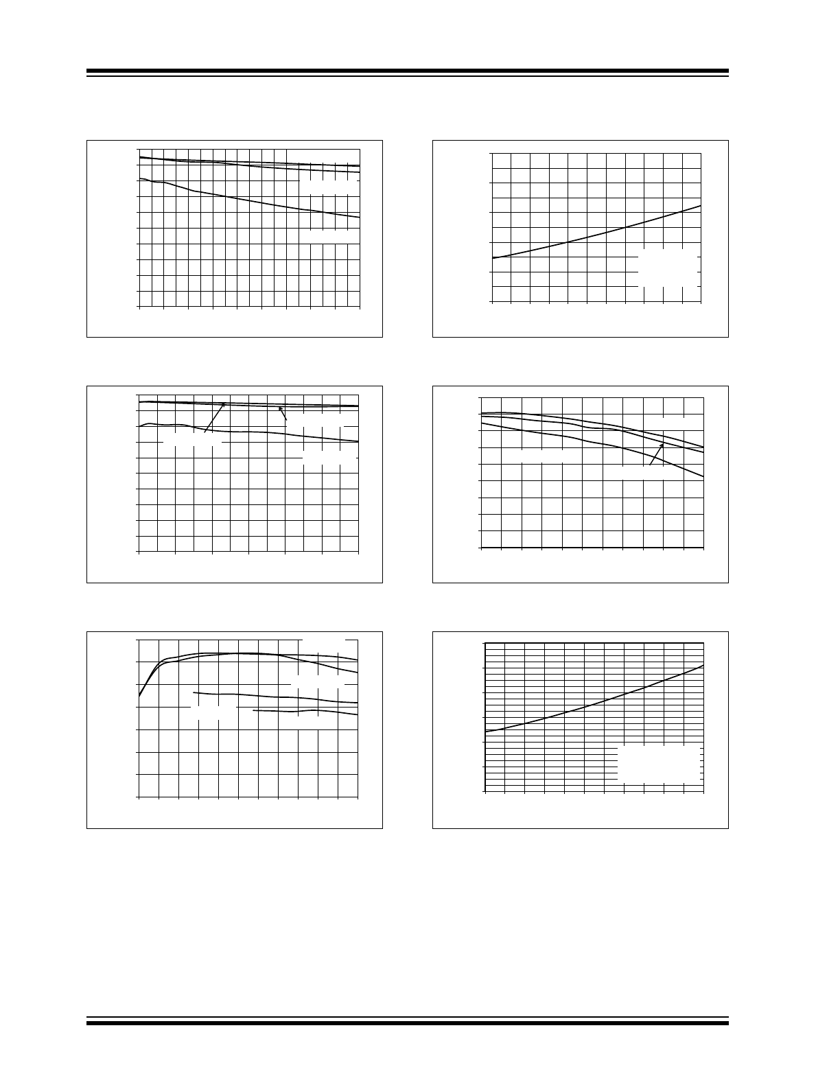
FIGURE 2-7:
12V V
OUT
Efficiency vs. V
IN
.
FIGURE 2-8:
24V V
OUT
Efficiency vs. V
IN
.
FIGURE 2-9:
Max I
OUT
vs. V
IN
.
FIGURE 2-10:
V
FB
vs. Temperature.
FIGURE 2-11:
Peak Current Limit vs.
Temperature.
FIGURE 2-12:
Switch R
DSON
vs.
Temperature.
0
10
20
30
40
50
60
70
80
90
100
14
18
22
26
30
34
38
42
46
50
Efficiency
(%
)
V
IN
(V)
I
OUT
= 10 mA
I
OUT
= 100 mA
I
OUT
= 500 mA
0
10
20
30
40
50
60
70
80
90
100
26
30
34
38
42
46
50
Efficiency
(%
)
V
IN
(V)
I
OUT
= 10 mA
I
OUT
= 100 mA
I
OUT
= 500 mA
0
200
400
600
800
1000
1200
1400
6
10
14
18
22
26
30
34
38
42
46
50
I
OUT
(mA)
V
IN
(V)
V
OUT
= 3.3V
V
OUT
= 5V
V
OUT
= 12V
V
OUT
= 24V
0.78
0.79
0.8
0.81
0.82
0.83
-40 -25 -10
5
20 35 50 65 80 95 110 125
Feedback V
o
ltage (V)
Temperature (°C)
V
IN
=12V
V
OUT
= 3.3V
I
OUT
= 100 mA
0
0.2
0.4
0.6
0.8
1
1.2
1.4
1.6
1.8
-40 -25 -10
5
20
35
50
65
80
95 110 125
Peak Current Limit
(A)
Temperature (°C)
V
OUT
= 3.3V
V
OUT
= 5V
V
OUT
= 12V
0
0.2
0.4
0.6
0.8
1
1.2
-40 -25 -10
5
20
35
50
65
80
95 110 125
Sw
itch R
DSON
(Ω
)
Temperature (°C)
V
IN
= 6V
V
OUT
=V
BOOST
= 3.3V
I
OUT
= 200 mA
2014-2016 Microchip Technology Inc.
DS20005308C-page 7
MCP16331
Note:
Unless otherwise indicated, V
IN
= EN = 12V, C
OUT
= C
IN
= 2 x10 µF, L
= 15 µH, V
OUT
= 3.3V, I
LOAD
= 100 mA,
T
A
= +25°C, 6-Lead SOT-23 package
.
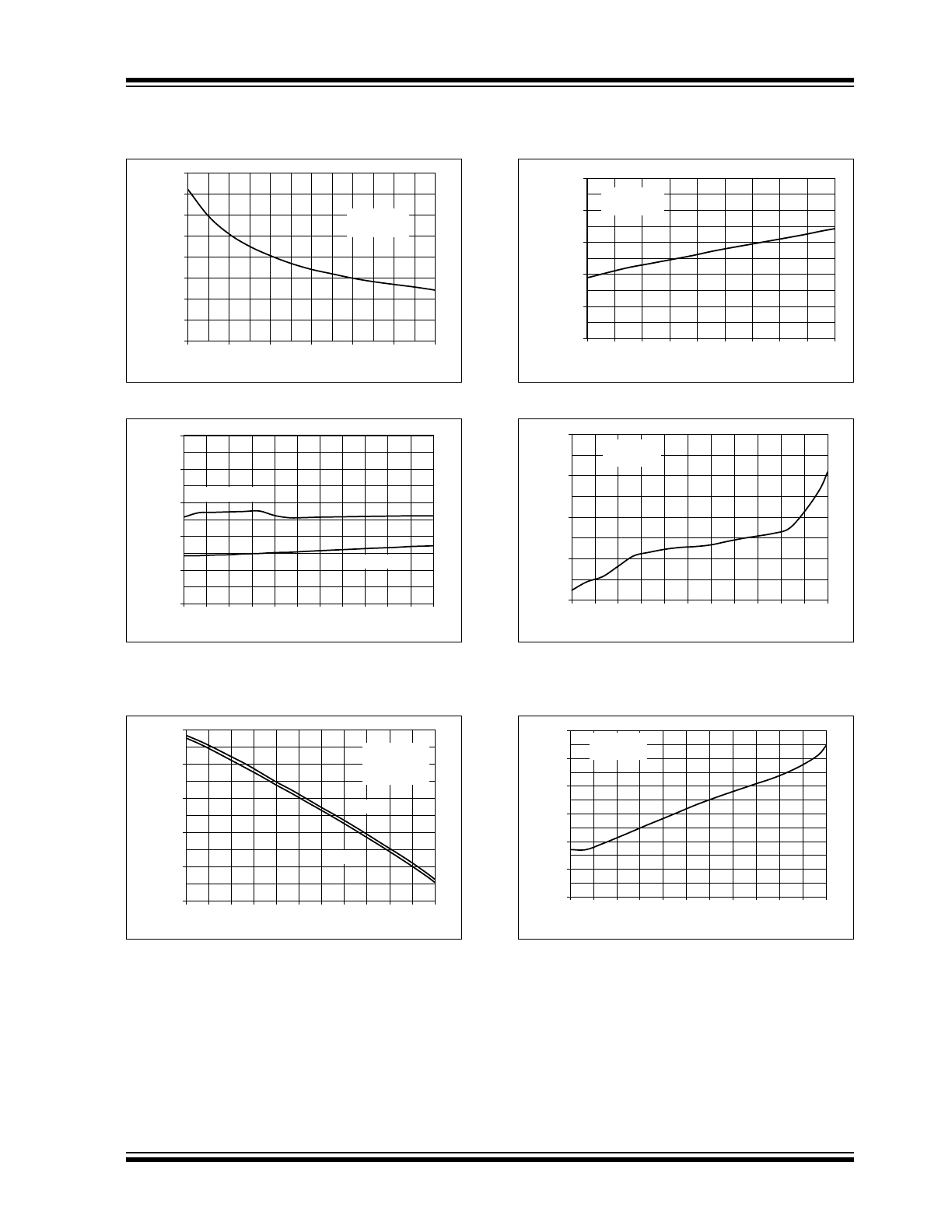
FIGURE 2-13:
Switch R
DSON
vs. V
BOOST
.
FIGURE 2-14:
Undervoltage Lockout vs.
Temperature.
FIGURE 2-15:
EN Threshold Voltage vs.
Temperature.
FIGURE 2-16:
V
OUT
vs. V
IN
.
FIGURE 2-17:
Input Quiescent Current vs.
Temperature.
FIGURE 2-18:
Shutdown Current vs.
Temperature.
0.4
0.45
0.5
0.55
0.6
0.65
0.7
0.75
0.8
2.5
3
3.5
4
4.5
5
5.5
Sw
itch R
DSON
(Ω
)
V
BOOST
(V)
V
IN
= 6V
V
OUT
= 3.3V
3
3.4
3.8
4.2
4.6
5
-40 -25 -10
5
20
35
50
65
80
95 110 125
Input V
o
ltage (V)
Temperature (°C)
UVLO START
UVLO STOP
0.9
1
1.1
1.2
1.3
1.4
-40 -25 -10
5
20
35
50
65
80
95 110 125
Enable V
o
ltage (V)
Temperature (°C)
UP
DOWN
V
IN
= 12V
V
OUT
= 3.3V
I
OUT
= 100 mA
3.27
3.275
3.28
3.285
3.29
3.295
5
10
15
20
25
30
35
40
45
50
V
OUT
(V)
V
IN
(V)
V
OUT
= 3.3V
I
OUT
=100 mA
0.8
0.9
1
1.1
1.2
-40 -25 -10
5
20
35
50
65
80
95 110 125
No Load Input Current (mA)
Temperature (°C)
V
IN
= 12V
V
OUT
= 3.3V
4
4.5
5
5.5
6
6.5
7
-40 -25 -10
5
20
35
50
65
80
95 110 125
Shutdow
n Current
(µA)
Temperature (°C)
V
IN
= 12V
V
OUT
= 3.3V
MCP16331
DS20005308C-page 8
2014-2016 Microchip Technology Inc.
Note:
Unless otherwise indicated, V
IN
= EN = 12V, C
OUT
= C
IN
= 2 x10 µF, L
= 15 µH, V
OUT
= 3.3V, I
LOAD
= 100 mA,
T
A
= +25°C, 6-Lead SOT-23 package
.
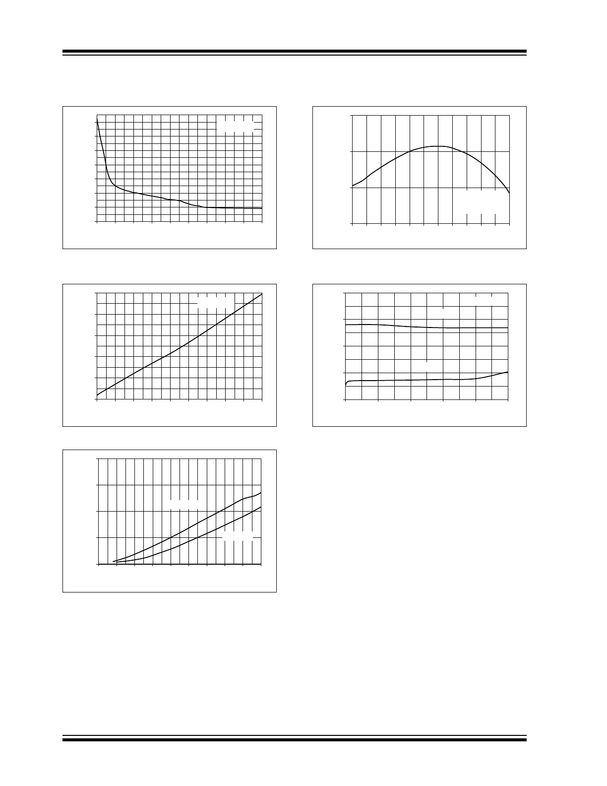
FIGURE 2-19:
Input Quiescent Current vs.
V
IN
.
FIGURE 2-20:
Shutdown Current vs. V
IN
.
FIGURE 2-21:
PWM/Skipping I
OUT
Threshold vs. V
IN
.
FIGURE 2-22:
Switching Frequency vs.
Temperature.
FIGURE 2-23:
Minimum Input Voltage vs.
Output Current.
0.5
0.7
0.9
1.1
1.3
1.5
1.7
1.9
5
10
15
20
25
30
35
40
45
50
No Load Input Current (mA)
V
IN
(V)
V
OUT
= 3.3V
3
6
9
12
15
18
5
10
15
20
25
30
35
40
45
50
Shutdow
n Current
(µA)
V
IN
(V)
V
OUT
= 3.3V
0
5
10
15
20
5
10
15
20
25
30
35
40
45
50
Output Current (mA)
V
IN
(V)
V
OUT
= 5V
V
OUT
= 3.3V
450
475
500
525
-40 -25 -10
5
20
35
50
65
80
95 110 125
Sw
itching Frequency
(kHz)
Temperature (°C)
V
IN
= 12V
V
OUT
= 3.3V
I
OUT
= 200 mA
3.5
3.7
3.9
4.1
4.3
0
0.1
0.2
0.3
0.4
0.5
V
IN
(V)
Output Current (A)
To Start
To Stop
V
OUT
=3.3V
2014-2016 Microchip Technology Inc.
DS20005308C-page 9
MCP16331
Note:
Unless otherwise indicated, V
IN
= EN = 12V, C
OUT
= C
IN
= 2 x10 µF, L
= 15 µH, V
OUT
= 3.3V, I
LOAD
= 100 mA,
T
A
= +25°C, 6-Lead SOT-23 package
.
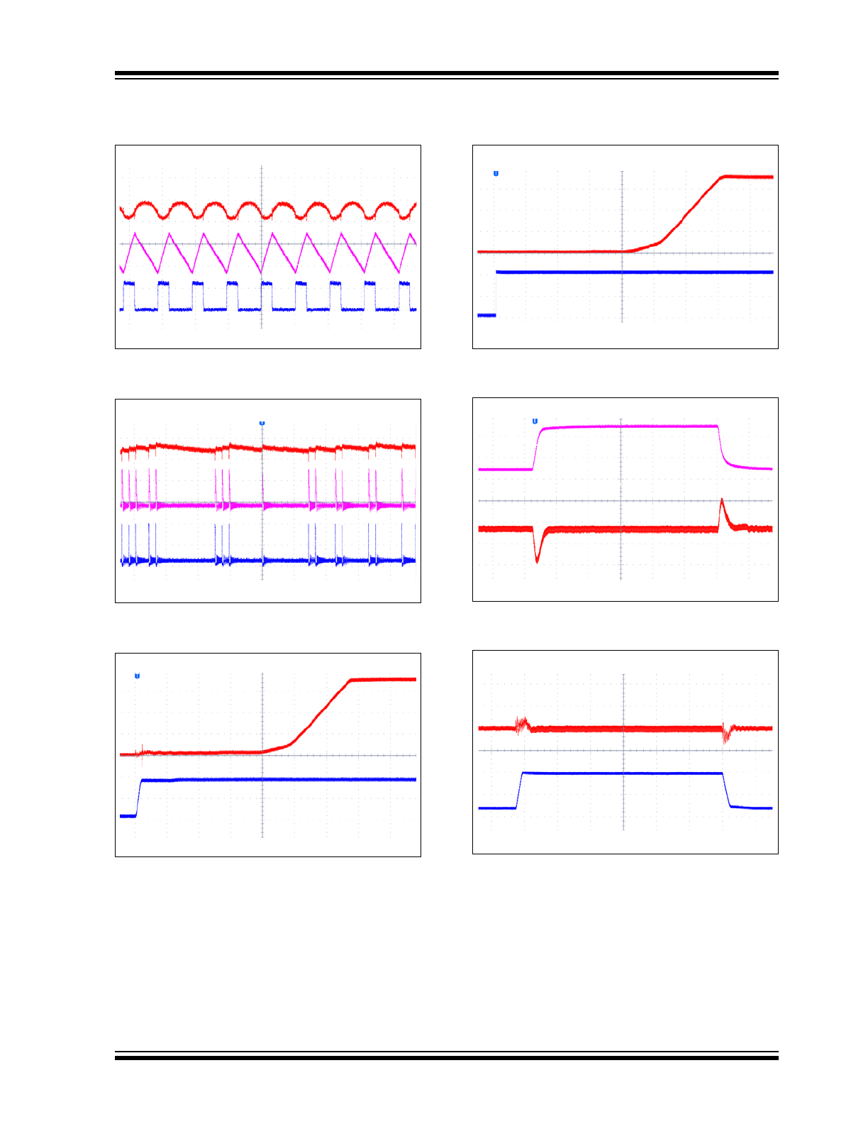
FIGURE 2-24:
Heavy Load Switching
Waveforms.
FIGURE 2-25:
Light Load Switching
Waveforms.
FIGURE 2-26:
Start-up from V
IN
.
FIGURE 2-27:
Start-up from EN.
FIGURE 2-28:
Load Transient Response.
FIGURE 2-29:
Line Transient Response.
V
IN
= 12V
V
OUT
= 3.3V
I
OUT
= 300 mA
2 µs/div
V
OUT
20 mV/div
AC coupled
IL
200 mA/div
SW
10V/div
V
IN
= 48V
V
OUT
= 3.3V
I
OUT
= 5 mA
V
OUT
20 mV/div
AC coupled
IL
50 mA/div
SW
20V/div
10 µs/div
V
IN
= 36V
V
OUT
= 3.3V
I
OUT
= 200 mA
V
OUT
1V/div
V
IN
20V/div
80 µs/div
V
OUT
1V/div
V
IN
= 12V
V
OUT
= 3.3V
I
OUT
= 200 mA
80 µs/div
EN
2V/div
V
IN
= 12V
V
OUT
= 3.3V
Load Step from
100 mA to 500 mA
V
OUT
50 mV/div
AC coupled
200 µs/div
I
OUT
200 mA/div
V
OUT
= 3.3V
I
OUT
= 200 mA
Line Step from
5V to 24V
200 µs/div
V
OUT
100 mV/div
AC coupled
V
IN
10V/div
MCP16331
DS20005308C-page 10
2014-2016 Microchip Technology Inc.
3.0
PIN DESCRIPTIONS
The descriptions of the pins are listed in
Table 3-1
.
3.1
Switch Node (SW)
The switch node pin is connected internally to the
NMOS switch, and externally to the SW node consist-
ing of the inductor and Schottky diode. The external
Schottky diode should be connected close to the SW
node and GND.
3.2
Enable Pin (EN)
The EN pin is a logic-level input used to enable or
disable the device switching and lower the quiescent
current while disabled. By default the MCP16331 is
enabled through an internal pull-up. To turn off the
device, the EN pin must be pulled low.
3.3
Ground Pin (GND)
The ground or return pin is used for circuit ground con-
nection. The length of the trace from the input cap return,
output cap return and GND pin should be made as short
as possible to minimize the noise on the GND pin.
3.4
Feedback Voltage Pin (V
FB
)
The V
FB
pin is used to provide output voltage regulation
by using a resistor divider. The V
FB
voltage will be 0.8V
typical with the output voltage in regulation.
3.5
Boost Pin (BOOST)
The supply for the floating high-side driver, used to turn
the integrated N-Channel MOSFET on and off, is
connected to the BOOST pin.
3.6
Power Supply Input Voltage Pin
(V
IN
)
Connect the input voltage source to V
IN
. The input
source should be decoupled to GND with a 4.7 µF-20 µF
capacitor, depending on the impedance of the source
and output current. The input capacitor provides current
for the switch node and a stable voltage source for the
internal device power. This capacitor should be
connected as close as possible to the V
IN
and GND pins.
3.7
Exposed Thermal Pad Pin (EP)
There is an internal electrical connection between the
EP and GND pin for the TDFN package.
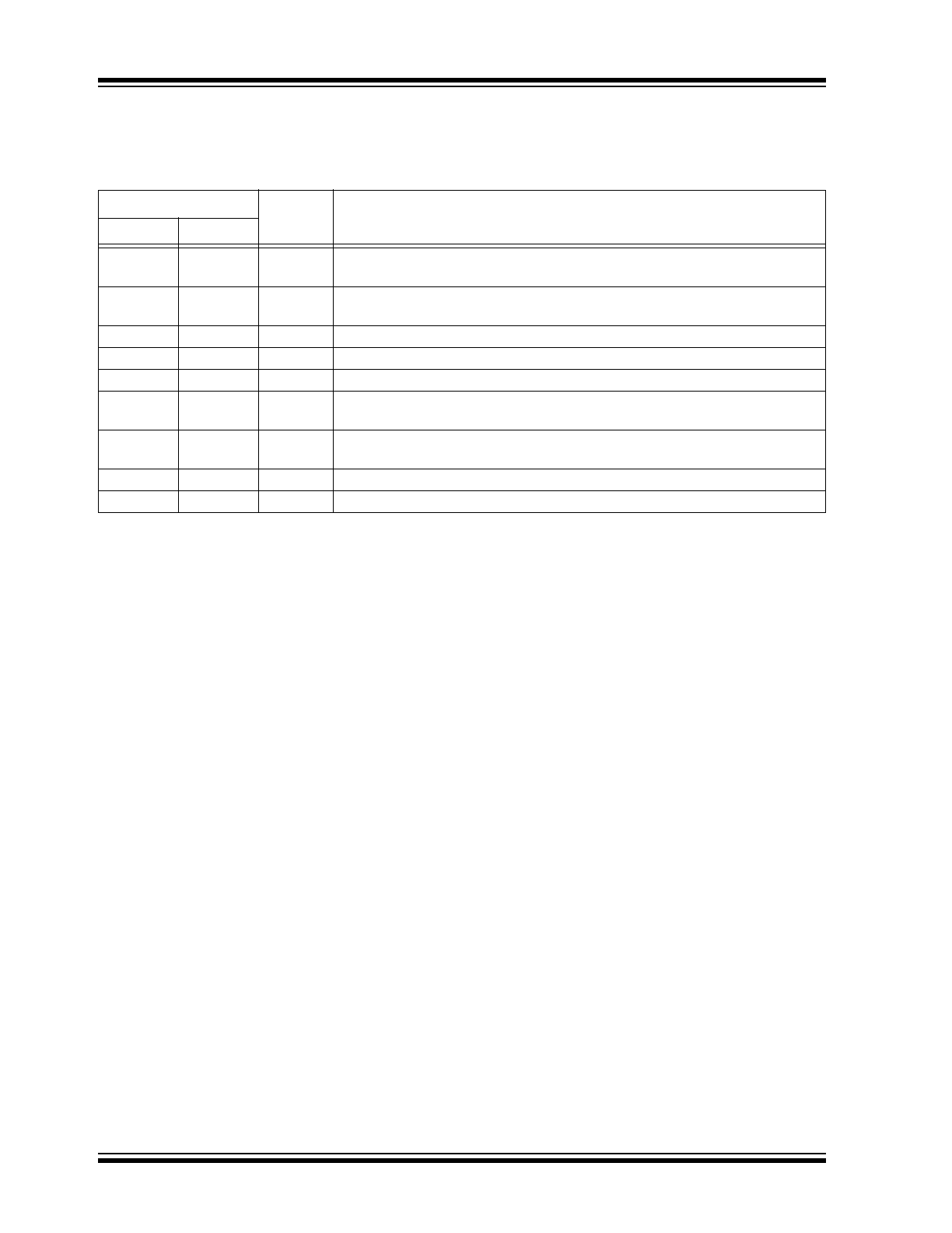
TABLE 3-1:
PIN FUNCTION TABLE
MCP16331
Symbol
Description
TDFN
SOT-23
1
6
SW
Output switch node. Connects to the inductor, freewheeling diode and the
bootstrap capacitor.
2
4
EN
Enable pin. There is an internal pull-up on the V
IN
. To turn the device off,
connect EN to GND.
3
—
NC
Not connected.
4
—
NC
Not connected.
5
2
GND
Ground pin.
6
3
V
FB
Output voltage feedback pin. Connect V
FB
to an external resistor divider to set
the output voltage.
7
1
BOOST
Boost voltage that drives the internal NMOS control switch. A bootstrap
capacitor is connected between the BOOST and SW pins.
8
5
V
IN
Input supply voltage pin for power and internal biasing.
9
—
EP
Exposed Thermal Pad