
2013 Microchip Technology Inc.
DS20005254A-page 1
MCP1632
Features:
• High-Speed PWM Controller with Integrated
Low-Side MOSFET Driver
• Multiple Switching Frequency Options (f
SW
):
- 300 kHz
- 600 kHz
• Adjustable Reference Voltage Generator
• Adjustable Soft Start
• Internal Slope Compensation
• Shutdown Input Pin (EN)
• Low Operating Current: < 5 mA (typical)
• Undervoltage Lockout (UVLO) Protection
• Output Short Circuit Protection
• Overtemperature Protection
• Operating Temperature Range:
- -40°C to +125°C
Applications:
• Switch Mode Power Supplies
• Brick DC-DC Converters
• Battery Charger Applications
• LED Drivers
Related Literature:
• “MCP1632 300 kHz Boost Converter Demo Board
User’s Guide”, Microchip Technology Inc.,
DS20005252A, 2013
Description:
The MCP1632 high-speed PWM controller is a
pulse-width modulator developed for stand-alone power
supply applications. The MCP1632 includes a
high-speed analog control loop, a logic-level MOSFET
driver, an internal oscillator, a reference voltage
generator, and internal slope compensation. This high
level of integration makes it an ideal solution for
standalone SMPS applications. MCP1632 is suitable for
use in topologies requiring a low-side MOSFET control,
such as Boost, Flyback, SEPIC, Ćuk, etc. Typical
applications include battery chargers, intelligent power
systems, brick DC-DC converters, LED drivers. Due to
its low power consumption, the MCP1632 PWM
controller is recommended for battery-operated
applications.
The MCP1632 offers a Peak Current mode control in
order to achieve consistent performance regardless of
the topology of the power train or the operating
conditions. In addition, the MCP1632 can implement
the Voltage Mode Control for cost-sensitive solutions.
The MCP1632 PWM controller can be easily interfaced
with PIC microcontrollers in order to develop an
intelligent power solution.
Additional features include: UVLO, overtemperature
and overcurrent protection, shutdown capability (EN
pin) and an adjustable soft start option.
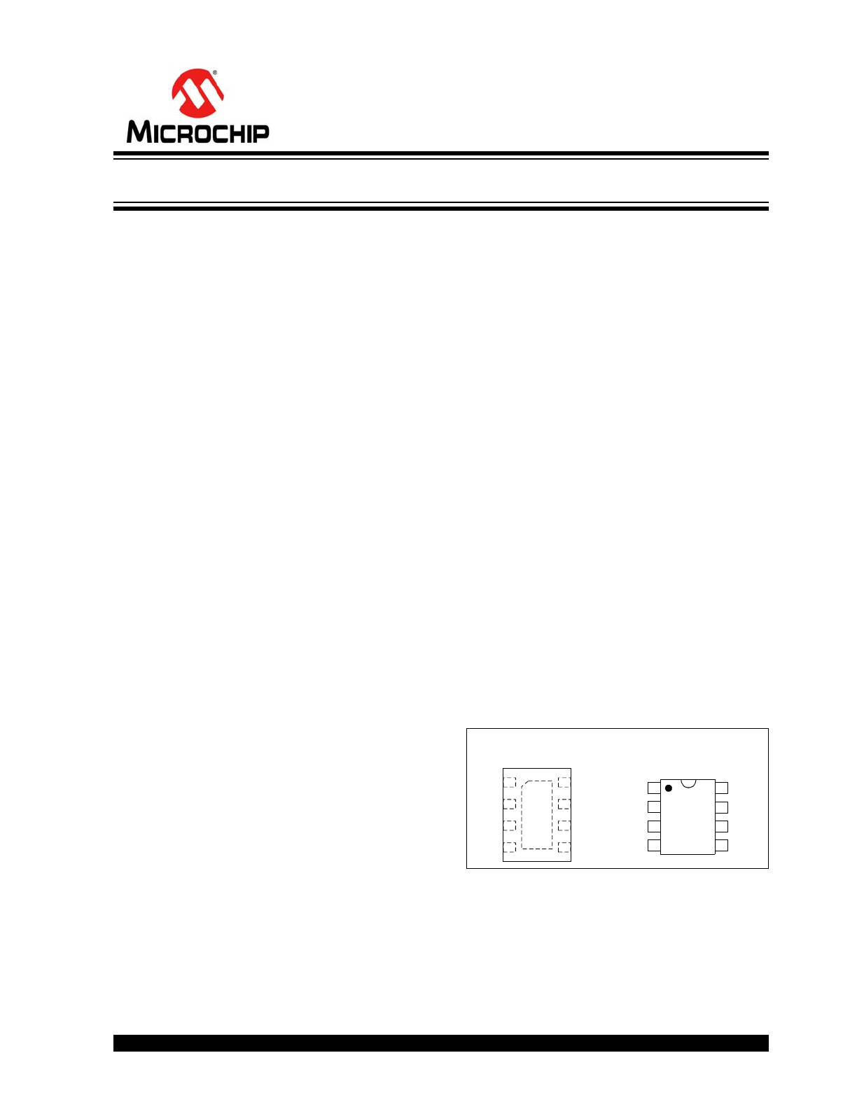
Package Type
1
2
3
4
8
7
6
5
COMP
FB
CS
EN
GND
V
EXT
Vin
V
REF
EP
9
8-Lead DFN
1
2
3
4
8
7
6
5
FB
CS
EN
COMP
V
IN
V
REF
V
EXT
GND
8-Lead MSOP
(2 mm x 3 mm)
High-Speed, Low-Side PWM Controller
MCP1632
DS20005254A-page 2
2013 Microchip Technology Inc.
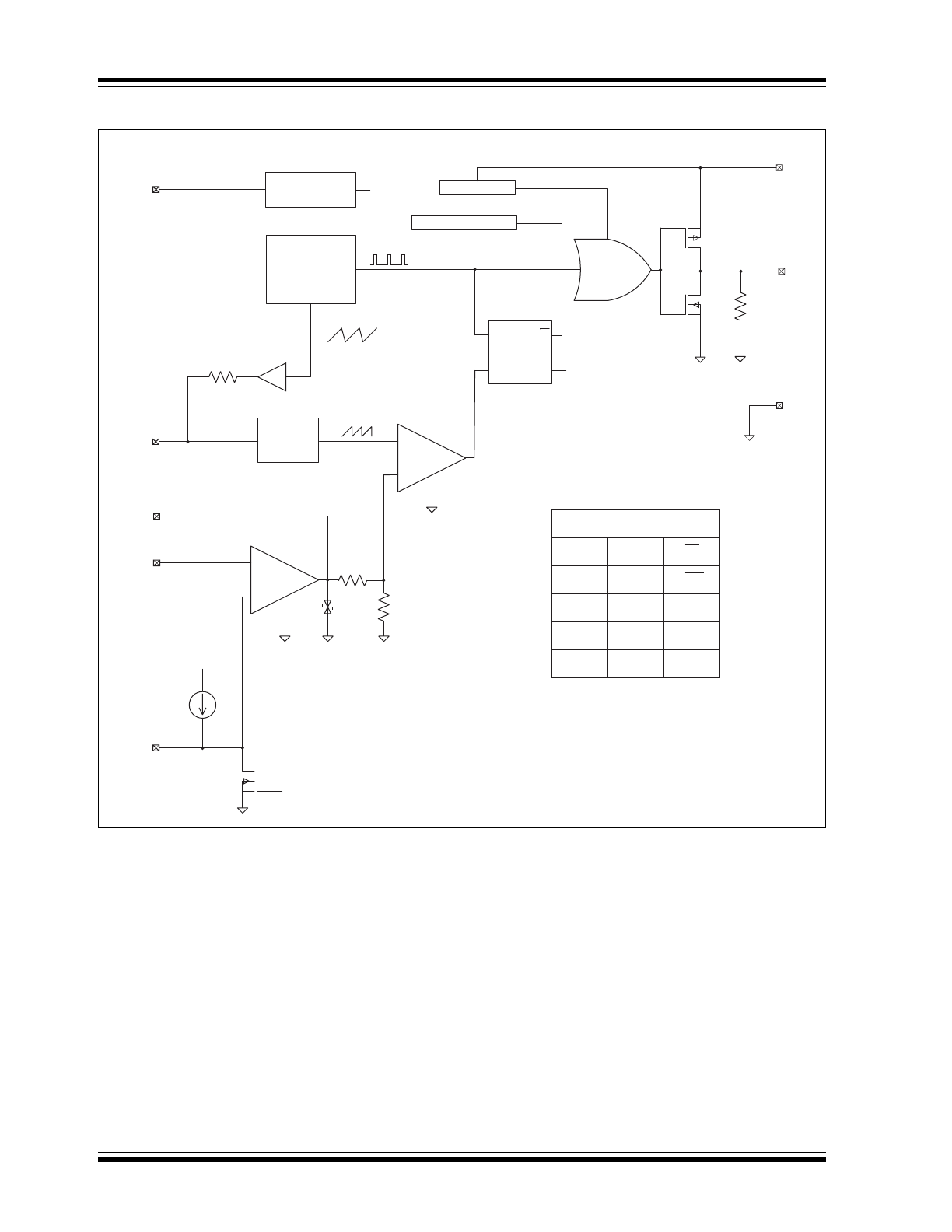
Functional Block Diagram
V
EXT
10 k
:
Oscillator
EN
UVLO
Overtemperature
Q
Q
S
R
GND
PWM
Comp
+
-
CS
V
IN
V
IN
V
IN
EA
V
IN
2R
R
2.7V
COMP
FB
V
REF
Latch Truth Table
S
R
Q
0
1
0
0
1
1
1
1
1
0
0
Qn
+
-
300/600 kHz
V
IN
50 μA
CLK
Reference
Voltage
V
DRIVE
RAMP
+1
6 k
:
Shutdown
Circuit
SS Reset
SS Reset
CS
Blanking
100 ns
2013 Microchip Technology Inc.
DS20005254A-page 3
MCP1632
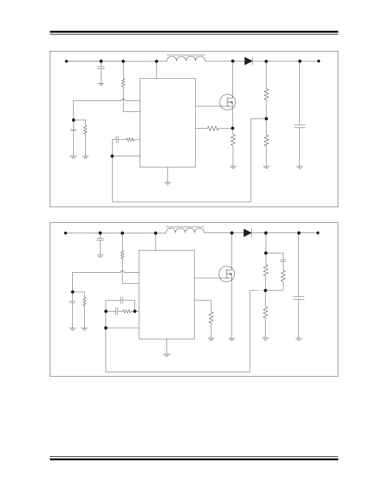
Typical Application Circuit – Peak Current Mode Control
Typical Application Circuit – Voltage Mode Control
MCP1632
R
R
C
SS
V
IN
V
OUT
V
REF
COMP
EN
FB
CS
V
EXT
GND
V
CC
MCP1632
R
R
C
SS
V
IN
V
OUT
V
REF
COMP
EN
FB
CS
V
EXT
GND
V
CC
MCP1632
DS20005254A-page 4
2013 Microchip Technology Inc.
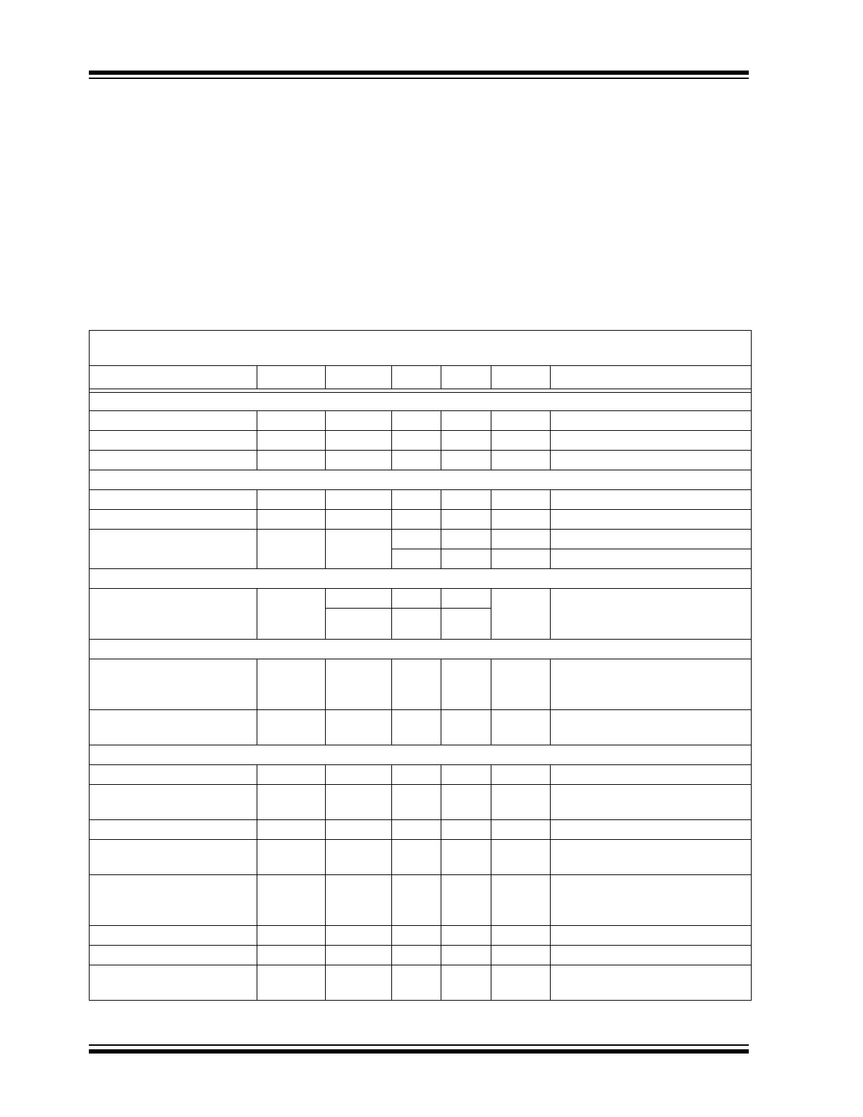
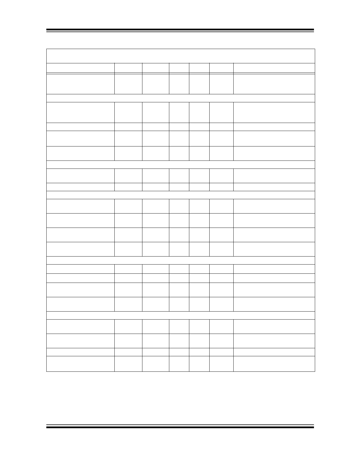
1.0
ELECTRICAL
CHARACTERISTICS
Absolute Maximum Ratings †
V
DD
...................................................................................6.0V
Maximum Voltage on Any Pin . (V
GND
– 0.3)V to (V
IN
+ 0.3)V
V
EXT
Short Circuit Current ...........................Internally Limited
Storage Temperature.....................................-65°C to +150°C
Maximum Junction Temperature, T
J
........................... +150°C
Continuous Operating Temperature Range ..-40°C to +125°C
ESD protection on all pins, HBM
2 kV
† Notice:
Stresses above those listed under “Maximum
Ratings” may cause permanent damage to the device.
This is a stress rating only and functional operation of
the device at those or any other conditions above those
indicated in the operational listings of this specification
is not implied. Exposure to maximum rating conditions
for extended periods may affect device reliability.
AC/DC CHARACTERISTICS
Electrical Specifications:
Unless otherwise noted, V
IN
= 3.0V to 5.5V, F
OSC
= 300 kHz, C
IN
= 0.1 µF,
V
IN
for typical values = 5.0V, T
A
= -40°C to +125°C.
Parameters
Sym.
Min.
Typ.
Max.
Units
Conditions
Input Voltage
Input Operating Voltage
V
IN
3.0
—
5.5
V
Input Quiescent Current
I(V
IN
)
—
5
7.5
mA
I
EXT
= 0 mA
Input Shutdown Current
I(V
IN
)
SHDN
—
—
2
µA
EN = 0V
EN Input
EN Input Voltage Low
EN
LOW
—
—
0.8
V
EN Input Voltage High
EN
HIGH
75
—
—
% of V
IN
Delay Time
—
—
190
210
µs
EN goes from low to high (
Note 1
)
40
60
µs
EN goes from high to low (
Note 1
)
Internal Oscillator
Internal Oscillator Range
F
OSC
250
300
350
kHz
Two options
Refer to
Section 4.8 “Internal
Oscillator”
.
510
600
690
Reference Voltage Section
Reference Voltage
Input Range
V
REF
0
—
V
IN
V
Note 1
Refer to
Section 4.7 “Reference
Voltage Generator”
for details.
Internal Constant Current
Generator
I
REF
48
50
52
µA
Refer to
Section 4.7 “Reference
Voltage Generator”
for details.
Error Amplifier
Input Offset Voltage
V
OS
-4
0.1
+4
mV
Error Amplifier
PSRR
65
80
—
dB
V
IN
= 3.0V to 5.0V, V
CM
= 1.2V
(
Note 1
)
Common-Mode Input Range
V
CM
GND - 0.3
—
V
IN
V
Note 1
Common-Mode
Rejection Ratio
CMRR
60
80
—
dB
V
IN
= 5V, V
CM
= 0V to 2.5V
(
Note 1
)
Open-Loop Voltage Gain
A
VOL
80
95
—
dB
R
L
= 5 k
to V
IN
/2,
100 mV < V
EAOUT
< V
IN
- 100 mV,
V
CM
= 1.2V (
Note 1
)
Low-Level Output
V
OL
—
25
50
mV
R
L
= 5 k
to V
IN
/2
Gain Bandwidth Product
GBWP
3.5
5
—
MHz
V
IN
= 5V (
Note 1
)
Error Amplifier Sink Current
I
SINK
4
8
—
mA
V
IN
= 5V, V
REF
= 1.2V,
V
FB
= 1.4V, V
COMP
= 2.0V
Note 1:
Ensured by design. Not production tested.
2013 Microchip Technology Inc.
DS20005254A-page 5
MCP1632
Error Amplifier
Source Current
I
SOURCE
4
6
—
mA
V
IN
= 5V, V
REF
= 1.2V,
V
FB
= 1.0V, V
COMP
= 2.0V,
Absolute Value
Current Sense Input
Maximum Current Sense
Signal
V
CS_MAX
0.8
0.9
0.97
V
Set by maximum error amplifier
clamp voltage, divided by 3
(
Note 1
)
Blanking Time
T
BLANK
80
100
130
ns
Note 1
Delay from CS to V
EXT
T
CS_VEXT
—
—
35
ns
Excluding the blanking time
(
Note 1
)
Current Sense Input Bias
Current
I
CS_B
—
-0.1
—
µA
Note 1
PWM Section
Minimum Duty Cycle
DC
MIN
—
—
0
%
V
FB
= V
REF
+ 0.1V, V
CS
= GND
(
Note 1
)
Maximum Duty Cycle
DC
MAX
80
85
95
%
Slope Compensation Ramp Generator
Ramp Amplitude
V
RAMP
0.8
0.9
1
V
PP
Refer to
Section 4.6 “Slope
Compensation”
for details.
DC Offset Low
—
0.15
0.32
0.45
V
Refer to
Section 4.6 “Slope
Compensation”
for details.
DC Offset High
—
1.12
1.22
1.32
V
Refer to
Section 4.6 “Slope
Compensation”
for details.
Ramp Generator Output
Impedance
Z
RG
5.5
6
6.5
k
Refer to
Section 4.6 “Slope
Compensation”
for details.
Internal Driver
R
DSon
P-channel
R
DSon_P
—
10
30
R
DSon
N-channel
R
DSon_N
—
7
30
V
EXT
Rise Time
T
RISE
—
—
18
ns
C
L
= 100 pF
Typical for V
IN
= 3V (
Note 1
)
V
EXT
Fall Time
T
FALL
—
—
18
ns
C
L
= 100 pF
Typical for V
IN
= 3V (
Note 1
)
Protection Features
Undervoltage Lockout
UVLO
2.6
—
2.9
V
V
IN
falling,
V
EXT
low state when in UVLO
Undervoltage Lockout
Hysteresis
UVLO
HYS
50
110
180
mV
Thermal Shutdown
T
SHD
—
150
—
°C
Note 1
Thermal Shutdown
Hysteresis
T
SHD_HYS
—
20
—
°C
Note 1
AC/DC CHARACTERISTICS (CONTINUED)
Electrical Specifications:
Unless otherwise noted, V
IN
= 3.0V to 5.5V, F
OSC
= 300 kHz, C
IN
= 0.1 µF,
V
IN
for typical values = 5.0V, T
A
= -40°C to +125°C.
Parameters
Sym.
Min.
Typ.
Max.
Units
Conditions
Note 1:
Ensured by design. Not production tested.
MCP1632
DS20005254A-page 6
2013 Microchip Technology Inc.
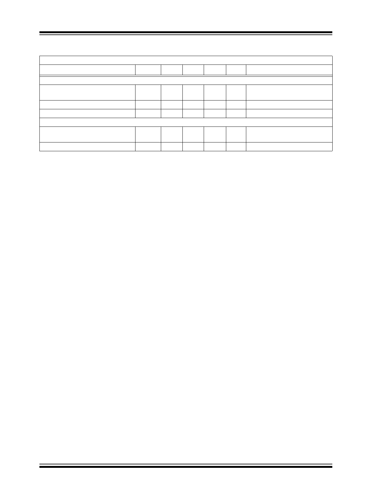
TEMPERATURE SPECIFICATIONS
Electrical Specifications:
V
IN
= 3.0V to 5.5V, F
OSC
= 600 kHz, C
IN
= 0.1 µF. T
A
= -40°C to +125°C.
Parameters
Sym.
Min.
Typ.
Max.
Units
Conditions
Temperature Ranges
Operating Junction Temperature
Range
T
A
-40
—
+125
°C
Steady state
Storage Temperature Range
T
A
-65
—
+150
°C
Maximum Junction Temperature
T
J
—
—
+150
°C
Transient
Thermal Package Resistances
Thermal Resistance,
8L-DFN (2 mm x 3 mm)
JA
—
75
—
°C/W Typical 4-layer board with two
interconnecting vias.
Thermal Resistance, 8L-MSOP
JA
—
211
—
°C/W Typical 4-layer board.
2013 Microchip Technology Inc.
DS20005254A-page 7
MCP1632
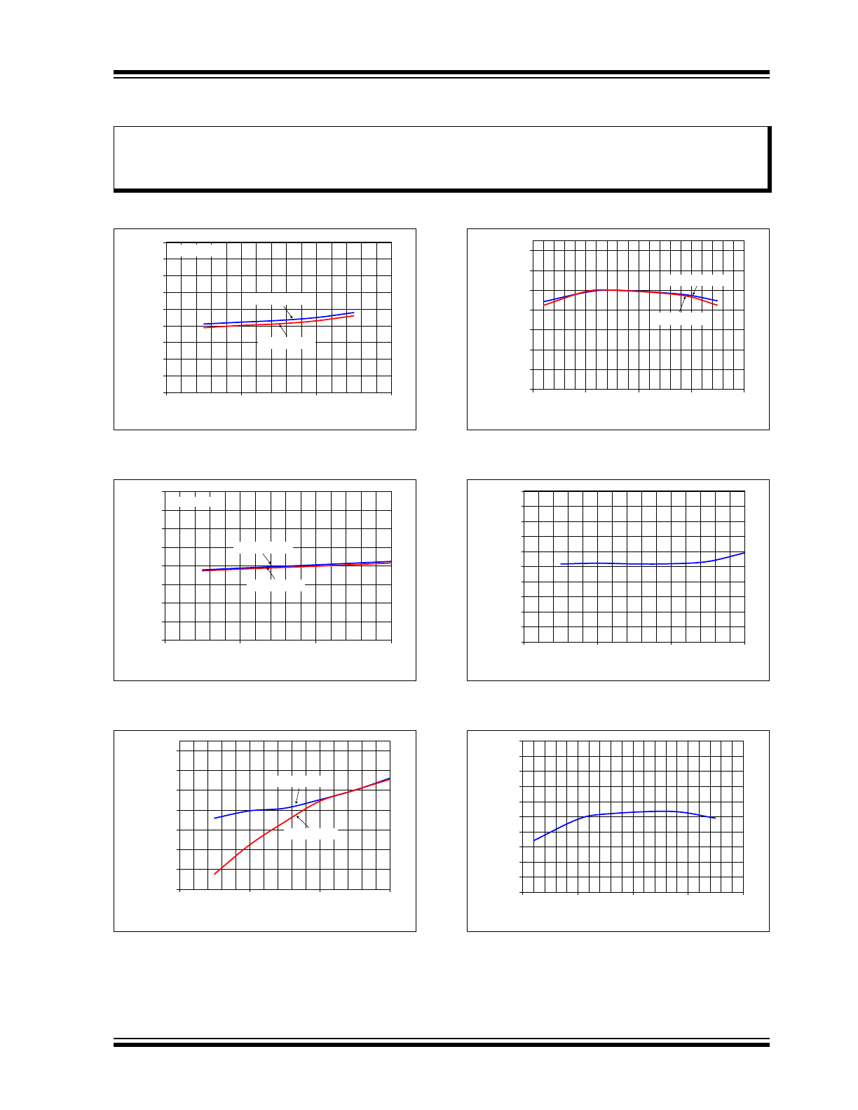
2.0
TYPICAL PERFORMANCE CURVES
Note:
Unless otherwise noted, V
IN
= 5V, F
OSC
= 300 kHz, C
IN
= 0.1 µF, T
A
= 25°C.
FIGURE 2-1:
Input Quiescent Current vs.
Input Voltage (EN = Low).
FIGURE 2-2:
Input Quiescent Current vs.
Input Voltage (EN = High).
FIGURE 2-3:
Relative Oscillator
Frequency Variation vs. Input Voltage.
FIGURE 2-4:
Relative Oscillator
Frequency Variation vs. Junction Temperature.
FIGURE 2-5:
V
REF
Current vs. Input
Voltage.
FIGURE 2-6:
V
REF
Current vs. Junction
Temperature.
Note:
The graphs and tables provided following this note are a statistical summary based on a limited number of
samples and are provided for informational purposes only. The performance characteristics listed herein
are not tested or guaranteed. In some graphs or tables, the data presented may be outside the specified
operating range (e.g., outside specified power supply range) and therefore outside the warranted range.
0.0
0.1
0.2
0.3
0.4
0.5
0.6
0.7
0.8
0.9
2.5
3.5
4.5
5.5
Input
Quiescent Current (μA)
Input Voltage (V)
f
SW
= 600 kHz
f
SW
= 300 kHz
EN = Low
0.0
1.0
2.0
3.0
4.0
5.0
6.0
7.0
8.0
2.5
3.5
4.5
5.5
Input
Quiescent Current (mA)
Input Voltage (V)
f
SW
= 300 kHz
f
SW
= 600 kHz
EN = High
-10.0
-8.0
-6.0
-4.0
-2.0
0.0
2.0
4.0
2.5
3.5
4.5
5.5
Relative Oscillator Frequency
V
a
riation (%
)
Input Voltage (V)
f
SW
= 300 kHz
f
SW
= 600 kHz
-10.0
-8.0
-6.0
-4.0
-2.0
0.0
2.0
4.0
-50
0
50
100
150
Relative Oscillator Frequency
V
a
riation (%
)
Junction Temperature (°C)
f
SW
= 300 kHz
f
SW
= 600 kHz
49.5
49.6
49.7
49.8
49.9
50
50.1
50.2
50.3
50.4
50.5
2.5
3.5
4.5
5.5
V
REF
Current (μA)
Input Voltage (V)
49
49.2
49.4
49.6
49.8
50
50.2
50.4
50.6
50.8
51
-50
0
50
100
150
V
REF
Current (μA)
Junction Temperature (°C)
MCP1632
DS20005254A-page 8
2013 Microchip Technology Inc.
Note:
Unless otherwise noted, V
IN
= 5V, F
OSC
= 300 kHz, C
IN
= 0.1 µF, T
A
= 25°C.
FIGURE 2-7:
Error Amplifier Offset
Voltage vs. Temperature.
FIGURE 2-8:
Error Amplifier Offset
Voltage vs. Input Voltage.
FIGURE 2-9:
V
EXT
Rise Time vs. Input
Voltage.
FIGURE 2-10:
V
EXT
Fall Time vs. Input
Voltage.
FIGURE 2-11:
Relative V
EXT
N-Channel
MOSFET R
DSon
Variation vs. Input Voltage.
FIGURE 2-12:
Relative V
EXT
P-Channel
MOSFET R
DSon
Variation vs. Input Voltage.
-0.5
-0.4
-0.3
-0.2
-0.1
0
0.1
0.2
-50
0
50
100
150
Error Amplifier
Offset
V
o
ltage
(mV)
Junction Temperature (°C)
NMOS Pair
PMOS Pair
-1
-0.8
-0.6
-0.4
-0.2
0
0.2
0.4
0.6
2.5
3.5
4.5
5.5
Error Amplifier
Offset
V
o
ltage
(mV)
Input Voltage (V)
NMOS Pair
PMOS Pair
2
3
4
5
2.5
3.5
4.5
5.5
V
EXT
Rise T
ime (ns)
Input Voltage (V)
C
LOAD
= 100 pF
2
3
4
5
2.5
3.5
4.5
5.5
V
EXT
Fall T
ime (ns)
Input Voltage (V)
C
LOAD
= 100 pF
-5.0
0.0
5.0
10.0
15.0
20.0
25.0
30.0
35.0
40.0
45.0
2.5
3.5
4.5
5.5
Relative V
EXT
N-Channel
MOSFET R
DSon
V
a
riation (%
)
Input Voltage (V)
-10.0
-5.0
0.0
5.0
10.0
15.0
20.0
25.0
30.0
35.0
40.0
45.0
2.5
3.5
4.5
5.5
Relative V
EXT
P-Channel
MOSFET R
DSon
V
a
riation (%
)
Input Voltage (V)
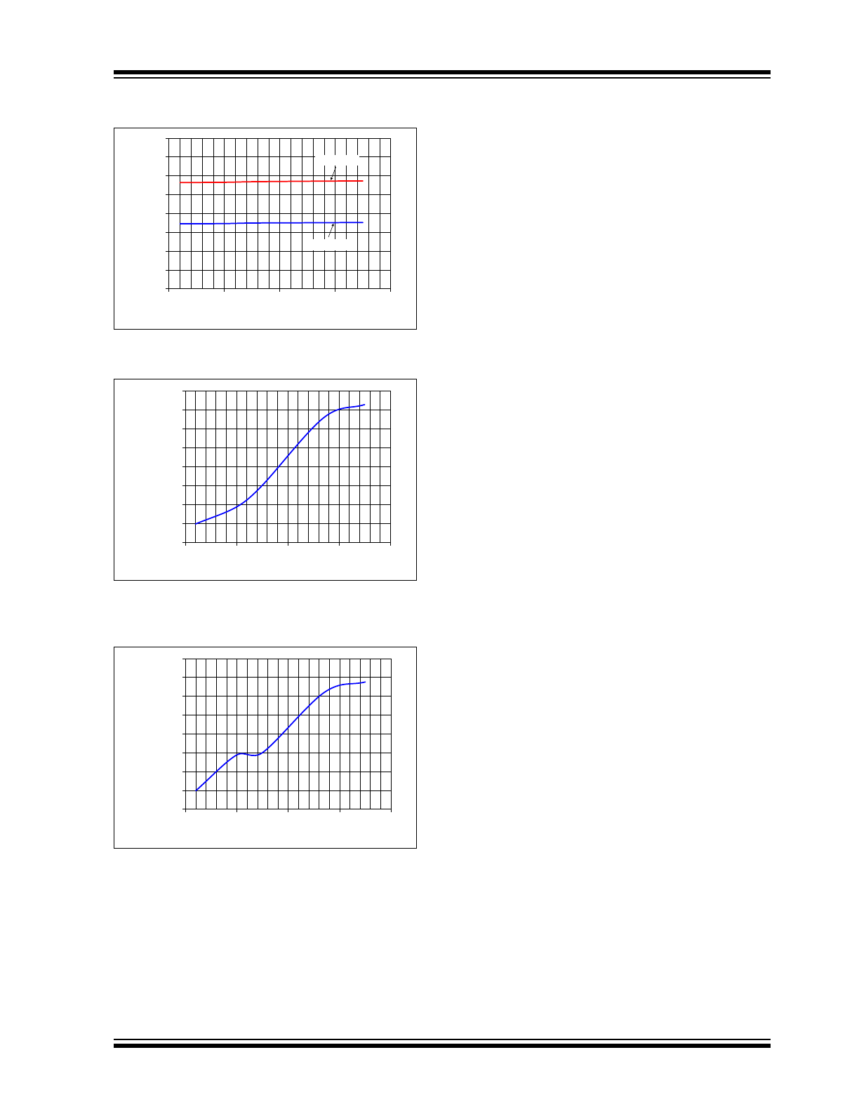
2013 Microchip Technology Inc.
DS20005254A-page 9
MCP1632
Note:
Unless otherwise noted, V
IN
= 5V, F
OSC
= 300 kHz, C
IN
= 0.1 µF, T
A
= 25°C.
FIGURE 2-13:
UVLO Threshold vs.
Temperature.
FIGURE 2-14:
Relative V
EXT
N-Channel
MOSFET R
DSon
Variation vs. Junction
Temperature.
FIGURE 2-15:
Relative V
EXT
P-Channel
MOSFET R
DSon
Variation vs. Junction
Temperature.
2.60
2.65
2.70
2.75
2.80
2.85
2.90
2.95
3.00
-50
0
50
100
150
UVLO Threshold
(V)
Junction Temperature (°C)
V
IN
Rising
V
IN
Falling
-15.0
-10.0
-5.0
0.0
5.0
10.0
15.0
20.0
25.0
-50
0
50
100
150
Relative V
EXT
N-Channel
MOSFET R
DSon
V
a
riation (%
)
Junction Temperature (°C)
-15.0
-10.0
-5.0
0.0
5.0
10.0
15.0
20.0
25.0
-50
0
50
100
150
Relative V
EXT
P-Channel
MOSFET R
DSon
V
a
riation (%
)
Junction Temperature (°C)

MCP1632
DS20005254A-page 10
2013 Microchip Technology Inc.
NOTES: