
2013 - 2016 Microchip Technology Inc.
DS20005173B-page 1
MCP16251/2
Features
• Up to 96% Typical Efficiency
• 650 mA Typical Peak Input Current Limit:
- I
OUT
> 100 mA @ 3.3V V
OUT
, 1.2V V
IN
- I
OUT
> 250 mA @ 3.3V V
OUT
, 2.4V V
IN
- I
OUT
> 225 mA @ 5.0V V
OUT
, 3.3V V
IN
• Low Device Quiescent Current:
- Output Quiescent Current: < 4 µA typical,
device is not switching (V
OUT
> V
IN
,
excluding feedback divider current)
- Input Sleep Current: 1 µA
- No Load Input Current: 14 µA typical
• Shutdown Current: 0.6 µA typical
• Low Start-Up Voltage: 0.82V, 1 mA load
• Low Operating Input Voltage: down to 0.35V
• Adjustable Output Voltage Range: 1.8V to 5.5V
• Maximum Input Voltage
V
OUT
< 5.5V
• Automatic PFM/PWM Operation:
- PWM Operation: 500 kHz
- PFM Output Ripple: 150 mV typical
• Feedback Voltage: 1.23V
• Internal Synchronous Rectifier
• Internal Compensation
• Inrush Current Limiting and Internal Soft Start
(1.5 ms typical)
• Selectable, Logic Controlled, Shutdown States:
- True Load Disconnect Option (MCP16251)
- Input-to-Output Bypass Option (MCP16252)
• Anti-Ringing Control
• Overtemperature Protection
• Available Packages:
- SOT-23, 6-Lead
- TDFN, 2 x 3 x 0.8 mm, 8-Lead
Package Types
Applications
• One, Two and Three-Cell Alkaline and NiMH/NiCd
Portable Products
• Solar Cell Applications
• Personal Care and Medical Products
• Bias for Status LEDs
• Smartphones, MP3 Players, Digital Cameras
• Remote Controllers, Portable Instruments
• Wireless Sensors
• Bluetooth Headsets
• +3.3V to +5.0V Distributed Power Supply
General Description
The MCP16251/2 is a compact, high-efficiency, fixed
frequency, synchronous step-up DC-DC converter.
This family of devices provides an easy-to-use power
supply solution for applications powered by either
one-cell, two-cell or three-cell alkaline, NiCd, NiMH,
one-cell Li-Ion or Li-Polymer batteries.
Low-voltage technology allows the regulator to start-up
without high inrush current or output voltage overshoot
from a low-voltage input. High efficiency is
accomplished by integrating the low-resistance
N-Channel boost switch and synchronous P-Channel
switch. All compensation and protection circuitry are
integrated to minimize external components.
MCP16251/2 operates and consumes less than 14 µA
from battery after start-up, while operating at no load
(V
OUT
= 3.3V, V
IN
= 1.5V). The devices provide a true
disconnect from input to output (MCP16251) or an
input-to-output bypass (MCP16252), while in shutdown
(EN = GND). Both shutdown options consume less
than 0.6 µA from battery.
Output voltage is set by a small external resistor
divider. Two package options, SOT-23, 6-lead and
TDFN, 2 x 3 x 0.8 mm, 8-lead are available.
MCP16251/2
2x3x0.8 TDFN*
P
GND
S
GND
EN
V
OUTS
V
OUTP
1
2
3
4
8
7
6
5 SW
V
IN
V
FB
EP
9
4
1
2
3
6 V
IN
V
FB
SW
GND
EN
5 V
OUT
MCP16251/2
6-Lead SOT-23
* Includes Exposed Thermal Pad (EP); see
Table 3-1
.
Low Quiescent Current, PFM/PWM Synchronous Boost Regulator
with True Output Disconnect or Input/Output Bypass Option
MCP16251/2
DS20005173B-page 2
2013 - 2016 Microchip Technology Inc.
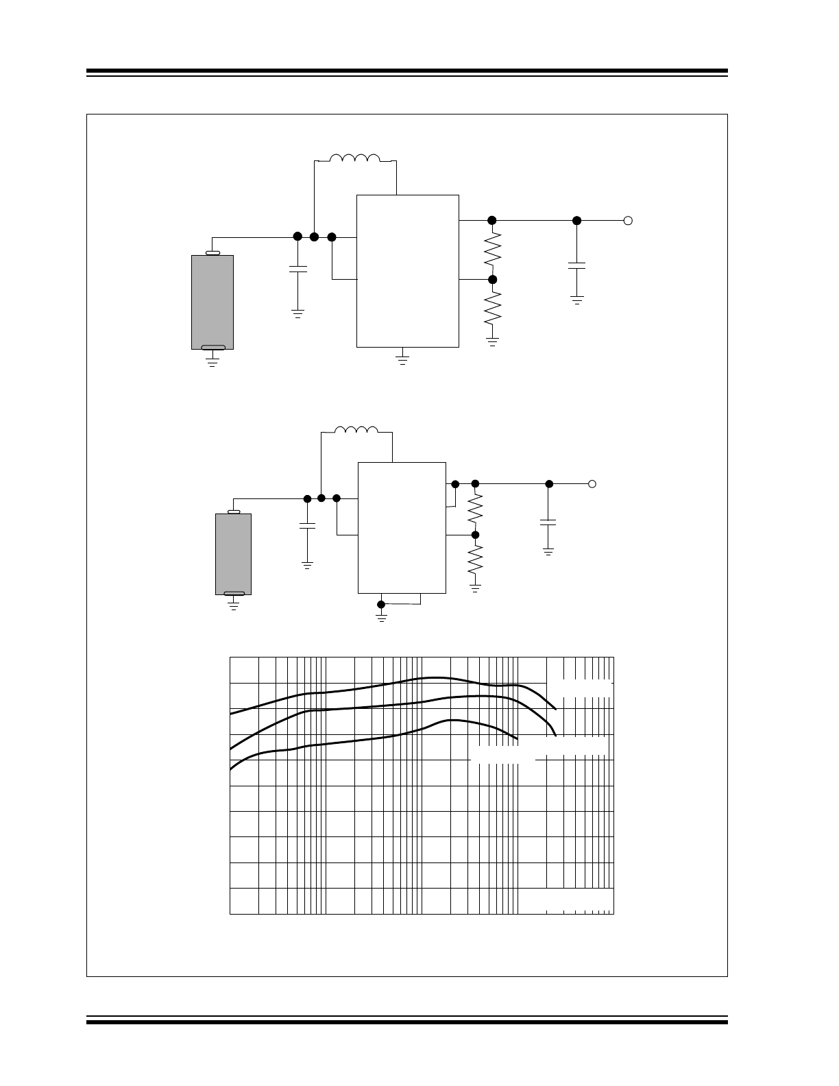
Typical Application
V
IN
P
GND
V
FB
SW
V
IN
3.0V to 4.2V
V
OUT
5.0V / 200 mA
C
OUT
10 µF
C
IN
4.7 µF
L
4.7 µH
V
OUTS
+
-
3.09 M
1 M
V
OUTP
S
GND
Li
-I
on
EN
V
IN
GND
V
FB
SW
V
IN
0.9V to 1.7V
V
OUT
3.3V / 75 mA
C
OUT
10 µF
C
IN
4.7 µF
L
4.7 µH
V
OUT
+
-
1.69 M
1 M
A
lk
a
lin
e
EN
50
55
60
65
70
75
80
85
90
95
100
0.1
1
10
100
1000
Efficiency
(%
)
I
OUT
(mA)
V
OUT
= 3.3V
V
IN
= 1.5V
V
IN
= 2.4V
V
IN
= 3.0V
R
TOP
R
BOT
R
TOP
R
BOT
2013 - 2016 Microchip Technology Inc.
DS20005173B-page 3
MCP16251/2
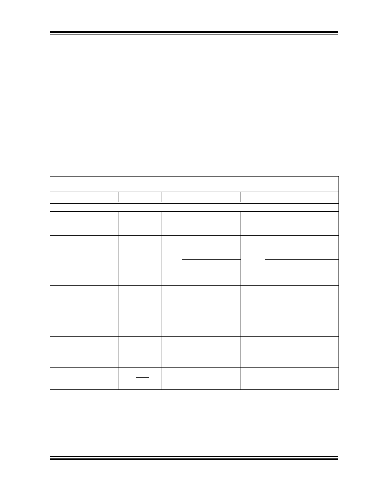
1.0
ELECTRICAL
CHARACTERISTICS
Absolute Maximum Ratings †
EN, V
FB
, V
IN,
V
SW
, V
OUT
- GND ......................... +6.5V
EN, V
FB
.........< maximum V
OUT
or V
IN
> (GND - 0.3V)
Output Short-Circuit Current ...................... Continuous
Output Current Bypass Mode........................... 400 mA
Power Dissipation ............................ Internally Limited
Storage Temperature ......................... -65°C to +150°C
Ambient Temp. with Power Applied...... -40°C to +85°C
Operating Junction Temperature........ -40°C to +125°C
ESD Protection On All Pins:
HBM ............................................................... 4 kV
MM ................................................................ 400V
† Notice: Stresses above those listed under “Maximum
Ratings” may cause permanent damage to the device.
This is a stress rating only and functional operation of
the device at those or any other conditions above those
indicated in the operational sections of this
specification is not intended. Exposure to maximum
rating conditions for extended periods may affect
device reliability.
DC CHARACTERISTICS
Electrical Characteristics: Unless otherwise indicated, V
IN
= 1.5V, C
OUT
= C
IN
= 10 µF, L = 4.7 µH, V
OUT
= 3.3V,
I
OUT
= 0 mA, T
A
= +25°C. Boldface specifications apply over the T
A
range of -40°C to +85°C.
Parameters
Sym.
Min.
Typ.
Max.
Units
Conditions
Input Characteristics
Minimum Start-Up Voltage
V
IN
—
0.82
—
V
Note 1
Minimum Input Voltage
After Start-Up
V
IN
—
0.35
—
V
Note 1
Output Voltage Adjust
Range
V
OUT
1.8
—
5.5
V
V
OUT
V
IN
Note 2
Maximum Output Current
I
OUT
100
150
—
mA
1.2V V
IN
, 2.0V V
OUT
125
—
1.5V V
IN
, 3.3V V
OUT
225
—
3.3V V
IN
, 5.0V V
OUT
Feedback Voltage
V
FB
1.1931
1.23
1.2669
V
Feedback Input
Bias Current
I
VFB
—
10
—
nA
V
OUT
Quiescent Current
I
QOUT
—
4.0
8
µA
I
OUT
= 0 mA, device is not
switching, EN = V
IN
= 4.0V,
V
OUT
= 5.0V, does not
include feedback divider
current (
Note 3
)
V
IN
Sleep Current
I
QIN
—
1.0
2.3
µA
I
OUT
= 0 mA, EN = V
IN
(
Note 3
), (
Note 5
)
No Load Input Current
I
IN0
—
14
25
µA
I
OUT
= 0 mA,
device is switching
Quiescent Current –
Shutdown
I
QSHDN
—
0.6
—
µA
V
OUT
= EN = GND;
includes N-Channel and
P-Channel Switch Leakage
Note 1:
3.3 k
resistive load, 3.3V
OUT
(1 mA).
2:
For V
IN
> V
OUT
, V
OUT
will not remain in regulation.
3:
I
QOUT
is measured at V
OUT,
V
OUT
is supplied externally for V
OUT
> V
IN
(device is not switching), I
QIN
is
measured at V
IN
pin during Sleep period, no load.
4:
220
resistive load, 3.3V
OUT
(15 mA).
5:
Determined by characterization, not production tested.
MCP16251/2
DS20005173B-page 4
2013 - 2016 Microchip Technology Inc.
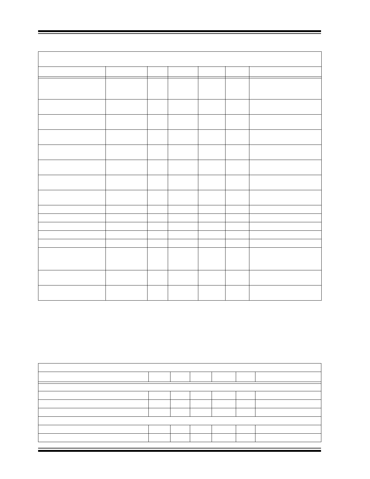
NMOS Switch Leakage
I
NLK
—
0.15
—
µA
V
IN
= V
SW
= 5V
V
OUT
= 5.5V
V
EN
= V
FB
= GND
PMOS Switch Leakage
I
PLK
—
0.15
—
µA
V
IN
= V
SW
= GND
V
OUT
= 5.5V
NMOS Switch
ON Resistance
R
DS(ON)N
—
0.45
—
V
IN
= 3.3V
I
SW
= 100 mA
PMOS Switch
ON Resistance
R
DS(ON)P
—
0.9
—
V
IN
= 3.3V
I
SW
= 100 mA
NMOS Peak
Switch Current Limit
I
N(MAX)
—
650
—
mA
Note 5
V
OUT
Accuracy
V
OUT
%
-3
—
+3
%
Includes Line and Load
Regulation; V
IN
= 1.5V
Line Regulation
(V
OUT
/V
OUT
)
/
V
IN
-0.4
0.3
0.4
%/V
V
IN
= 1.5V to 2.8V
I
OUT
= 50 mA
Load Regulation
V
OUT
/V
OUT
-1.5
0.1
1.5
%
I
OUT
= 25 mA to 100 mA
V
IN
= 1.5V
Maximum Duty Cycle
DC
MAX
87
89
91
%
Note 5
Switching Frequency
f
SW
425
500
575
kHz
EN Input Logic High
V
IH
70
—
—
% of V
IN
I
OUT
= 1 mA
EN Input Logic Low
V
IL
—
—
20
% of V
IN
I
OUT
= 1 mA
EN Input Leakage Current
I
ENLK
—
5.0
—
nA
V
EN
= 5V
Soft Start Time
t
SS
—
—
1.5
ms
EN Low to High
90% of V
OUT
(
Note 4
), (
Note 5
)
Thermal Shutdown
Die Temperature
T
SD
—
160
—
C
I
OUT
= 20 mA
V
IN
> 1.4V
Die Temperature
Hysteresis
T
SDHYS
—
20
—
C
DC CHARACTERISTICS (CONTINUED)
Electrical Characteristics: Unless otherwise indicated, V
IN
= 1.5V, C
OUT
= C
IN
= 10 µF, L = 4.7 µH, V
OUT
= 3.3V,
I
OUT
= 0 mA, T
A
= +25°C. Boldface specifications apply over the T
A
range of -40°C to +85°C.
Parameters
Sym.
Min.
Typ.
Max.
Units
Conditions
Note 1:
3.3 k
resistive load, 3.3V
OUT
(1 mA).
2:
For V
IN
> V
OUT
, V
OUT
will not remain in regulation.
3:
I
QOUT
is measured at V
OUT,
V
OUT
is supplied externally for V
OUT
> V
IN
(device is not switching), I
QIN
is
measured at V
IN
pin during Sleep period, no load.
4:
220
resistive load, 3.3V
OUT
(15 mA).
5:
Determined by characterization, not production tested.
TEMPERATURE SPECIFICATIONS
Electrical Characteristics: Unless otherwise indicated, V
IN
= 1.5V, C
OUT
= C
IN
= 10 µF, L = 4.7 µH, V
OUT
= 3.3V, I
OUT
= 0 mA.
Parameters
Sym.
Min.
Typ.
Max.
Units
Conditions
Temperature Ranges
Operating Temperature Range
T
J
-40
—
+85
°C
Steady State
Storage Temperature Range
T
A
-65
—
+150
°C
Maximum Junction Temperature
T
J
—
—
+150
°C
Transient
Package Thermal Resistances
Thermal Resistance, SOT-23, 6-LD
JA
—
190.5
—
°C/W
EIA/JESD51-3 Standard
Thermal Resistance, TDFN, 2x3x0.8m, 8-LD
JA
—
52.5
—
°C/W
2013 - 2016 Microchip Technology Inc.
DS20005173B-page 5
MCP16251/2
2.0
TYPICAL PERFORMANCE CURVES
Note: Unless otherwise indicated, V
IN
= EN = 1.5V, C
OUT
= C
IN
= 10 µF, L
= 4.7 µH, V
OUT
= 3.3V, I
LOAD
= 0 mA,
T
A
= +25°C, SOT-23 package.
FIGURE 2-1:
V
OUT
I
Q
vs. Ambient
Temperature.
FIGURE 2-2:
No Load Input Current vs.
Temperature.
FIGURE 2-3:
No Load Input Current vs.
V
IN
, after Start-Up.
FIGURE 2-4:
2.0V V
OUT
Efficiency vs.
I
OUT
.
FIGURE 2-5:
3.3V V
OUT
Efficiency vs.
I
OUT
.
FIGURE 2-6:
5.0V V
OUT
Efficiency vs.
I
OUT
.
Note:
The graphs and tables provided following this note are a statistical summary based on a limited number of
samples and are provided for informational purposes only. The performance characteristics listed herein
are not tested or guaranteed. In some graphs or tables, the data presented may be outside the specified
operating range (e.g., outside specified power supply range) and therefore outside the warranted range.
4
6
8
10
s
cent Current (uA)
V
OUT
= 3.3V
R
TOP
= 1.69 M
ȍ
R
BOT
= 1.0 M
ȍ
0
2
-40
-25
-10
5
20
35
50
65
80
Quie
s
Ambient Temperature (°C)
0
5
10
15
20
25
30
-40 -30 -20 -10 0
10 20 30 40 50 60 70 80
No Load Input Current (µA)
Ambient Temperature (°C)
V
IN
= 3.0V
V
IN
= 1.5V
V
OUT
= 3.3V
R
TOP
= 1.69 M
ȍ
R
BOT
= 1.0 M
ȍ
V
IN
= 1.2V
0
5
10
15
20
25
30
35
1
1.5
2
2.5
3
3.5
4
4.5
No Load Input Current (µA)
Input Voltage (V)
R
BOT
= 1.0 M
ȍ
V
OUT
= 3.3V
V
OUT
= 5.0V
V
OUT
= 2.0V
50
55
60
65
70
75
80
85
90
95
100
1
10
100
1000
Efficiency
(%
)
I
OUT
(mA)
V
OUT
= 2.0V
V
IN
= 0.9V
V
IN
= 1.2V
V
IN
= 1.5V
55
60
65
70
75
80
85
90
95
100
1
10
100
1000
Efficiency
(%
)
I
OUT
(mA)
V
OUT
= 3.3V
V
IN
= 0.9V
V
IN
= 1.2V
V
IN
= 2.5V
60
65
70
75
80
85
90
95
100
1
10
100
1000
Efficiency
(%
)
I
OUT
(mA)
V
OUT
= 5.0V
V
IN
= 1.2V
V
IN
= 1.8V
V
IN
= 2.5V
V
IN
= 3.6V
MCP16251/2
DS20005173B-page 6
2013 - 2016 Microchip Technology Inc.
Note: Unless otherwise indicated, V
IN
= EN = 1.5V, C
OUT
= C
IN
= 10 µF, L
= 4.7 µH, V
OUT
= 3.3V, I
LOAD
= 0 mA,
T
A
= +25°C, SOT-23 package.
FIGURE 2-7:
3.3V V
OUT
vs. Ambient
Temperature.
FIGURE 2-8:
3.3V V
OUT
vs. Ambient
Temperature.
FIGURE 2-9:
3.3V V
OUT
vs. V
IN
.
FIGURE 2-10:
Maximum I
OUT
vs. V
IN
, after
Start-up, V
OUT
Maximum 5% below Regulation
Point.
FIGURE 2-11:
F
OSC
vs. Ambient
Temperature.
FIGURE 2-12:
V
IN
Start-Up vs.
Temperature into Resistive Load and Constant
Current.
3 29
3.30
3.31
3.32
3.33
tput V
o
ltage
(V)
I
LOAD
= 1 mA
I
LOAD
= 10 mA
I
LOAD
= 50 mA
3.27
3.28
3.29
-40
-25
-10
5
20
35
50
65
80
Ou
t
Ambient Temperature (°C)
3.28
3.29
3.30
3.31
3.32
u
tput V
o
ltage
(V)
V
IN
= 1.2V
V
IN
= 1.5V
V
= 2 4V
3.25
3.26
3.27
-40
-25
-10
5
20
35
50
65
80
O
u
Ambient Temperature (°C)
I
LOAD
= 20 mA
V
IN
= 0.9V
V
IN
= 2.4V
3.26
3.27
3.28
3.29
3.30
3.31
3.32
3.33
1.5 1.6 1.7 1.8 1.9 2 2.1 2.2 2.3 2.4 2.5 2.6 2.7 2.8
Output V
o
ltage
(V)
Input Voltage (V)
I
LOAD
= 50 mA
T
A
= +25°C
T
A
= +85°C
T
A
= -40°C
0
50
100
150
200
250
300
350
400
450
500
0.9 1.2 1.5 1.8 2.1 2.4 2.7
3
3.3 3.6 3.9 4.2 4.5
Load Current (mA)
Input Voltage (V)
V
OUT
= 3.3V
V
OUT
= 2.0V
V
OUT
= 5.0V
485
490
495
500
505
510
h
ing Frequency
(kHz)
470
475
480
-40
-25
-10
5
20
35
50
65
80
Sw
itc
h
Ambient Temperature (°C)
0 8
0.9
1
1.1
1.2
n
put V
o
ltage
(V)
V
OUT
= 3.3V
---- Electronic Load, CC
Resistive Load
I
LOAD
= 20 mA
0.6
0.7
0.8
-40
-25
-10
5
20
35
50
65
80
In
Ambient Temperature (°C)
I
LOAD
= 1 mA
2013 - 2016 Microchip Technology Inc.
DS20005173B-page 7
MCP16251/2
Note: Unless otherwise indicated, V
IN
= EN = 1.5V, C
OUT
= C
IN
= 10 µF, L
= 4.7 µH, V
OUT
= 3.3V, I
LOAD
= 0 mA,
T
A
= +25°C, SOT-23 package.
FIGURE 2-13:
1.8V
OUT
Minimum Start-Up
and Shutdown V
IN
into Resistive Load vs. I
OUT
.
FIGURE 2-14:
3.3V
OUT
Minimum Start-Up
and Shutdown V
IN
into Resistive Load vs. I
OUT
.
FIGURE 2-15:
5.0V
OUT
Minimum Start-Up
and Shutdown V
IN
into Resistive Load vs. I
OUT
.
FIGURE 2-16:
N-Channel and P-Channel
R
DSON
vs. the Maximum V
IN
or V
OUT
.
FIGURE 2-17:
Average of PFM-to-PWM
Threshold Current vs. V
IN
.
FIGURE 2-18:
MCP16251 3.3V V
OUT
PFM
Mode Waveforms.
0.3
0.5
0.7
0.9
1.1
1.3
0
10
20
30
40
50
60
70
80
90
Input V
o
ltage
(V)
Load Current (mA)
Shutdown
Startup
V
OUT
=1.8V
0.3
0.5
0.7
0.9
1.1
1.3
0
10
20
30
40
50
60
70
80
90
100
Input V
o
ltage
(V)
Load Current (mA)
Shutdown
Startup
V
OUT
= 3.3V
0.3
0.5
0.7
0.9
1.1
1.3
1.5
1.7
0
10
20
30
40
50
60
70
80
90 100
Input V
o
ltage
(V)
Load Current (mA)
Shutdown
Startup
V
OUT
= 5.0V
3
4
5
6
7
8
h
Resistance
(Ohms)
P - Channel
0
1
2
0.9 1.2 1.5 1.8 2.1 2.4 2.7
3
3.3 3.6 3.9 4.2
Sw
itc
h
> V
IN
or V
OUT
N - Channel
20
25
30
35
40
45
ad Current (mA)
V
OUT
= 5.0V
V
OUT
= 3.3V
V
OUT
= 2.0V
5
10
15
0.8
1.2
1.6
2
2.4
2.8
3.2
3.6
4
4.4
Lo
Input Voltage (V)
V
OUT
100 mV/div
AC Coupled
I
OUT
= 1 mA
I
L
100 mA/div
V
SW
200 µs/div
2 V/div
MCP16251/2
DS20005173B-page 8
2013 - 2016 Microchip Technology Inc.
Note: Unless otherwise indicated, V
IN
= EN = 1.5V, C
OUT
= C
IN
= 10 µF, L
= 4.7 µH, V
OUT
= 3.3V, I
LOAD
= 0 mA,
T
A
= +25°C, SOT-23 package.
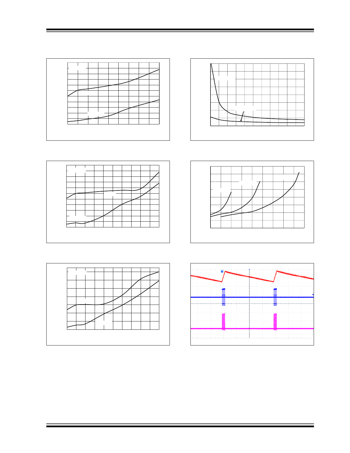
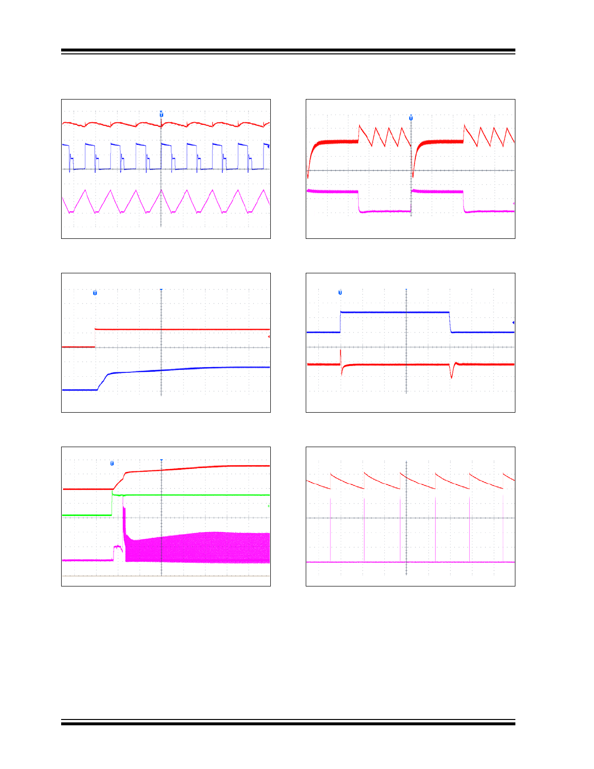
FIGURE 2-19:
MCP16251 3.3V V
OUT
PWM Mode Waveforms.
FIGURE 2-20:
3.3V Start-up after Enable.
FIGURE 2-21:
3.3V Start-Up when
V
IN
= V
ENABLE
.
FIGURE 2-22:
MCP16251 3.3V V
OUT
Load
Transient Waveforms.
FIGURE 2-23:
3.3V V
OUT
Line Transient
Waveforms.
FIGURE 2-24:
MCP16251 3.3V No Load
V
OUT
PFM Mode Output Ripple.
V
OUT
50 mV/div
I
OUT
= 50 mA
I
L
200 mA/div
V
SW
2 µs/div
2 V/div
AC Coupled
V
OUT
= 3.3V
V
IN
= 1.5V
I
OUT
= 15 mA
V
OUT
2 V/div
V
EN
400 µs/div
2 V/div
V
OUT
2V/div
I
OUT
= 15 mA
I
L
100 mA/div
400 µs/div
1 V/div
V
IN
= EN
V
OUT
100 mV/div
AC Coupled
I
STEP
= 1 mA to 75 mA
I
OUT
50 mA/div
400 µs/div
PFM Mode
PWM Mode
V
STEP
from 1V to 2.5V
I
OUT
= 20 mA
V
OUT
100 mV/div
1 ms/div
AC Coupled
V
IN
1 V/div
V
OUT
100 mV/div
AC Coupled
I
OUT
= 0 mA
I
L
20 mA/div
100 ms/div
2013 - 2016 Microchip Technology Inc.
DS20005173B-page 9
MCP16251/2
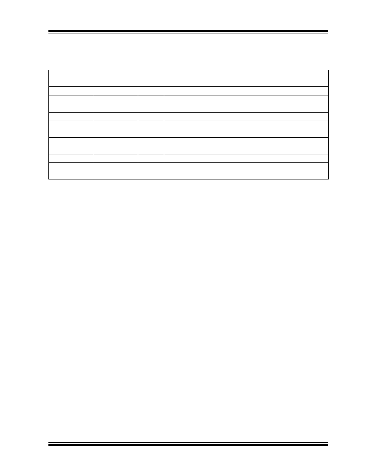
3.0
PIN DESCRIPTIONS
The descriptions of the pins are listed in
Table 3-1
.
3.1
Feedback Voltage Pin (V
FB
)
The V
FB
pin is used to provide output voltage regulation
by using a resistor divider. Feedback voltage will
typically be 1.23V, with the output voltage in regulation.
3.2
Signal Ground Pin (S
GND
)
The signal ground pin is used as a return for the
integrated V
REF
and error amplifier. In the 2x3x0.8
TDFN package, the S
GND
and power ground (P
GND
)
pins are connected externally.
3.3
Power Ground Pin (P
GND
)
The power ground pin is used as a return for the
high-current N-Channel switch. In the 2x3x0.8 TDFN
package, the P
GND
and signal ground (S
GND
) pins are
connected externally.
3.4
Enable Pin (EN)
The EN pin is a logic-level input used to enable or
disable device switching and lower quiescent current
while disabled. A logic high (>70%
of V
IN
) will enable
the regulator output. A logic low (<20% of V
IN
) will
ensure that the regulator is disabled.
3.5
Switch Node Pin (SW)
Connect the inductor from the input voltage to the SW
pin. The SW pin carries inductor current and can be as
high as 650 mA typical peak. The integrated
N-Channel switch drain and integrated P-Channel
switch source are internally connected at the SW node.
3.6
Output Voltage Power Pin (V
OUTP
)
The output voltage power pin connects the output volt-
age to the switch node. High current flows through the
integrated P-Channel and out of this pin to the output
capacitor and output. In the 2x3x0.8 TDFN package,
V
OUTS
and V
OUTP
are connected externally.
3.7
Output Voltage Sense Pin (V
OUTS
)
The output voltage sense pin connects the regulated
output voltage to the internal bias circuits. In the
2x3x0.8 TDFN package, V
OUTS
and V
OUTP
are
connected externally.
3.8
Power Supply Input Voltage Pin (V
IN
)
Connect the input voltage source to V
IN
. The input
source should be decoupled to GND with a 4.7 µF
minimum capacitor.
3.9
Exposed Thermal Pad (EP)
There is no internal electrical connection between the
Exposed Thermal Pad (EP) and the P
GND
and S
GND
pins. They must be connected to the same potential on
the Printed Circuit Board (PCB).
3.10
Ground Pin (GND)
The ground or return pin is used for circuit ground
connection. Length of trace from input cap return,
output cap return and GND pin should be made as
short as possible to minimize noise on the GND pin. In
the SOT23-6 package, a single ground pin is used.
3.11
Output Voltage Pin (V
OUT
)
The output voltage pin connects the integrated
P-Channel MOSFET to the output capacitor. The
feedback voltage divider is also connected to the V
OUT
pin for voltage regulation.
TABLE 3-1:
PIN FUNCTION TABLE
MCP16251/2
SOT-23
MCP16251/2
TDFN 2x3x0.8
Symbol
Description
4
1
V
FB
Feedback Voltage Pin
—
2
S
GND
Signal Ground Pin
—
3
P
GND
Power Ground Pin
3
4
EN
Enable Control Input Pin
1
5
SW
Switch Node, Boost Inductor Input Pin
—
6
V
OUTP
Output Voltage Power Pin
—
7
V
OUTS
Output Voltage Sense Pin
6
8
V
IN
Input Voltage Pin
—
9
EP
Exposed Thermal Pad (EP); must be connected to S
GND
and P
GND.
2
—
GND
Ground Pin
5
—
V
OUT
Output Voltage Pin
MCP16251/2
DS20005173B-page 10
2013 - 2016 Microchip Technology Inc.
4.0
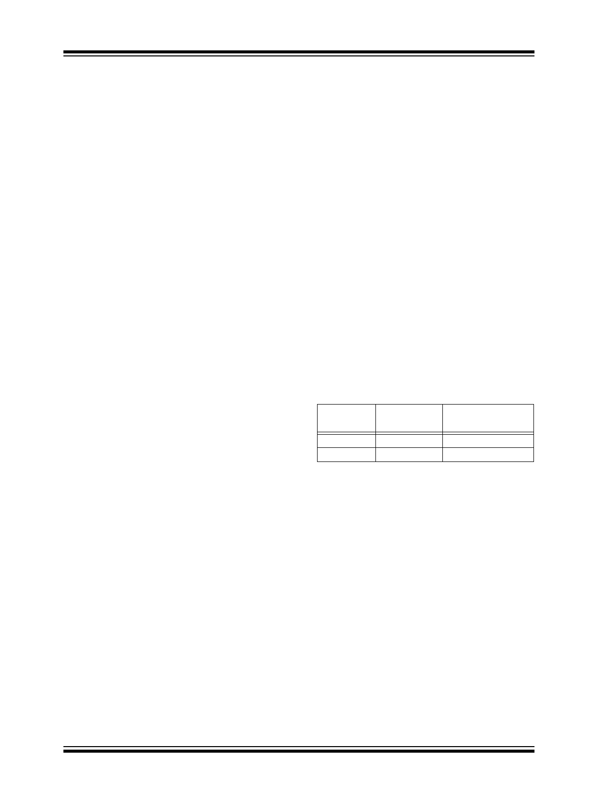
DETAILED DESCRIPTION
4.1
Device Overview
The MCP16251/2 family of devices is capable of low
start-up voltage and delivers high efficiency over a wide
load range for single-cell, two-cell, three-cell alkaline,
NiMH, NiCd and single-cell Li-Ion battery inputs. A high
level of integration lowers total system cost, eases
implementation and reduces board area. The devices
feature low quiescent current, low start-up voltage,
adjustable output voltage, PWM/PFM mode operation,
integrated synchronous switch, internal compensation,
low noise anti-ring control, inrush current limit and soft
start. There are two options for the MCP16251/2 family:
True Output Disconnect and Input-to-Output Bypass
(see
Table 4-1
).
4.1.1
PFM/PWM OPERATION
The MCP16251/2 devices use an automatic switchover
from PWM to PFM mode for light load conditions, to
maximize efficiency over a wide range of output
current. During PFM mode, a controlled peak current is
used to pump the output up to the threshold limit. While
operating in PFM or PWM mode, the P-Channel switch
is used as a synchronous rectifier, turning off when the
inductor current reaches 0 mA to maximize efficiency.
In PFM mode, a comparator is used to terminate
switching when the output voltage reaches the upper
threshold limit. Once switching has terminated, the
output voltage will decay or coast down. During this
period, which is called Sleep period, 1 µA is typically
consumed from the input source, which keeps power
efficiency high at light load. PWM/PFM mode has
higher output ripple voltage than PWM mode, and
variable frequency. The PFM mode frequency is a
function of input voltage, output voltage and load. While
in PFM mode, the boost converter periodically pumps
the output with a fixed switching frequency of 500 kHz.
Figure 2-17
represents the load current versus input
voltage for the PFM-to-PWM threshold.
4.1.2
TRUE OUTPUT DISCONNECT
OPTION
The MCP16251 device incorporates a true output
disconnect feature. With the EN pin pulled low, the
output of the MCP16251 is isolated or disconnected
from the input by turning off the integrated P-Channel
switch and removing the switch bulk diode connection.
This removes the DC path typical in boost converters,
which allows the output to be disconnected from the
input. During this mode, less than 0.6 µA of current is
consumed from the input (battery). True output discon-
nect does not discharge the output; the output voltage
is held up by the external C
OUT
capacitance.
4.1.3
INPUT BYPASS OPTION
The MCP16252 device incorporates the input-to-output
bypass shutdown option. With the EN input pulled low,
the output is connected to the input using the internal
P-Channel MOSFET. In this mode, the current draw
from the input (battery) is less than 0.6 µA with no load.
The Input Bypass mode is used when the input voltage
range is high enough for the load to operate in Standby
or Low I
Q
mode. When a higher regulated output
voltage is necessary to operate the application, the EN
input is pulled high, enabling the boost converter.
In this mode, the current through the P-Channel
MOSFET must not be higher than 400 mA.
TABLE 4-1:
PART NUMBER SELECTION
Part
Number
True Output
Disconnect
Input-to-Output
Bypass
MCP16251
✓
—
MCP16252
—
✓