

2007-2012 Microchip Technology Inc.
DS22042B-page 1
MCP1603/B/L
Features
• Over 90% Typical Efficiency
• Output Current Up To 500 mA
• Low PFM Quiescent Current = 45 µA, typical
(MCP1603/L)
• Low Shutdown Current = 0.1 µA, typical
• Adjustable Output Voltage:
- 0.8V to 4.5V
• Fixed Output Voltage:
- 1.2V, 1.5V, 1.8V, 2.5V, 3.3V (MCP1603/L)
- 1.8V, 3.3V (MCP1603B)
• 2.0 MHz Fixed-Frequency PWM (Heavy Load)
• Automatic PWM-to-PFM Mode Transition
(MCP1603/L)
• PWM Mode Only Option (MCP1603B)
• 100% Duty Cycle Operation
• Internally Compensated
• Undervoltage Lockout (UVLO)
• Overtemperature Protection
• Space Saving Packages:
- 5-Lead TSOT, Two Pinout Types (MCP1603/L)
- 8-Lead 2 x 3 DFN
Applications
• Cellular Telephones
• Portable Computers
• Organizers / PDAs
• USB Powered Devices
• Digital Cameras
• Portable Equipment
• +5V or +3.3V Distributed Systems
• Headsets
General Description
The MCP1603/B/L is a high-efficiency, fully-integrated
500 mA synchronous buck regulator whose 2.7V to
5.5V input voltage range makes it ideally suited for
applications powered from 1-cell Li-Ion or 2-cell/3-cell
NiMH/NiCd batteries.
At heavy loads, the MCP1603/B/L operates in the
2.0 MHz fixed frequency pulse-width modulation
(PWM) mode, which provides a low noise, low-output
ripple, small-size solution. When the load is reduced to
light levels, the MCP1603/L automatically changes
operation to a Pulse Frequency Modulation (PFM)
mode to minimize quiescent current draw from the
battery. No intervention is necessary for a smooth
transition from one mode to another. These two modes
of operation allow the MCP1603/L to achieve the
highest efficiency over the entire operating current
range.
The MCP1603B device disables the PFM mode
switching, and operates only in normal PWM mode
over the entire load range (without skipping).
MCP1603B is for applications that cannot tolerate the
low-frequency output ripple associated with PFM
switching.
The MCP1603/B/L family is available with either an
adjustable or fixed-output voltage. The available fixed
output voltage options for MCP1603/L are 1.2V, 1.5V,
1.8V, 2.5V and 3.3V, and for MCP1603B are 1.8 and
3.3V. When a fixed option is used, only three additional
small external components are needed to form a
complete solution. Couple this with the low profile,
small-foot print packages and the entire system
solution is achieved with minimal size.
Additional protection features include: UVLO,
overtemperature and overcurrent protection.
2.0 MHz, 500 mA Synchronous Buck Regulator
MCP1603/B/L
DS22042B-page 2
2007-2012 Microchip Technology Inc.
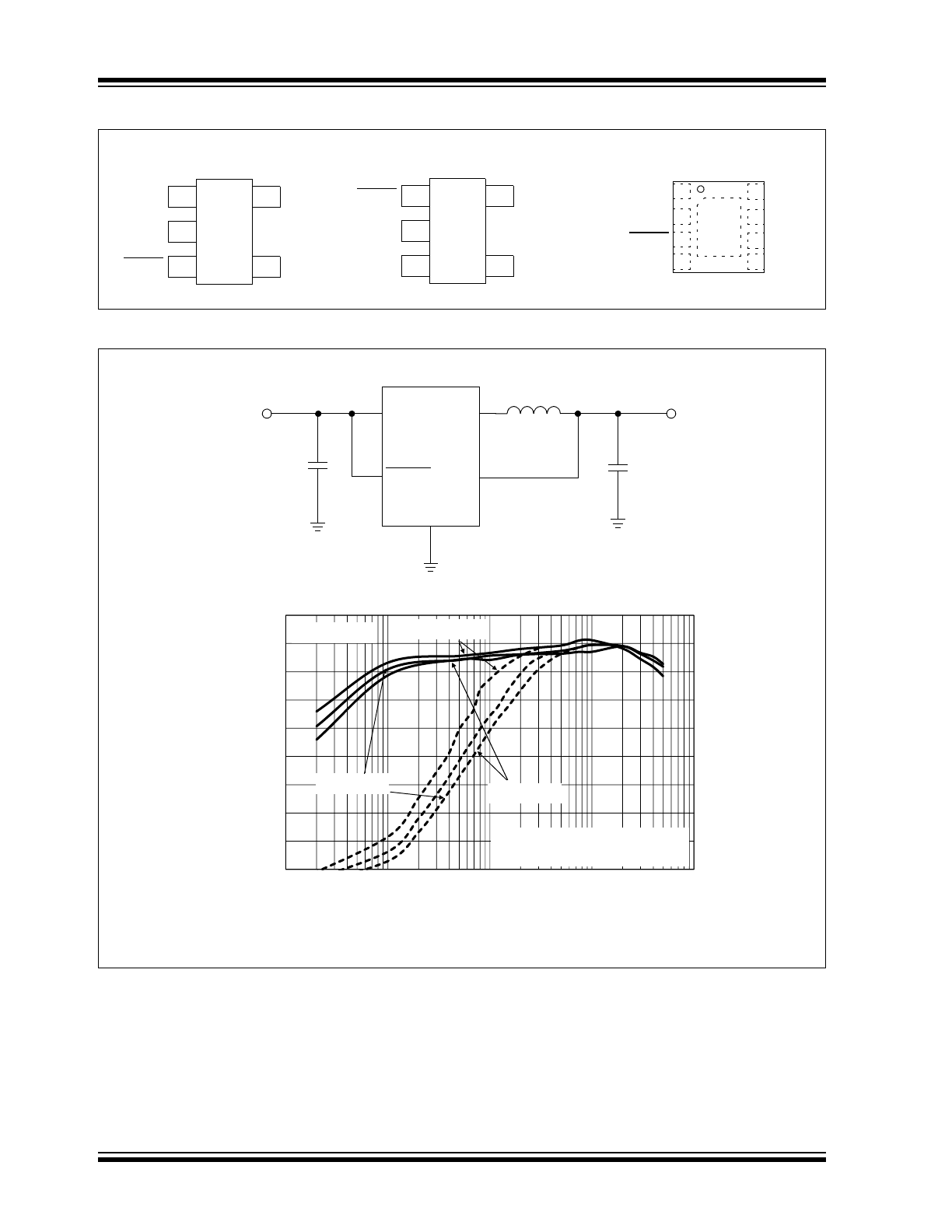
Package Types
Typical Application Circuit
1
2
3
4
5
L
X
V
FB
/V
OUT
SHDN
GND
V
IN
1
2
3
4
5
L
X
V
FB
/V
OUT
SHDN
GND
V
IN
MCP1603/MCP1603B
TSOT
MCP1603L
TSOT
MCP1603
2 x 3 DFN*
SHDN
NC
V
FB
/V
OUT
V
IN
NC
1
2
3
4
8
7
6
5 NC
GND
L
X
* Includes Exposed Thermal Pad (EP); see
Table 3-1
.
EP
9
V
IN
SHDN
GND
V
FB
L
X
V
IN
2.7V to 4.5V
V
OUT
1.8V @ 500 mA
C
OUT
4.7 µF
C
IN
4.7 µF
L
1
4.7 µH
30
40
50
60
70
80
90
100
Efficiency
(%
)
V
OUT
= 1.8V
V
IN
= 2.7V
V
IN
= 3.6V
V
IN
= 4.5V
10
20
30
0.1
1
10
100
1000
Output Current (mA)
__ PFM/PWM (MCP1603/L)
--- PWM (MCP1603B)
2007-2012 Microchip Technology Inc.
DS22042B-page 3
MCP1603/B/L
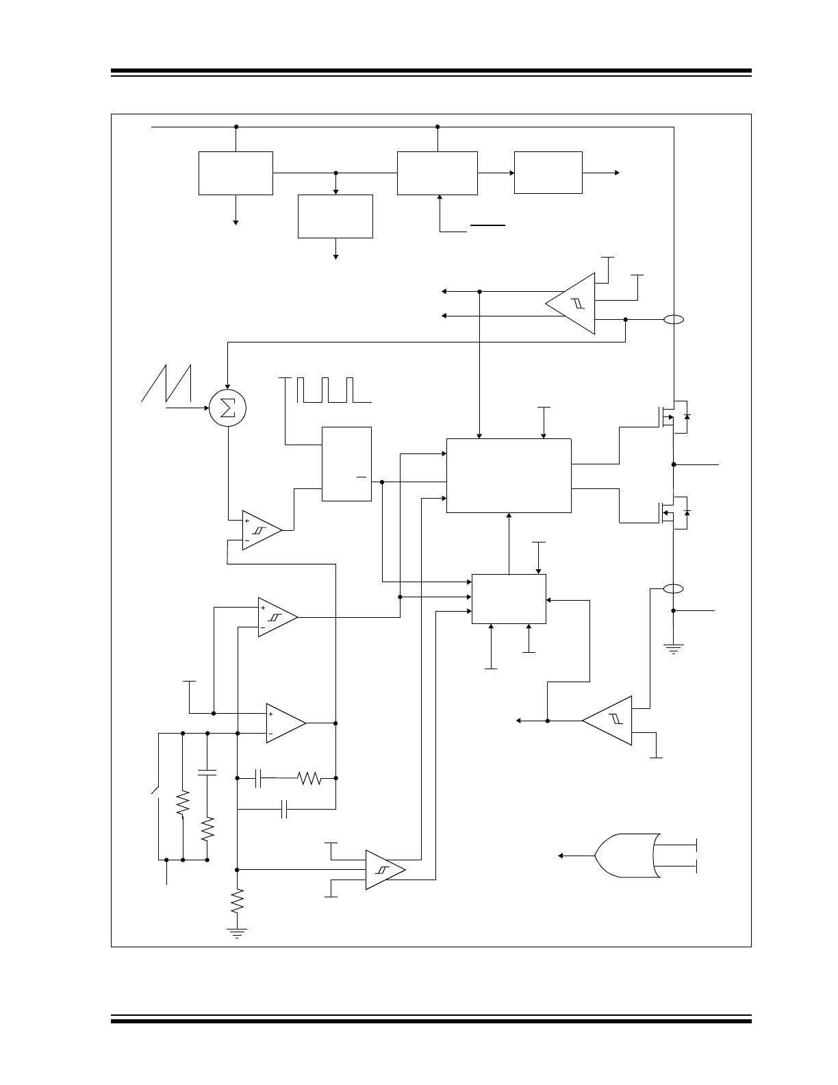
Functional Block Diagram
ILIM
PWM
ILIM
PFM
IPEAK
PWM
IPEAK
PFM
V
IN
SHDN
V
FB
/ V
OUT
GND
L
X
Band
Gap
UVLO
Switch Drive
UVLO
V
REF
Logic and Timing
S
R
Q
Q
Soft Start
V
REF
PWM/PFM
Logic
V
REF
Slope
Comp.
OSC
-I
PK
Limit
UVLO
Thermal
Shutdown
TSD
EA
POFF
NOFF
PWM/PFM - PWM ONLY
TSD
PFM Error Amp
PWM Error Amp
OV Threshold
UV Threshold
I
PK
Limit
-ILPK
IPEAK
PWM
IPEAK
PFM
Disable
Switcher
-ILPK
PWM-ONLY
+
+

MCP1603/B/L
DS22042B-page 4
2007-2012 Microchip Technology Inc.
NOTES:
2007-2012 Microchip Technology Inc.
DS22042B-page 5
MCP1603/B/L
1.0
ELECTRICAL
CHARACTERISTICS
Absolute Maximum Ratings †
V
IN
- GND.......................................................................+6.0V
All Other I/O ............................... (GND - 0.3V) to (V
IN
+ 0.3V)
L
X
to GND .............................................. -0.3V to (V
IN
+ 0.3V)
Output Short Circuit Current ................................. Continuous
Power Dissipation (
Note 5
) .......................... Internally Limited
Storage Temperature ....................................-65°C to +150°C
Ambient Temp. with Power Applied ................-40°C to +85°C
Operating Junction Temperature...................-40°C to +125°C
ESD Protection On All Pins:
HBM ............................................................................. 4 kV
MM ..............................................................................300V
† Notice: Stresses above those listed under "Maximum
Ratings" may cause permanent damage to the device.
This is a stress rating only and functional operation of
the device at those or any other conditions above those
indicated in the operational sections of this specifica-
tion is not intended. Exposure to maximum rating con-
ditions for extended periods may affect device
reliability.
DC CHARACTERISTICS
Electrical Characteristics: Unless otherwise indicated, MCP1603/L, V
IN
= SHDN = 3.6V, C
OUT
= C
IN
= 4.7 µF,
L = 4.7 µH, V
OUT
(ADJ) = 1.8V, I
OUT
= 100 mA, T
A
= +25°C. Boldface specifications apply over the T
A
range of -40°C
to +85°C.
Parameters
Sym
Min
Typ
Max
Units
Conditions
Input Characteristics
Input Voltage
V
IN
2.7
—
5.5
V
Note 1
Maximum Output Current
I
OUT
500
—
—
mA
Note 1
Shutdown Current
I
IN_SHDN
—
0.1
1
µA
SHDN = GND
Quiescent Current - PFM
I
Q
—
45
60
µA
SHDN = V
IN
, I
OUT
= 0 mA,
device switching
Quiescent Current - PWM
I
Q
1.0
2.7
4
mA
SHDN = V
IN
, I
OUT
= 0 mA,
device switching (MCP1603B)
Shutdown/UVLO/Thermal Shutdown Characteristics
SHDN, Logic Input Voltage Low
V
IL
—
—
15
%V
IN
V
IN
= 2.7V to 5.5V
SHDN, Logic Input Voltage High
V
IH
45
—
—
%V
IN
V
IN
= 2.7V to 5.5V
SHDN, Input Leakage Current
I
L_SHDN
-1.0
±0.1
1.0
µA
V
IN
= 2.7V to 5.5V
Undervoltage Lockout
UVLO
2.12
2.28
2.43
V
V
IN
Falling
Undervoltage Lockout Hysteresis
UVLO
HYS
—
140
—
mV
Thermal Shutdown
T
SHD
—
150
—
°C
Note 4
,
Note 5
Thermal Shutdown Hysteresis
T
SHD-HYS
—
10
—
°C
Note 4
,
Note 5
Note 1:
The input voltage should be greater then the output voltage plus headroom voltage; higher load currents
increase the input voltage required for regulation. MCP1603B device requires a minimum load for
regulation. See
Section 2.0, Typical Performance Curves
for typical operating voltage ranges.
2:
Reference Feedback Voltage Tolerance applies to adjustable output voltage setting.
3:
V
R
is the output voltage setting.
4:
The maximum allowable power dissipation is a function of ambient temperature, the maximum allowable
temperature and the thermal resistance from junction to air (i.e. T
A
, T
J
,
JA
). Exceeding the maximum
allowable power dissipation causes the device to initiate thermal shutdown.
5:
The internal MOSFET switches have an integral diode from the L
X
pin to the V
IN
pin, and from the L
X
pin
to the GND pin. In cases where these diodes are forward-biased, the package power dissipation limits
must be adhered to. Thermal protection is not able to limit the junction temperature for these cases.
6:
The current limit threshold is a cycle-by-cycle peak current limit.
MCP1603/B/L
DS22042B-page 6
2007-2012 Microchip Technology Inc.
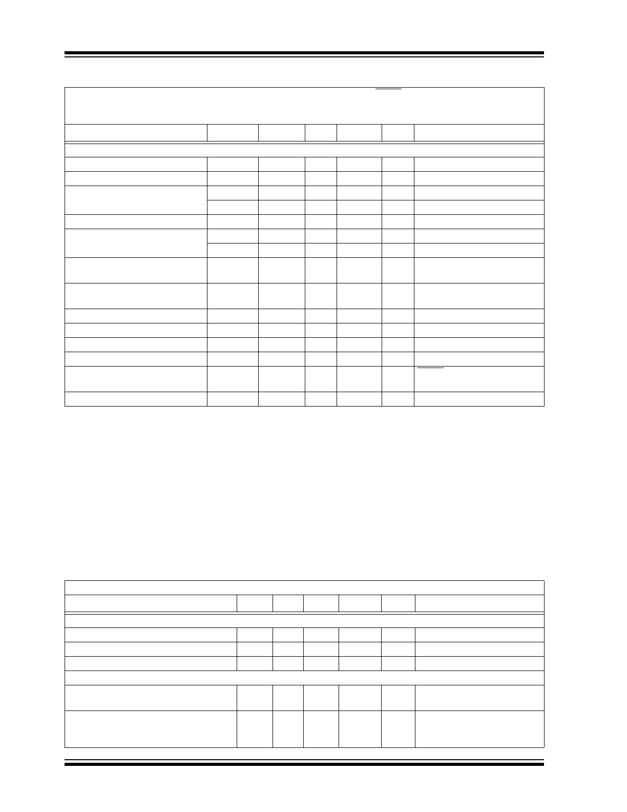
Output Characteristics
Adjustable Output Voltage Range
V
OUT
0.8
—
4.5
V
Note 2
Reference Feedback Voltage
V
FB
—
0.8
—
V
Reference Feedback Voltage
Tolerance
-3.0
—
+3.0
%
T
A
= -40°C to +25°C
-2.5
—
+2.5
%
T
A
= +25°C to +85°C
Feedback Input Bias Current
I
VFB
—
0.1
—
nA
Output Voltage Tolerance Fixed
V
OUT
-3.0%
V
R
+3.0%
%
T
A
= -40°C to +25°C,
Note 3
V
OUT
-2.5
V
R
+2.5
%
T
A
= +25°C to +85°C,
Note 3
Line Regulation
V
LINE-REG
—
0.3
—
%/V
V
IN
= V
R
+ 1V to 5.5V,
I
OUT
= 100 mA
Load Regulation
V
LOAD-REG
—
0.35
—
%
V
IN
= V
R
+1.5V,
I
LOAD
= 100 mA to 500 mA
Internal Oscillator Frequency
F
OSC
1.5
2.0
2.8
MHz
Start Up Time
T
SS
—
0.6
—
ms
T
R
= 10% to 90%
R
DSon
P-Channel
R
DSon-P
—
500
—
m
I
P
= 100 mA
R
DSon
N-Channel
R
DSon-N
—
500
—
m
I
N
= 100 mA
L
X
Pin Leakage Current
I
LX
-1.0
±0.1
1.0
µA
SHDN = 0V, V
IN
= 5.5V,
L
X
= 0V, L
X
= 5.5V
Positive Current Limit Threshold
+I
LX(MAX)
—
860
—
mA
Note 6
TEMPERATURE SPECIFICATIONS
Electrical Specifications: Unless otherwise indicated, all limits are specified for: V
IN
+ 2.7V to 5.5V
Parameters
Sym
Min
Typ
Max
Units
Conditions
Temperature Ranges
Operating Junction Temperature Range
T
J
-40
—
+125
°C
Steady State
Storage Temperature Range
T
A
-65
—
+150
°C
Maximum Junction Temperature
T
J
—
—
+150
°C
Transient
Package Thermal Resistances
Thermal Resistance, 5L-TSOT
JA
—
207.4
—
°C/W
Typical 4-layer Board with
Internal Ground Plane
Thermal Resistance, 8L-2x3 DFN
JA
—
68
—
°C/W
Typical 4-layer Board with
Internal Ground Plane and
2-Vias in Thermal Pad
DC CHARACTERISTICS (CONTINUED)
Electrical Characteristics: Unless otherwise indicated, MCP1603/L, V
IN
= SHDN = 3.6V, C
OUT
= C
IN
= 4.7 µF,
L = 4.7 µH, V
OUT
(ADJ) = 1.8V, I
OUT
= 100 mA, T
A
= +25°C. Boldface specifications apply over the T
A
range of -40°C
to +85°C.
Parameters
Sym
Min
Typ
Max
Units
Conditions
Note 1:
The input voltage should be greater then the output voltage plus headroom voltage; higher load currents
increase the input voltage required for regulation. MCP1603B device requires a minimum load for
regulation. See
Section 2.0, Typical Performance Curves
for typical operating voltage ranges.
2:
Reference Feedback Voltage Tolerance applies to adjustable output voltage setting.
3:
V
R
is the output voltage setting.
4:
The maximum allowable power dissipation is a function of ambient temperature, the maximum allowable
temperature and the thermal resistance from junction to air (i.e. T
A
, T
J
,
JA
). Exceeding the maximum
allowable power dissipation causes the device to initiate thermal shutdown.
5:
The internal MOSFET switches have an integral diode from the L
X
pin to the V
IN
pin, and from the L
X
pin
to the GND pin. In cases where these diodes are forward-biased, the package power dissipation limits
must be adhered to. Thermal protection is not able to limit the junction temperature for these cases.
6:
The current limit threshold is a cycle-by-cycle peak current limit.
2007-2012 Microchip Technology Inc.
DS22042B-page 7
MCP1603/B/L
2.0
TYPICAL PERFORMANCE CURVES
Note: Unless otherwise indicated, MCP1603/L,
V
IN
= SHDN = 3.6V, C
OUT
= C
IN
= 4.7 µF, L = 4.7 µH,
V
OUT
(ADJ) = 1.8V, I
LOAD
= 100 mA, T
A
= +25°C. Adjustable or fixed output voltage options can be used to generate the
Typical Performance Characteristics.
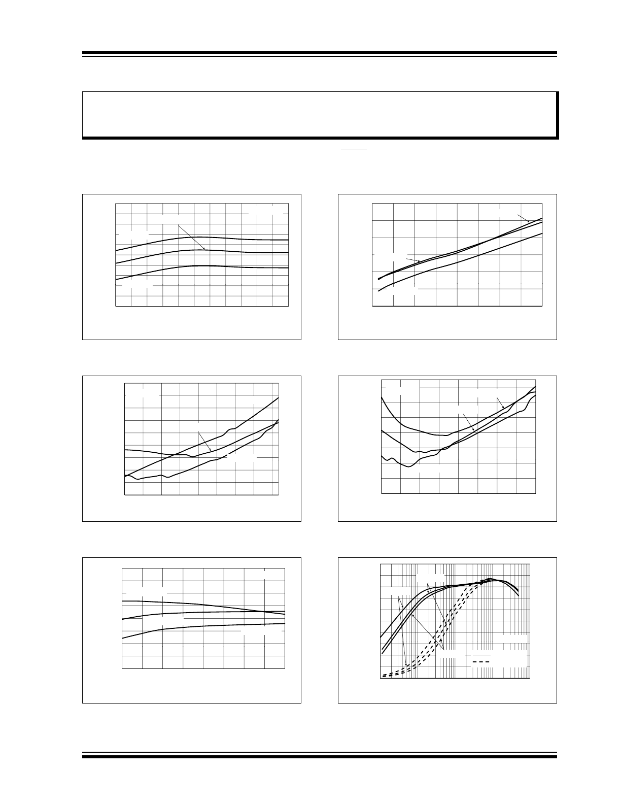
FIGURE 2-1:
PFM I
Q
vs. Ambient
Temperature (MCP1603/L).
FIGURE 2-2:
PWM I
Q
vs. Ambient
Temperature (MCP1603B).
FIGURE 2-3:
Efficiency vs. Input Voltage
(V
OUT
= 1.2V).
FIGURE 2-4:
PFM I
Q
vs. Input Voltage
(MCP1603/L).
FIGURE 2-5:
PWM I
Q
vs. Input Voltage
(MCP1603B).
FIGURE 2-6:
Efficiency vs. Output Load
(V
OUT
= 1.2V).
Note:
The graphs and tables provided following this note are a statistical summary based on a limited number of
samples and are provided for informational purposes only. The performance characteristics listed herein
are not tested or guaranteed. In some graphs or tables, the data presented may be outside the specified
operating range (e.g., outside specified power supply range) and therefore outside the warranted range.
42
43
44
45
46
47
48
49
50
e
scent Current (µA)
V
OUT
= 1.8V
V
IN
= 4.2V
V
= 3 0V
V
IN
= 3.6V
40
41
42
-40 -25 -10
5
20
35
50
65
80
95 110 125
Qui
e
Ambient Temperature (
o
C)
V
IN
= 3.0V
2.7
2.8
2.9
3
3.1
3.2
3.3
s
cent Current (mA)
V
OUT
= 1.8V
V
IN
= 3.0V
V
IN
= 3.6V
V
IN
= 4.2V
2.4
2.5
2.6
2.7
-40
-25
-10
5
20
35
50
65
80
Quie
s
Ambient Temperature (
o
C)
V
IN
3.6V
70
75
80
85
90
95
100
Efficiency
(%
)
V
OUT
= 1.2V
I
OUT
= 100 mA
I
OUT
= 500 mA
I
OUT
= 300 mA
60
65
2.7
3.05
3.4
3.75
4.1
4.45
4.8
5.15
5.5
Input Voltage (V)
44
46
48
50
52
iescent Current (µA)
T
A
= +25
o
C
T
A
= +90
o
C
40
42
2.7
3.05
3.4
3.75
4.1
4.45
4.8
5.15
5.5
Qu
i
Input Voltage (V)
T
A
= -40
o
C
2.6
2.8
3
3.2
3.4
s
cent Current (mA)
T
A
= +25
o
C
T
A
= +90
o
C
V
OUT
= 1.8V
2
2.2
2.4
2.7
3.05
3.4
3.75
4.1
4.45
4.8
5.15
5.5
Quie
s
Input Voltage (V)
T
A
= -40
o
C
30
40
50
60
70
80
90
100
E
fficiency
(%
)
V
OUT
= 1.2V
V
IN
= 2.7V
V
IN
= 3.6V
0
10
20
30
0.1
1
10
100
1000
E
Output Current (mA)
OUT
V
IN
= 4.2V
PFM/PWM
PWM Only
MCP1603/B/L
DS22042B-page 8
2007-2012 Microchip Technology Inc.
Note: Unless otherwise indicated, MCP1603/L,
V
IN
= SHDN = 3.6V, C
OUT
= C
IN
= 4.7 µF, L = 4.7 µH,
V
OUT
(ADJ) = 1.8V, I
LOAD
= 100 mA, T
A
= +25°C. Adjustable or fixed output voltage options can be used to generate the
Typical Performance Characteristics.
FIGURE 2-7:
Efficiency vs. Input Voltage
(V
OUT
= 1.8V).
FIGURE 2-8:
Efficiency vs. Output Load
(V
OUT
= 1.8V).
FIGURE 2-9:
Efficiency vs. Input Voltage
(V
OUT
= 2.4V).
FIGURE 2-10:
Line Regulation vs. Ambient
Temperature (V
OUT
= 1.8V).
FIGURE 2-11:
Output Voltage vs. Load
Current (V
OUT
= 1.8V).
FIGURE 2-12:
PFM/PWM Efficiency vs.
Output Load (V
OUT
= 2.4V).
80
85
90
95
100
Efficiency
(%
)
V
OUT
= 1.8V
I
OUT
= 100 mA
I
OUT
= 500 mA
I
OUT
= 300 mA
70
75
2.7
3.05
3.4
3.75
4.1
4.45
4.8
5.15
5.5
Input Voltage (V)
30
40
50
60
70
80
90
100
E
fficiency
(%
)
V
1 8V
V
IN
= 4.2V
V
IN
= 2.7V
V
IN
= 3.6V
0
10
20
30
0.1
1
10
100
1000
E
Output Current (mA)
V
OUT
= 1.8V
PFM/PWM
PWM Only
80
85
90
95
100
Efficiency
(%
)
V
OUT
= 2.4V
I
OUT
= 100 mA
I
OUT
= 500 mA
I
OUT
= 300 mA
75
80
3
3.5
4
4.5
5
5.5
Input Voltage (V)
0 2
0.3
0.4
0.5
0.6
n
e Regualtion (%
/V)
I
OUT
= 100 mA
I
OUT
= 300 mA
V
OUT
= 1.8V
0.1
0.2
-40 -25 -10
5
20 35 50 65 80 95 110 125
Li
n
Ambient Temperature (
o
C)
1.76
1.77
1.78
1.79
1.80
1.81
1.82
O
utput V
o
ltage
(V)
T
A
= +125
o
C
T
A
= -40
o
C
T
A
= +25
o
C
T
A
= +90
o
C
1.74
1.75
100
150
200
250
300
350
400
450
500
O
Output Current (mA)
30
40
50
60
70
80
90
100
E
fficiency
(%
)
V
2 4V
V
IN
= 4.2V
V
IN
= 2.7V
V
IN
= 3.6V
0
10
20
30
0.1
1
10
100
1000
E
Output Current (mA)
V
OUT
= 2.4V
PFM/PWM
PWM Only
2007-2012 Microchip Technology Inc.
DS22042B-page 9
MCP1603/B/L
Note: Unless otherwise indicated, MCP1603/L,
V
IN
= SHDN = 3.6V, C
OUT
= C
IN
= 4.7 µF, L = 4.7 µH,
V
OUT
(ADJ) = 1.8V, I
LOAD
= 100 mA, T
A
= +25°C. Adjustable or fixed output voltage options can be used to generate the
Typical Performance Characteristics.
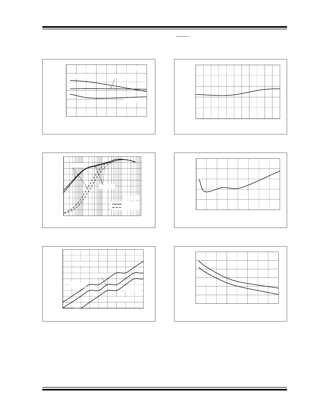
FIGURE 2-13:
Efficiency vs. Input Voltage
(V
OUT
= 3.3V).
FIGURE 2-14:
Efficiency vs. Output Load
(V
OUT
= 3.3V).
FIGURE 2-15:
PWM-Only Device Minimum
Load for Regulation (MCP1603B).
FIGURE 2-16:
Switching Frequency vs.
Ambient Temperature.
FIGURE 2-17:
Switching Frequency vs.
Input Voltage.
FIGURE 2-18:
Switch Resistance vs. Input
Voltage.
90.0
92.5
95.0
97.5
100.0
Efficiency
(%
)
V
OUT
= 3.3V
I
OUT
= 100 mA
I
OUT
= 500 mA
I
OUT
= 300 mA
85.0
87.5
3.5
3.75
4
4.25
4.5
4.75
5
5.25
5.5
Input Voltage (V)
40
50
60
70
80
90
100
E
fficiency
(%
)
V
IN
= 4.2V
V
IN
= 3.6V
0
10
20
30
0.1
1
10
100
1000
E
Output Current (mA)
V
OUT
= 3.3V
PFM/PWM
PWM Only
3
4
5
6
7
8
9
10
o
ad Current (mA)
T
A
= -40
o
C
T
A
= +25
o
C
T
A
= +85
o
C
Regulation
0
1
2
3
1.8
2
2.2
2.4
2.6
2.8
3
3.2
3.4
3.6
L
o
V
IN
- V
OUT
(V)
T
A
= +85 C
No Regulation
2.05
2.10
2.15
2.20
h
ing Frequency
(MHz)
1.95
2.00
-40 -25 -10
5
20 35 50 65 80 95 110 125
Sw
itc
h
Ambient Temperature (
o
C)
2 00
2.05
2.10
2.15
2.20
h
ing Frequency
(MHz)
1.95
2.00
2.7
3.05
3.4
3.75
4.1
4.45
4.8
5.15
5.5
Sw
itc
h
Input Voltage (V)
0.45
0.50
0.55
0.60
0.65
tch Resistance
()
N-Channel
P-Channel
0.35
0.40
2.7 3.05 3.4 3.75 4.1 4.45 4.8 5.15 5.5
Sw
it
Input Voltage (V)
MCP1603/B/L
DS22042B-page 10
2007-2012 Microchip Technology Inc.
Note: Unless otherwise indicated, MCP1603/L,
V
IN
= SHDN = 3.6V, C
OUT
= C
IN
= 4.7 µF, L = 4.7 µH,
V
OUT
(ADJ) = 1.8V, I
LOAD
= 100 mA, T
A
= +25°C. Adjustable or fixed output voltage options can be used to generate the
Typical Performance Characteristics.
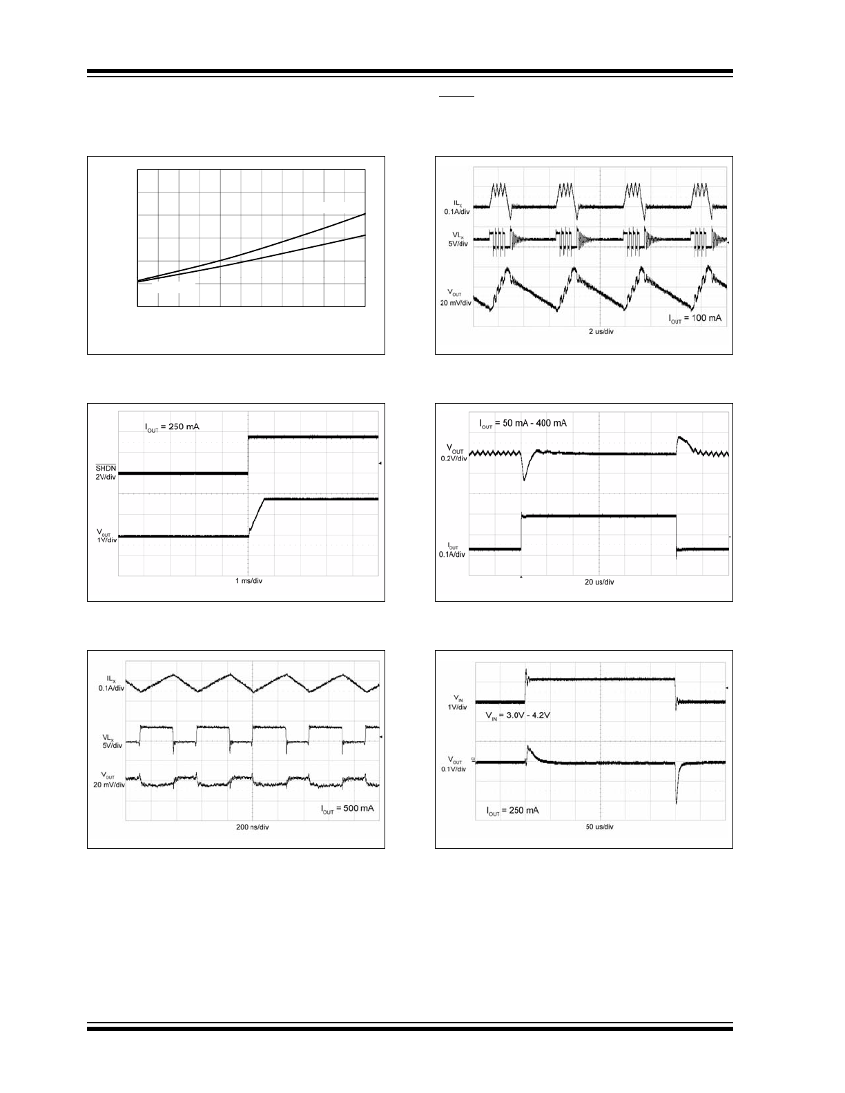
FIGURE 2-19:
Switch Resistance vs.
Ambient Temperature.
FIGURE 2-20:
Output Voltage Startup
Waveform.
FIGURE 2-21:
Heavy Load Switching
Waveform.
FIGURE 2-22:
PFM Light Load Switching
Waveforms (MCP1603/L).
FIGURE 2-23:
Output Voltage Load Step
Response vs. Time.
FIGURE 2-24:
Output Voltage Line Step
Response vs. Time.
0.5
0.6
0.7
0.8
0.9
tch Resistance
()
N-Channel
0.3
0.4
-40 -25 -10 5
20 35 50 65 80 95 110 125
Sw
it
Ambient Temperature (
o
C)
P-Channel