
2015-2017 Microchip Technology Inc.
DS20005474E-page 1
MCP1501
Features
• Maximum Temperature Coefficient: 50 ppm/°C
from –40°C to +125°C
• Initial Accuracy: 0.1%
• Operating Temperature Range: –40 to +125°C
• Low Typical Operating Current: 140 μA
• Line Regulation: 50 ppm/V Maximum
• Load Regulation: 40 ppm/mA Maximum
• 8 Voltage Variants Available:
- 1.024V
- 1.250V
- 1.800V
- 2.048V
- 2.500V
- 3.000V
- 3.300V
- 4.096V
• Output Noise: 27 µVRMS, 10 Hz to 10 kHz
(1.024V)
Applications
• Precision Data Acquisition Systems
• High-Resolution Data Converters
• Medical Equipment Applications
• Industrial Controls
• Battery-Powered Devices
General Description
The MCP1501 is a buffered voltage reference capable
of sinking and sourcing 20 mA of current. The voltage
reference is a low-drift bandgap-based reference. The
bandgap uses chopper-based amplifiers, effectively
reducing the drift to zero.
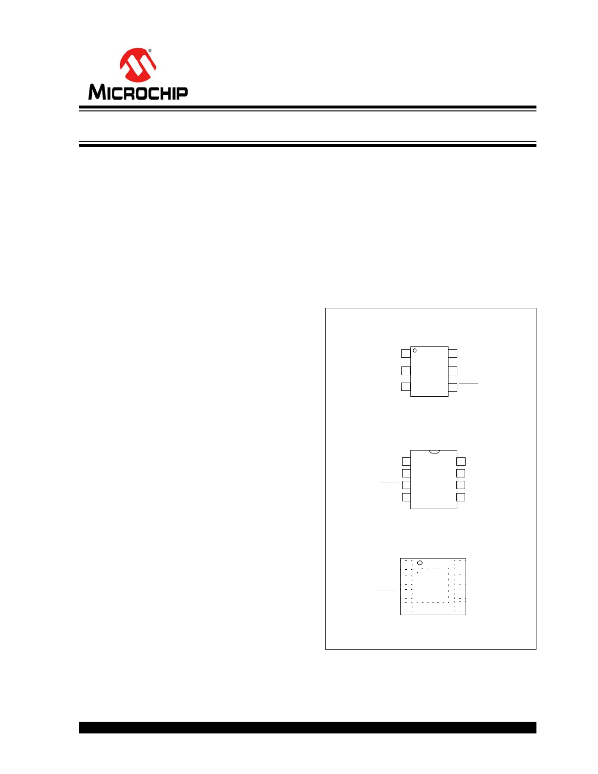
The MCP1501 is available in the following packages:
• 6-Lead SOT-23
• 8-Lead SOIC
• 8-Lead 2 mm x 2 mm WDFN
Package Types
4
1
2
3
6 V
DD
SHDN
OUT
GND
GND
5 GND
MCP1501
6-Lead SOT-23
FEEDBACK
GND
V
DD
GND
SHDN
OUT
MCP1501
8-Lead SOIC
GND
GND
MCP1501
2x2 WDFN*
SHDN
GND
GND
OUT
GND
1
2
3
4
8
7
6
5 GND
FEEDBACK
V
DD
EP
9
*Includes Exposed Thermal Pad (EP). See
Table 3-1
8
7
6
5
1
2
3
4
High-Precision Buffered Voltage Reference
MCP1501
DS20005474E-page 2
2015-2017 Microchip Technology Inc.
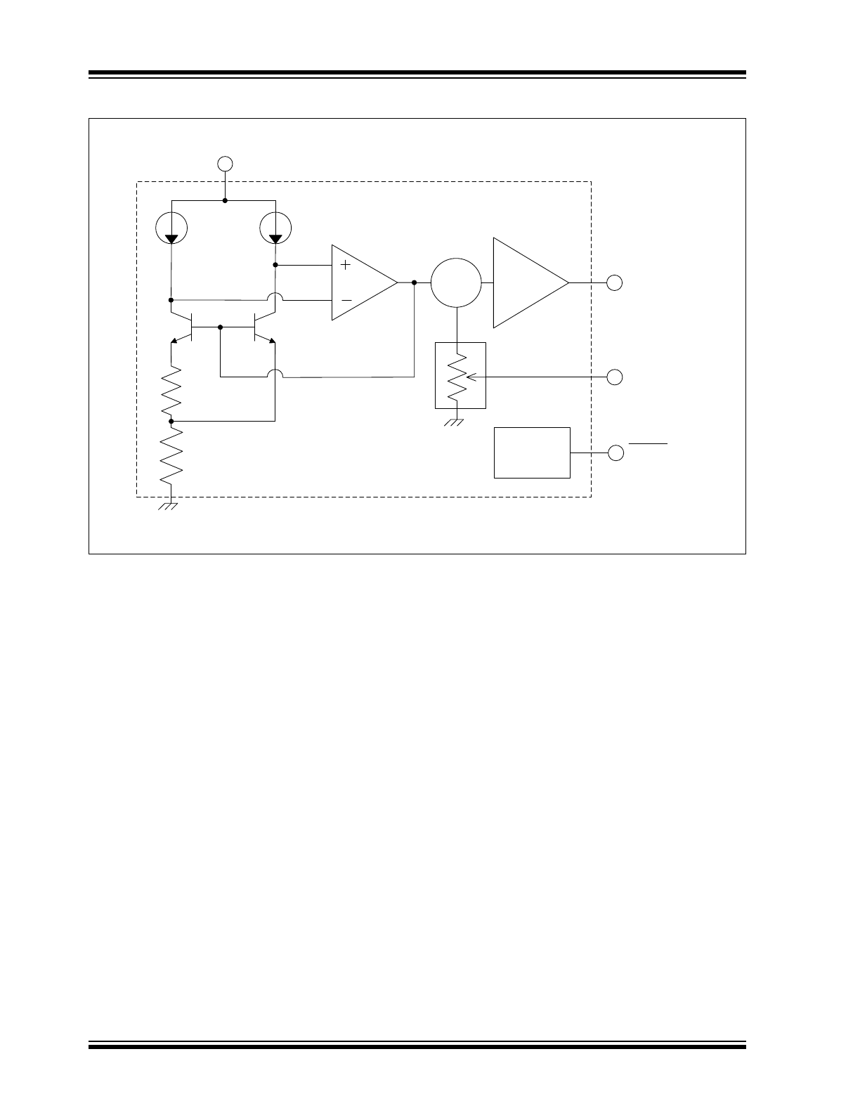
BLOCK DIAGRAM
Shutdown
Circuitry
Σ
OUT
FEEDBACK
SHDN
GND
V
DD
2015-2017 Microchip Technology Inc.
DS20005474E-page 3
MCP1501
1.0
ELECTRICAL CHARACTERISTICS
Absolute Maximum Ratings
(†)
V
DD
.............................................................................................................................................................................5.5V
Maximum current into V
DD
pin ............................................................................................................................... 30 mA
Clamp current, I
K
(V
PIN
< 0 or V
PIN
> V
DD
)...........................................................................................................±20 mA
Maximum output current sunk by OUTPUT pin ......................................................................................................30 mA
Maximum output current sourced by OUTPUT pin .................................................................................................30 mA
(HBM:CDM:MM)................................................................................................................................ (2 kV:±1.5 kV:200V)
† Notice
: Stresses above those listed under “Absolute Maximum Ratings” may cause permanent damage to the
device. This is a stress rating only and functional operation of the device at those or any other conditions above those
indicated in the operation listings of this specification is not implied. Exposure above maximum rating conditions for
extended periods may affect device reliability.
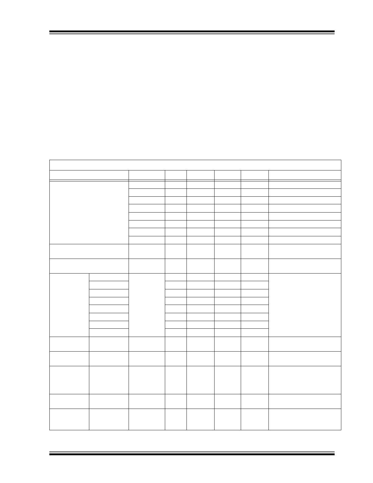
TABLE 1-1:
DC CHARACTERISTICS
Electrical Characteristics:
Unless otherwise specified, V
DD(MIN)
V
DD
5.5V at –40C T
A
+125C.
Characteristic
Sym.
Min.
Typ.
Max.
Units
Conditions
Supply Voltage
V
DD
1.65
—
5.5
V
MCP1501-10
V
DD
1.65
—
5.5
V
MCP1501-12
V
DD
2.0
—
5.5
V
MCP1501-18
V
DD
2.25
—
5.5
V
MCP1501-20
V
DD
2.70
—
5.5
V
MCP1501-25
V
DD
3.2
—
5.5
V
MCP1501-30
V
DD
3.5
—
5.5
V
MCP1501-33
V
DD
4.3
—
5.5
V
MCP1501-40
Power-on-Reset
Release Voltage
V
POR
—
1.45
—
V
Power-on-Reset
Rearm Voltage
—
—
0.8
—
V
Output Voltage MCP1501-10
V
OUT
1.0230
1.0240
1.0250
V
MCP1501-12
1.2488
1.2500
1.2513
V
MCP1501-18
1.7982
1.800
1.8018
V
MCP1501-20
2.0460
2.0480
2.0500
V
MCP1501-25
2.4975
2.500
2.5025
V
MCP1501-30
2.9970
3.000
3.0030
V
MCP1501-33
3.2967
3.300
3.3033
V
MCP1501-40
4.0919
4.0960
4.1001
V
Temperature
Coefficient
MCP1501-XX
T
C
—
10
50
ppm/
C
Line
Regulation
V
OUT
/
V
IN
—
5
50
ppm/V
Load
Regulation
V
OUT
/
I
OUT
—
10 ppm –
sink
15 ppm –
source
40 ppm –
sink
70 ppm –
source
ppm/mA –5 mA < I
LOAD
< +5 mA
Dropout
Voltage
V
DO
—
—
200
mV
–5 mA < I
LOAD
< +2 mA
Power Supply
Rejection
Ratio
PSRR
94 dB
1.024V option, V
IN
= 5.5V,
60 Hz at 100 mV
P-P
MCP1501
DS20005474E-page 4
2015-2017 Microchip Technology Inc.
Shutdown
V
IL
1.35
V
IN
= 5.5V
V
IH
3.80
Output Voltage
Hysteresis
∆V
OUT_HYST
300 µV
Refer to
Section 1.1.10
“Output Voltage
Hysteresis”
for additional
details on testing conditions.
Output Noise
MCP1501-10
e
N
—
14
—
µVRMS
0.1 Hz to 10 Hz, T
A
= +25
C
—
27
—
10 Hz to 10 kHz, T
A
= +25
C
MCP1501-40
e
N
—
20
—
µVRMS
0.1 Hz to 10 Hz, T
A
= +25
C
—
110
—
10 Hz to 10 kHz, T
A
= +25
C
Maximum
Load Current
I
LOAD
—
±20
—
mA
T
A
= +25°C
2.048V option
Supply
Current
I
DD
—
140
550
µA
No Load
—
—
350
No Load, T
A
= +25°C
Shutdown
Current
MCP1501-10
I
SHDN
205 nA
T
A
= +25°C
MCP1501-20
185
MCP1501-40
185
TABLE 1-1:
DC CHARACTERISTICS (CONTINUED)
Electrical Characteristics:
Unless otherwise specified, V
DD(MIN)
V
DD
5.5V at –40C T
A
+125C.
Characteristic
Sym.
Min.
Typ.
Max.
Units
Conditions
TABLE 1-2:
TEMPERATURE SPECIFICATIONS
Electrical Specifications:
Unless otherwise indicated, all parameters apply at AV
DD,
DV
DD
= 2.7 to 3.6V.
Parameters
Sym.
Min.
Typ.
Max.
Units
Conditions
Temperature Ranges
Operating Temperature Range
T
A
–40
—
+125
°C
Storage Temperature Range
T
A
–65
—
+150
°C
Thermal Package Resistance
Thermal Resistance for SOT-23-6
JA
—
+190.5
—
°C/W
Thermal Resistance for SOIC-8
JA
—
+149.5
—
°C/W
Thermal Resistance for DFN-8
JA
—
+141.3
—
°C/W
2015-2017 Microchip Technology Inc.
DS20005474E-page 5
MCP1501
1.1
Terminology
1.1.1
OUTPUT VOLTAGE
Output voltage is the reference voltage that is available
on the OUT pin.
1.1.2
INPUT VOLTAGE
The input voltage (V
IN
) is the range of voltage that can
be applied to the V
DD
pin and still have the device
produce the designated output voltage on the OUT pin.
1.1.3
TEMPERATURE COEFFICIENT
(TC
OUT
)
The output temperature coefficient or voltage drift is a
measure of how much the output voltage will vary from
its initial value with changes in ambient temperature.
The value specified in the electrical specifications is
measured as shown in
Equation 1-1
.
EQUATION 1-1:
TC
OUTPUT
CALCULATION
1.1.4
DROPOUT VOLTAGE
The dropout voltage is defined as the voltage difference
between V
DD
and V
OUT
under load.
Equation 1-2
is
used to calculate the dropout voltage.
EQUATION 1-2:
1.1.5
LINE REGULATION
An ideal voltage reference will maintain a constant out-
put voltage regardless of any changes to the input volt-
age. However, when real devices are considered, a
small error may be measured on the output when an
input voltage change occurs.
Line regulation is defined as the change in output volt-
age (
V
OUT
) as a function of a change in input voltage
(
V
IN
), and expressed as a percentage, as shown in
Equation 1-3
.
EQUATION 1-3:
Line regulation may also be expressed as %/V or in
ppm/V, as shown in
Equation 1-4
and
Equation 1-5
,
respectively.
EQUATION 1-4:
EQUATION 1-5:
As an example, if the MCP1501-20 is implemented in a
design and a 2 µV change in output voltage is mea-
sured from a 250 mV change on the input, then the
error in percent, ppm, percent/volt, and ppm/volt, as
shown in
Equation 1-6
–
Equation 1-9
.
EQUATION 1-6:
EQUATION 1-7:
EQUATION 1-8:
EQUATION 1-9:
TC
OUT
V
OUT MAX
VOUT MIN
–
T
V
OUT NOM
---------------------------------------------------------------------------
10
6
ppm/
C
=
Where:
V
OUT(MAX)
= Maximum output voltage over the
temperature range
V
OUT(MIN)
= Minimum output voltage over the
temperature range
V
OUT(NOM)
= Average output voltage over the
temperature range
T = Temperature range over which the
data was collected
V
DO
V
IN
V
OUT
| I
OUT
Cons
t
tan
=
–
=
V
OUT
V
IN
--------------------
100%
%
Line
Regulation
=
V
OUT
V
OUT NOM
-----------------------------------
V
IN
-----------------------------------------
100%
%
V
----- Line Regulation
=
V
OUT
V
OUT NOM
-----------------------------------
V
IN
-----------------------------------------
10
6
ppm
V
----------- Line Regulation
=
V
OUT
V
IN
--------------------
100%
2
V
250 mV
------------------
100%
.0008%
=
V
OUT
V
IN
--------------------
10
6
2
V
250 mV
------------------
10
6
8 ppm
=
V
OUT
V
IN
--------------------
100%
2
V
2.048V
-----------------
250 mV
-----------------------
100%
0.000390625
%
V
-----
=
=
V
OUT
V
IN
--------------------
10
6
2
V
2.048V
-----------------
250 mV
-----------------------
10
6
3.90625
ppm
V
------------
=
=
MCP1501
DS20005474E-page 6
2015-2017 Microchip Technology Inc.
1.1.6
LOAD REGULATION
An ideal voltage reference will maintain the specified
output voltage regardless of the load's current demand.
However, real devices experience a small error voltage
that deviates from the specified output voltage when a
load is present.
Load regulation is defined as the voltage difference
when under no load (V
OUT
@ I
OUT|0
) and under maxi-
mum load (V
OUT
@ I
OUT|MAX
), and is expressed as a
percentage, as shown in
Equation 1-10
.
EQUATION 1-10:
Similar to line regulation, load regulation may also be
expressed as %/mA or in ppm/mA as shown in
Equation 1-11
and
Equation 1-12
, respectively.
EQUATION 1-11:
EQUATION 1-12:
As an example, if the MCP1501-20 is implemented in a
design and a 10 µV change in output voltage is mea-
sured from a 2 mA change on the input, then the error
in percent, ppm, percent/volt, ppm/volt, as shown in
Equation 1-13
–
Equation 1-16
.
EQUATION 1-13:
EQUATION 1-14:
EQUATION 1-15:
EQUATION 1-16:
V
OUT
@ I
OUT|0
V
OUT
@ I
OUT|MAX
–
V
OUT
@ I
OUT|0
--------------------------------------------------------------------------------------------------------------
100%
% Load Regulation
=
V
OUT
V
OUT NOM
-----------------------------------
I
OUT
-----------------------------------------
100%
%
mA
-------- Load Regulation
=
V
OUT
V
OUT NOM
-----------------------------------
I
OUT
-----------------------------------------
10
6
ppm
mA
----------- Load Regulation
=
2.048V
2.04799V
–
2.04799V
-----------------------------------------------
100% .
=
0004882%
2.048V
2.04799V
–
2.04799V
-----------------------------------------------
10
6
2.048V
2.04799V
–
2.04799V
----------------------------------------------- 10
6
=
4.882 ppm
=
V
OUT
V
OUT NOM
------------------------------------
I
OUT
------------------------------------------ 100%
10
V
2.048V
-----------------
2 mA
-----------------------
100%
0.2441
%
mA
--------
=
=
V
OUT
V
OUT NOM
------------------------------------
I
OUT
------------------------------------------ 10
6
10
V
2.048V
-----------------
2 mA
-----------------------
10
6
2.441
ppm
mA
-----------
=
=
2015-2017 Microchip Technology Inc.
DS20005474E-page 7
MCP1501
1.1.7
INPUT CURRENT
The input current (operating current) is the current that
sinks from V
IN
to GND without a load current on the
output pin. This current is affected by temperature,
input voltage, output voltage, and the load current.
1.1.8
POWER SUPPLY REJECTION
RATIO
Power supply rejection ratio (PSRR) is a measure of
the change in output voltage (∆V
OUT
) relative to the
change in input voltage (∆V
IN
) over frequency.
1.1.9
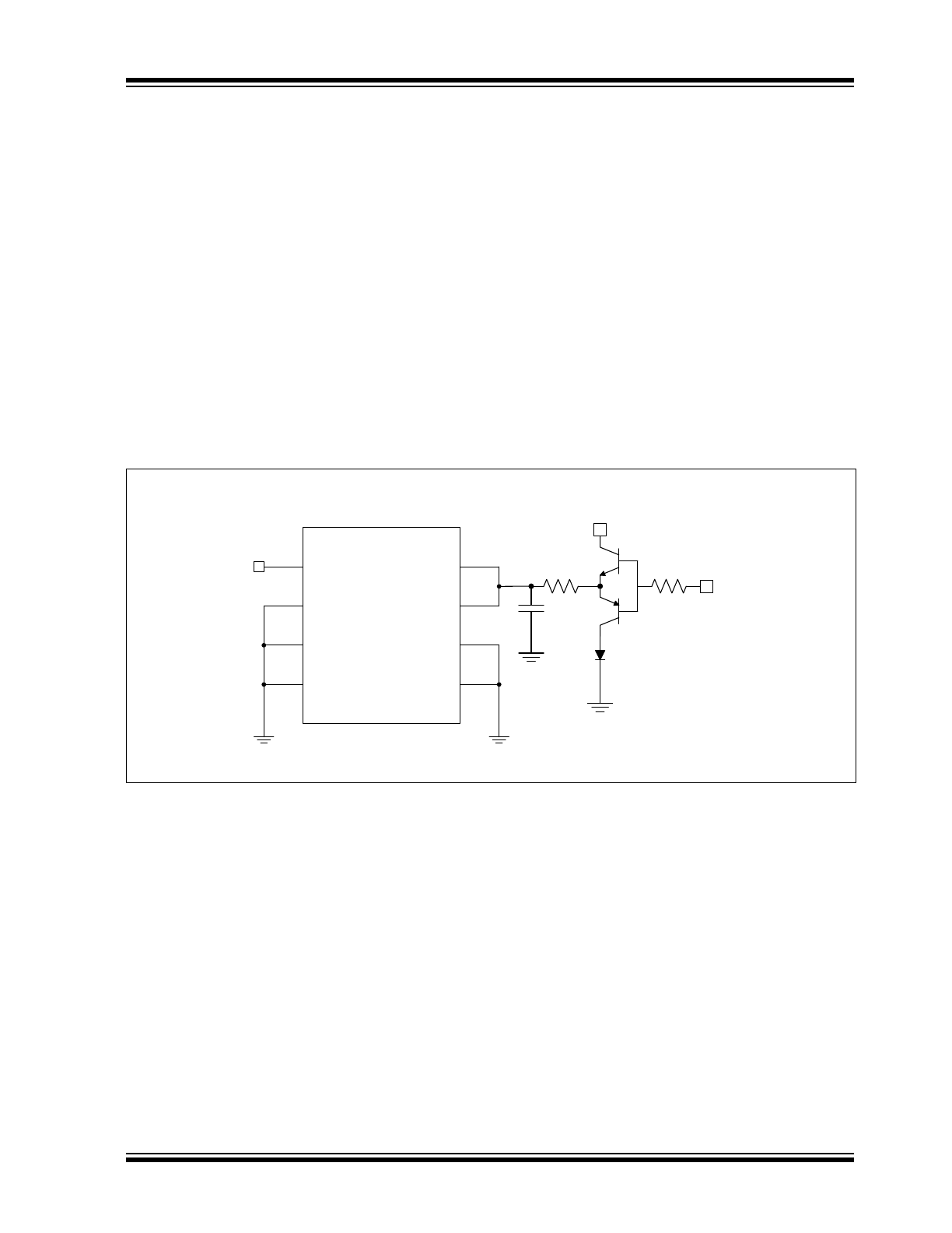
LONG-TERM DRIFT
The long-term output stability is measured by exposing
the devices to an ambient temperature of +125°C, as
shown in
Figure 2-18
while configured in the circuit
shown in
Figure 1-1
. In this test, all electrical specifica-
tions of the devices are measured periodically at
+25°C.
FIGURE 1-1:
Long-Term Drift Test Circuit.
1.1.10
OUTPUT VOLTAGE HYSTERESIS
The output voltage hysteresis is a measure of the out-
put voltage error after the powered devices are cycled
over the entire operating temperature range. The
amount of hysteresis can be quantified by measuring
the change in the +25°C output voltage after tempera-
ture excursions from +25°C to +125°C to +25°C, and
also from +25°C to –40°C to +25°C.
V
IN
GND
GND
GND
GND
GND
FB
V
OUT
Power
Signal In
MCP1501
DS20005474E-page 8
2015-2017 Microchip Technology Inc.
2.0
TYPICAL OPERATING CURVES
Note:
Unless otherwise specified, maximum values are: V
DD(MIN)
V
DD
5.5V at –40C T
A
+125C.
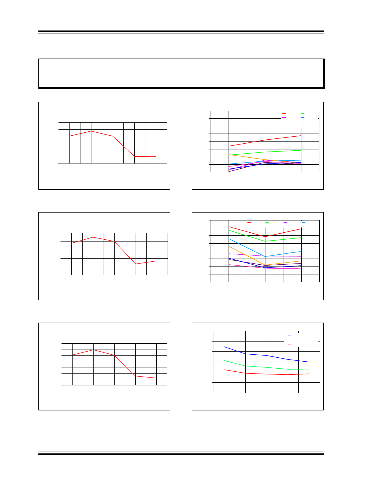
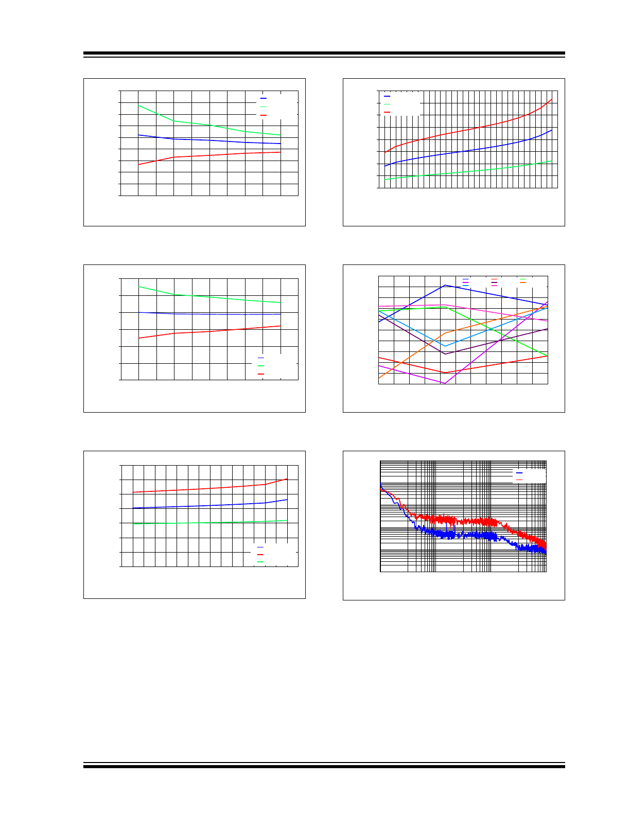
FIGURE 2-1:
V
OUT
vs. Temperature, No
Load, 4.096V Option.
FIGURE 2-2:
V
OUT
vs. Temperature, No
Load, 2.048V Option.
FIGURE 2-3:
V
OUT
vs. Temperature, No
Load, 1.024V Option.
FIGURE 2-4:
Load Regulation vs.
Temperature, I
LOAD
5mA Sink.
FIGURE 2-5:
Load Regulation vs.
Temperature, I
LOAD
5mA Source.
FIGURE 2-6:
I
DD
vs. Temperature, All
Options.
Note:
The graphs and tables provided following this note are a statistical summary based on a limited number of
samples and are provided for informational purposes only. The performance characteristics listed herein
are not tested or guaranteed. In some graphs or tables, the data presented may be outside the specified
operating range (e.g., outside specified power supply range) and therefore outside the warranted range.
4.092
4.093
4.094
4.095
4.096
4.097
4.098
-40
5
25
85
125
V
out (V)
Temperature (
°C)
2.046
2.0465
2.047
2.0475
2.048
2.0485
-40
5
25
85
125
V
out (V)
Temperature (
°C)
1.023
1.0232
1.0234
1.0236
1.0238
1.024
1.0242
1.0244
-40
5
25
85
125
V
out (V)
Temperature (
°C)
0
5
10
15
20
25
30
35
40
-40
25
125
Load Reg
(ppm/mA)
Temperature (
°C)
1.024V
1.25V
1.8V
2.048V
2.5V
3V
3.3V
4.096V
0
5
10
15
20
25
30
35
40
-40
25
125
Load Reg (ppm/mA)
Temperature (
°C)
1.024V
1.25V
1.8V
2.048V
2.5V
3V
3.3V
4.096V
150
175
200
225
250
275
300
-40
5
25
85
125
I
DD
(µA)
Temperature (
°C)
V
287
= 4.096V
V
287
= 2.048V
V
287
= 1.024V
2015-2017 Microchip Technology Inc.
DS20005474E-page 9
MCP1501
FIGURE 2-7:
I
DD
vs. Temperature for
V
OUT
, 50 Units, No Load, 4.096V Option.
FIGURE 2-8:
I
DD
vs. Temperature for
V
OUT
, 50 Units, No Load, 1.024V Option.
FIGURE 2-9:
I
DD
vs. V
DD
, V
OUT
= 4.096V,
50 Units, No Load.
FIGURE 2-10:
I
DD
vs. V
DD
, V
OUT
= 1.024V,
50 Units, No Load.
FIGURE 2-11:
Line Regulation vs.
Temperature.
FIGURE 2-12:
Noise vs. Frequency, No
Load, T
A
= +25°C.
0
50
100
150
200
250
300
350
400
450
-40
5
25
85
125
I
DD
(µA)
Temperature (
°C)
Average
+3 Sigma
-3 Sigma
0
50
100
150
200
250
300
-40
5
25
85
125
I
DD
(µA)
Temperature (
°C)
Average
+3 Sigma
-3 Sigma
0
50
100
150
200
250
300
350
4.3
4.45
4.6
4.75
4.9
5.05
5.2
5.5
I
DD
(µA)
V
DD
(V)
Average
+3 Sigma
-3 Sigma
100
120
140
160
180
200
220
240
260
1.65
2
2.25
2.5
2.75
3
3.25
3.5
3.75
4
4.25
4.5
4.75
5
5.25
5.5
I
DD
(µA)
V
DD
(V)
Average
-3 Sigma
+3 Sigma
0
0.5
1
1.5
2
2.5
3
3.5
4
4.5
5
-40 -25 -10
5
20
35
50
65
80
95 110 125
Line Reg (ppm/V)
Temperature (
°C)
V
287
= 1.8V
V
287
= 3.0V
V
287
= 1.024V
V
287
= 2.048V
V
287
= 3.3V
V
287
= 1.25V
V
287
= 2.5V
V
287
= 4.096V
0.01
0.1
1
10
100
1000
0.1
10
1000
100000
Noise Density
(uV/rtHz)
Frequency (Hz)
1.024V
4.096V
MCP1501
DS20005474E-page 10
2015-2017 Microchip Technology Inc.
FIGURE 2-13:
PSRR vs. Frequency, No
Load, T
A
= +25°C.
FIGURE 2-14:
PSRR vs. Frequency, 1 kΩ
Load, T
A
= +25°C.
FIGURE 2-15:
Dropout Voltage vs. Load,
T
A
= +25°C, 2.048V Option.
FIGURE 2-16:
Tempco Distribution, No
Load, T
A
= +25°C, V
DD
= 2.7V, 50 Units.
FIGURE 2-17:
Tempco Distribution, No
Load, T
A
= +25°C, V
DD
= 5.5V, 50 Units.
FIGURE 2-18:
V
OUT
Drift vs. Time,
T
A
= +25°C, No Load, 800 Units.
0
20
40
60
80
100
120
1
10
100
1000
10000
100000
PSRR (dB)
Frequency (Hz)
V
287
= 1.024, V
,1
= 1.65V
V
287
= 1.024V, V
,1
= 5.5V
V
287
= 4.096V, V
,1
= 4.3V
V
287
= 4.096V, V
,1
= 5.5V
0
20
40
60
80
100
120
1
10
100
1000
10000
100000
PSRR (dB)
Frequency (Hz)
V
287
= 1.024V, V
,1
= 1.65V
V
287
= 1.024V, V
,1
= 5.5V
V
287
= 4.096V, V
,1
= 4.3V
V
287
= 4.096V, V
,1
= 5.5V
0
20
40
60
80
100
120
140
160
-5
-2
0
2
5
Dropout V
oltage (mV)
Load (mA)
0
0.02
0.04
0.06
0.08
0.1
0.12
0.14
0.16
0.18
1
3
5
7
9 11 13 15 17 19 21 23 25 27 29
Percentage of
T
otal Units
Temperature Coefficient (ppm/
&)
0
0.02
0.04
0.06
0.08
0.1
0.12
0.14
0.16
1
3
5
7
9 11 13 15 17 19 21 23 25 27 29
Percentage of
T
otal
Units
Temperature Coefficient (ppm/
&)
-0.6
-0.4
-0.2
0
0.2
0.4
0.6
0.8
1
1.2
0
48
1008
V
OUT
Drift
(mV)
Time (Hrs)
Average
+3 Sigma
-3 Sigma