
2018 Microchip Technology Inc.
DS20005985A-page 1
MCP14A0453/4/5
Features
• High Peak Output Current: 4.5A (typical)
• Wide Input Supply Voltage Operating Range:
- 4.5V to 18V
• Low Shoot-Through/Cross-Conduction Current in
Output Stage
• High Capacitive Load Drive Capability:
- 2200 pF in 12 ns (typical)
• Short Delay Times: 16 ns (t
D1
), 19 ns (t
D2
) (typical)
• Low Supply Current: 620 µA (typical)
• Low-Voltage Threshold Input and Enable with
Hysteresis
• Latch-Up Protected: Withstands 500 mA Reverse
Current
• Space-Saving Packages:
- 8-Lead MSOP
- 8-Lead SOIC
- 8-Lead 2 x 3 TDFN
Applications
• Switch Mode Power Supplies
• Pulse Transformer Drive
• Line Drivers
• Level Translator
• Motor and Solenoid Drive
General Description
The MCP14A0453/4/5 devices are high-speed dual
MOSFET drivers that are capable of providing up to
4.5A of peak current while operating from a single 4.5V
to 18V supply. There are three output configurations
available: dual inverting (MCP14A0453), dual
noninverting (MCP14A0454) and complementary
(MCP14A0455). These devices feature low
shoot-through current, matched rise and fall times, and
short propagation delays, which make them ideal for
high switching frequency applications.
The MCP14A0453/4/5 family of devices offers
enhanced control with Enable functionality. The
active-high Enable pins can be driven low to drive the
corresponding outputs of the MCP14A0453/4/5 low,
regardless of the status of the Input pins. Integrated
pull-up resistors allow the user to leave the Enable pins
floating for standard operation.
These devices are highly latch-up resistant under any
condition within their power and voltage ratings. They
can accept up to 500 mA of reverse current being
forced back into their outputs without damage or logic
upset. All terminals are fully protected against
electrostatic discharge (ESD) up to 2 kV (HBM) and
200V (MM).
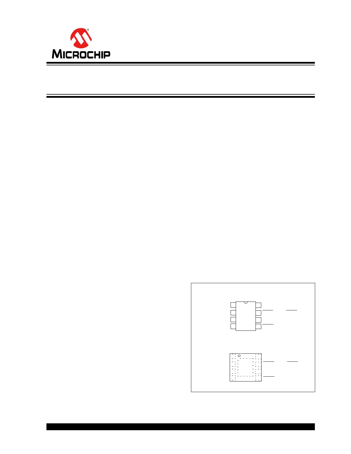
Package Types
* Includes Exposed Thermal Pad (EP); see
Table 3-1
.
MCP14A0453/4/5
MSOP/SOIC
GND
INA
INB
OUTA/OUTA/OUTA
V
DD
1
2
3
4
8
7
6
5 OUTB/OUTB/OUTB
ENB
ENA
GND
INA
INB
OUTA/OUTA/OUTA
V
DD
OUTB/OUTB/OUTB
ENB
ENA
MCP14A0453/4/5
2 x 3 TDFN*
1
2
3
4
8
7
6
5
EP*
9
4.5A Dual MOSFET Driver
with Low Threshold Input and Enable
MCP14A0453/4/5
DS20005985A-page 2
2018 Microchip Technology Inc.
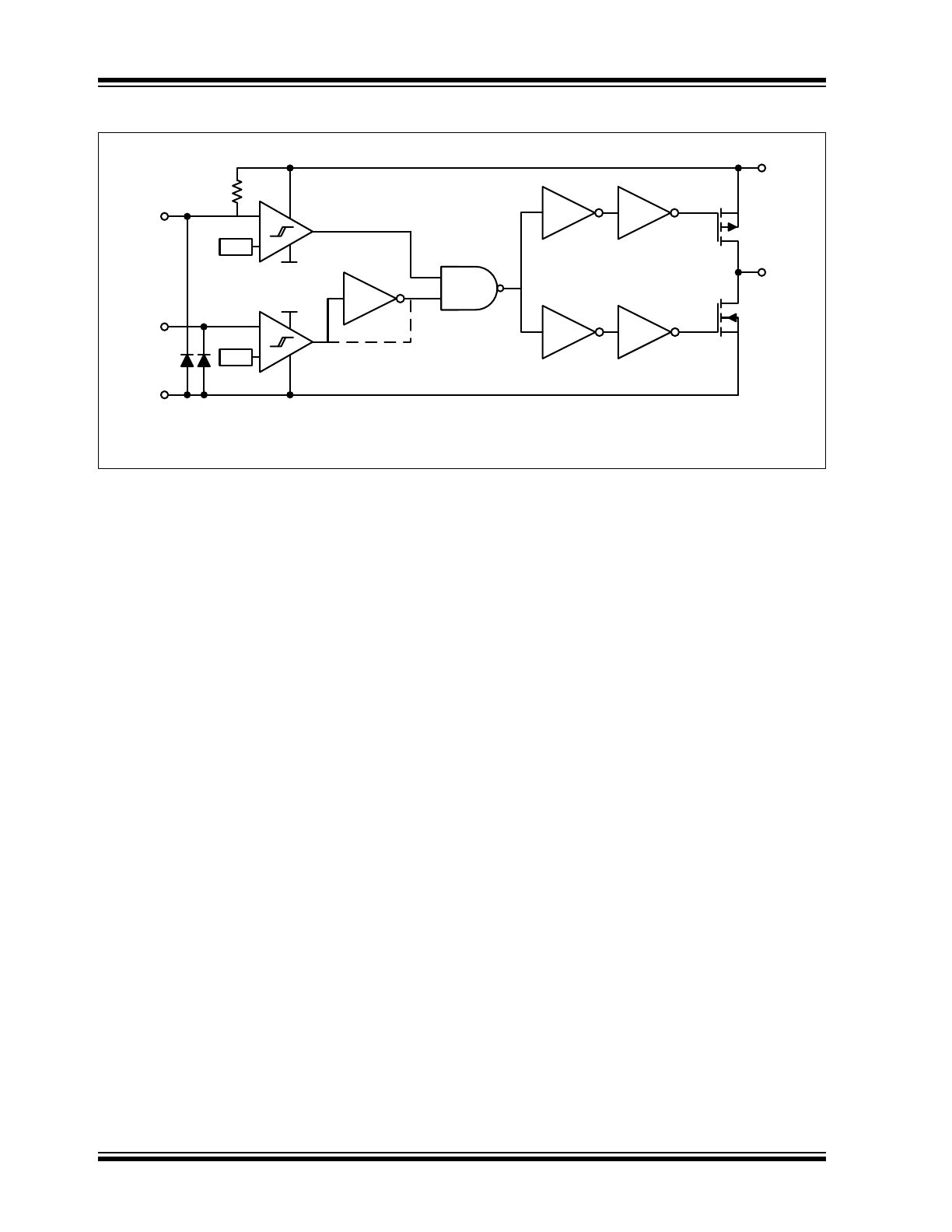
Functional Block Diagram
Non-Inverting
Enable
Input
V
DD
Output
Inverting
V
REF
V
REF
V
DD
GND
Internal
Pull-Up
MCP14A0453 Dual Invert ing
MCP14A0454 Dual Non-Inverting
MCP14A0455 Complementary: One I nverting, One Non-Inverting
GND

2018 Microchip Technology Inc.
DS20005985A-page 3
MCP14A0453/4/5
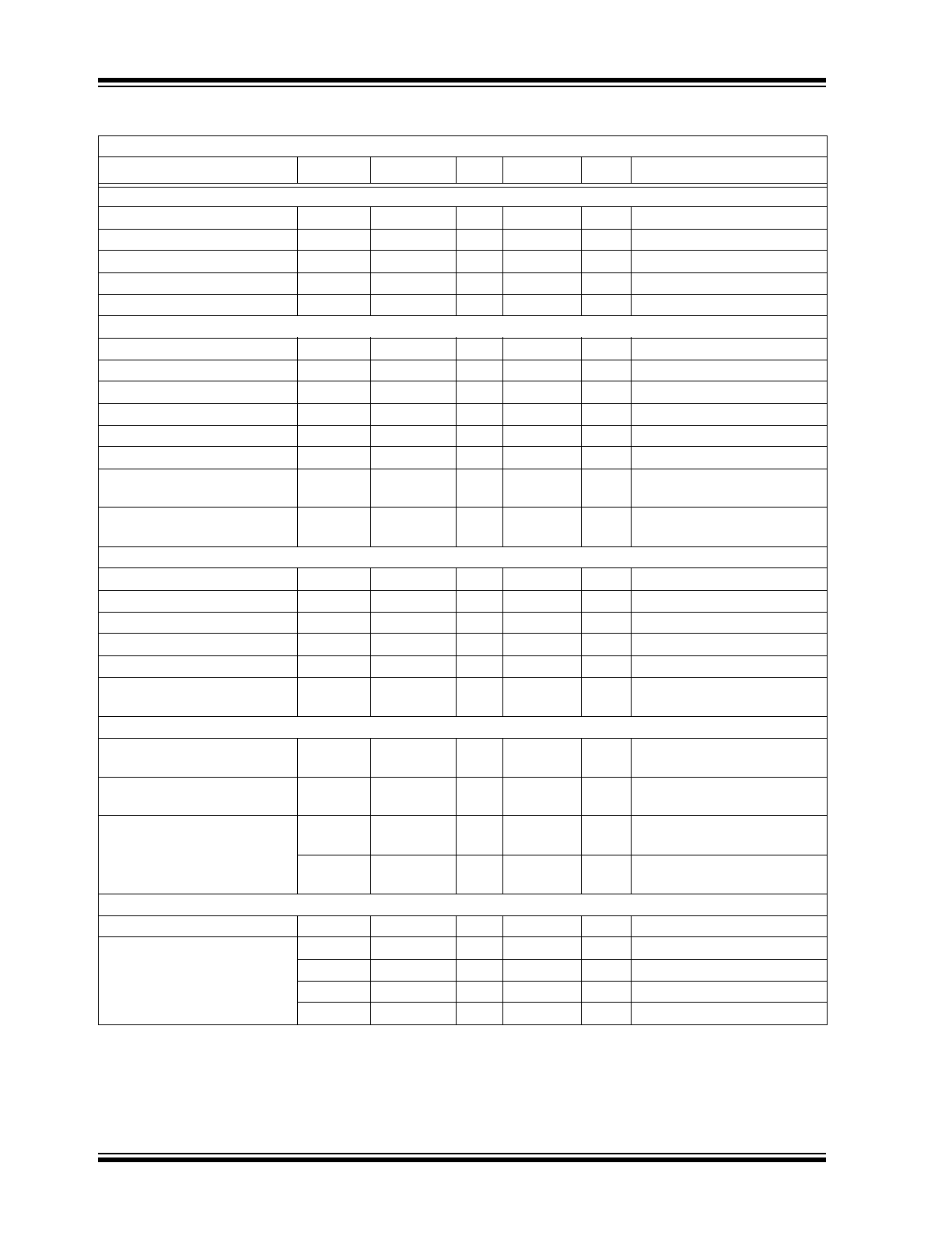
1.0
ELECTRICAL CHARACTERISTICS
1.1
Electrical Specifications
Absolute Maximum Ratings †
V
DD
, Supply Voltage..................................................................................................................................................+20V
V
IN
, Input Voltage............................................................................................................... (V
DD
+ 0.3V) to (GND – 0.3V)
V
EN
, Enable Voltage........................................................................................................... (V
DD
+ 0.3V) to (GND – 0.3V)
Package Power Dissipation (T
A
= +50°C)
8L MSOP .................................................................................................................................................0.63W
8L SOIC ...................................................................................................................................................1.00W
8L 2 X 3 TDFN .........................................................................................................................................1.85W
ESD protection on all pins ..............................................................................................................................2 kV (HBM)
ESD protection on all pins .............................................................................................................................. 200V (MM)
† Notice:
Stresses above those listed under “Maximum ratings” may cause permanent damage to the device. This is
a stress rating only and functional operation of the device at those or any other conditions above those indicated in
the operational listings of this specification is not implied. Exposure to maximum rating conditions for extended periods
may affect device reliability.
MCP14A0453/4/5
DS20005985A-page 4
2018 Microchip Technology Inc.
TABLE 1-1:
DC CHARACTERISTICS
Electrical Specifications:
Unless otherwise noted, T
A
= +25°C, with 4.5V
V
DD
18V.
Parameters
Sym.
Min.
Typ.
Max.
Units
Conditions
Input
Input Voltage Range
V
IN
GND – 0.3V
—
V
DD
+ 0.3
V
Logic ‘1’ High Input Voltage
V
IH
2.0
1.6
—
V
Logic ‘0’ Low Input Voltage
V
IL
—
1.3
0.8
V
Input Voltage Hysteresis
V
HYST(IN)
—
0.3
—
V
Input Current
I
IN
–1
—
+1
µA
0V
V
IN
V
DD
Enable
Enable Voltage Range
V
EN
GND – 0.3V
—
V
DD
+ 0.3
V
Logic ‘1’ High Enable Voltage
V
EH
2.0
1.6
—
V
Logic ‘0’ Low Enable Voltage
V
EL
—
1.3
0.8
V
Enable Voltage Hysteresis
V
HYST(EN)
—
0.3
—
V
Enable Pin Pull-Up Resistance
R
ENBL
—
1.5
—
MΩ
V
DD
= 18V, ENB = A
GND
Enable Input Current
I
EN
—
12
—
µA
V
DD
= 18V, ENB = A
GND
Propagation Delay
t
D3
—
16
23
ns
V
DD
= 18V, V
EN
= 5V,
see
Figure 4-3
, (
Note 1
)
Propagation Delay
t
D4
—
19
26
ns
V
DD
= 18V, V
EN
= 5V,
see
Figure 4-3
, (
Note 1
)
Output
High Output Voltage
V
OH
V
DD
– 0.025
—
—
V
I
OUT
= 0A
Low Output Voltage
V
OL
—
—
0.025
V
I
OUT
= 0A
Output Resistance, High
R
OH
—
1.7
2.7
Ω
I
OUT
= 10 mA, V
DD
= 18V
Output Resistance, Low
R
OL
—
1.3
2.3
Ω
I
OUT
= 10 mA, V
DD
= 18V
Peak Output Current
I
PK
—
4.5
—
A
V
DD
= 18V (
Note 1
)
Latch-Up Protection Withstand
Reverse Current
I
REV
0.5
—
—
A
Duty cycle
2%, t 300 µs
(
Note 1
)
Switching Time (
Note 1
)
Rise Time
t
R
—
12
17
ns
V
DD
= 18V, C
L
= 1800 pF,
see
Figure 4-1
,
Figure 4-2
Fall Time
t
F
—
12
17
ns
V
DD
= 18V, C
L
= 1800 pF,
see
Figure 4-1
,
Figure 4-2
Delay Time
t
D1
—
16
23
ns
V
DD
= 18V, V
IN
= 5V,
see
Figure 4-1
,
Figure 4-2
t
D2
—
19
26
ns
V
DD
= 18V, V
IN
= 5V,
see
Figure 4-1
,
Figure 4-2
Power Supply
Supply Voltage
V
DD
4.5
—
18
V
Power Supply Current
I
DD
—
620
900
µA
V
INA/B
= 3V, V
ENA/B
= 3V
I
DD
—
620
900
µA
V
INA/B
= 0V, V
ENA/B
= 3V
I
DD
—
620
900
µA
V
INA/B
= 3V, V
ENA/B
= 0V
I
DD
—
620
900
µA
V
INA/B
= 0V, V
ENA/B
= 0V
Note 1:
Tested during characterization, not production tested.
2018 Microchip Technology Inc.
DS20005985A-page 5
MCP14A0453/4/5
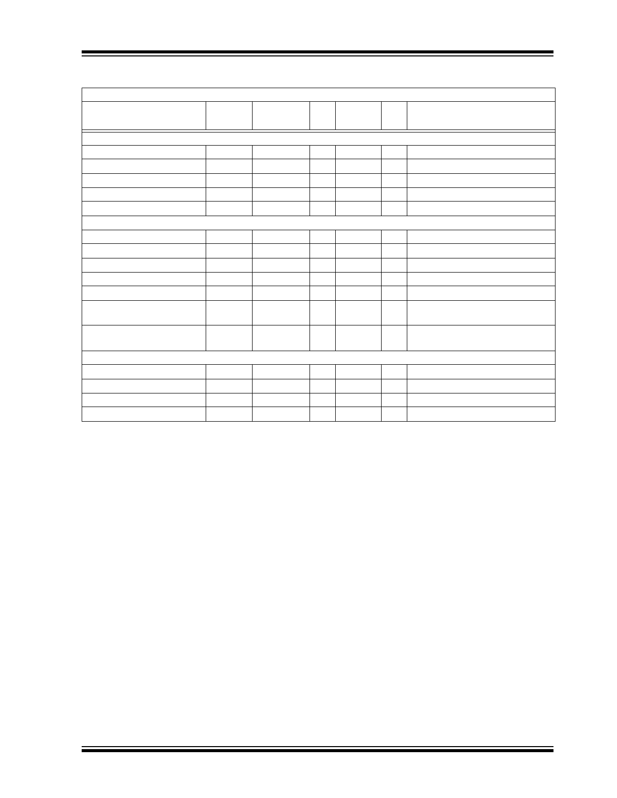
TABLE 1-2:
DC CHARACTERISTICS (OVER OPERATING TEMP. RANGE)
Electrical Specifications:
Unless otherwise indicated, over the operating range with 4.5V
V
DD
18V.
Parameters
Sym.
Min.
Typ.
Max.
Unit
s
Conditions
Input
Input Voltage Range
V
IN
GND – 0.3V
—
V
DD
+ 0.3
V
Logic ‘1’ High Input Voltage
V
IH
2.0
1.6
—
V
Logic ‘0’ Low Input Voltage
V
IL
—
1.3
0.8
V
Input Voltage Hysteresis
V
HYST(IN)
—
0.3
—
V
Input Current
I
IN
–10
—
+10
µA
0V
V
IN
V
DD
Enable
Enable Voltage Range
V
EN
GND – 0.3V
—
V
DD
+ 0.3
V
Logic ‘1’ High Enable Voltage
V
EH
2.0
1.6
—
V
Logic ‘0’ Low Enable Voltage
V
EL
—
1.3
0.8
V
Enable Voltage Hysteresis
V
HYST(EN)
—
0.3
—
V
Enable Input Current
I
EN
—
12
—
µA
V
DD
= 18V, ENB = A
GND
Propagation Delay
t
D3
—
20
27
ns
V
DD
= 18V, V
EN
= 5V, T
A
= +125°C,
see
Figure 4-3
, (
Note 1
)
Propagation Delay
t
D4
—
24
31
ns
V
DD
= 18V, V
EN
= 5V, T
A
= +125°C,
see
Figure 4-3
, (
Note 1
)
Output
High Output Voltage
V
OH
V
DD
– 0.025
—
—
V
DC Test
Low Output Voltage
V
OL
—
—
0.025
V
DC Test
Output Resistance, High
R
OH
—
—
3.3
Ω
I
OUT
= 10 mA, V
DD
= 18V
Output Resistance, Low
R
OL
—
—
2.9
Ω
I
OUT
= 10 mA, V
DD
= 18V
Note 1:
Tested during characterization, not production tested.
MCP14A0453/4/5
DS20005985A-page 6
2018 Microchip Technology Inc.
Switching Time (
Note 1
)
Rise Time
t
R
—
14
19
ns
V
DD
= 18V, C
L
= 1800 pF,
T
A
= +125°C, see
Figure 4-1
,
Figure 4-2
Fall Time
t
F
—
14
19
ns
V
DD
= 18V, C
L
= 1800 pF,
T
A
= +125°C, see
Figure 4-1
,
Figure 4-2
Delay Time
t
D1
—
20
27
ns
V
DD
= 18V, V
IN
= 5V, T
A
= +125°C,
see
Figure 4-1
,
Figure 4-2
t
D2
—
24
31
V
DD
= 18V, V
IN
= 5V, T
A
= +125°C,
see
Figure 4-1
,
Figure 4-2
Power Supply
Supply Voltage
V
DD
4.5
—
18
V
Power Supply Current
I
DD
—
—
1100
µA
V
INA/B
= 3V, V
ENA/B
= 3V
I
DD
—
—
1100
µA
V
INA/B
= 0V, V
ENA/B
= 3V
I
DD
—
—
1100
µA
V
INA/B
= 3V, V
ENA/B
= 0V
I
DD
—
—
1100
µA
V
INA/B
= 0V, V
ENA/B
= 0V
1.2
Temperature Characteristics
Electrical Specifications:
Unless otherwise noted, all parameters apply with 4.5V
V
DD
18V
Parameter
Sym.
Min.
Typ.
Max.
Units
Comments
Temperature Ranges
Specified Temperature Range
T
A
-40
—
+125
°C
Maximum Junction Temperature
T
J
—
—
+150
°C
Storage Temperature Range
T
A
-65
—
+150
°C
Package Thermal Resistances
Junction-to-Ambient Thermal Resistance, 8LD MSOP
JA
—
158
—
°C/W
Note 1
Junction-to-Ambient Thermal Resistance, 8LD SOIC
JA
—
100
—
°C/W
Note 1
Junction-to-Ambient Thermal Resistance, 8LD TDFN
JA
—
54
—
°C/W
Note 1
Junction-to-Top Characterization Parameter, 8LD MSOP
JT
—
2.4
—
°C/W
Note 1
Junction-to-Top Characterization Parameter, 8LD SOIC
JT
—
5.9
—
°C/W
Note 1
Junction-to-Top Characterization Parameter, 8LD TDFN
JT
—
0.5
—
°C/W
Note 1
Junction-to-Board Characterization Parameter, 8LD MSOP
JB
—
115
—
°C/W
Note 1
Junction-to-Board Characterization Parameter, 8LD SOIC
JB
—
65
—
°C/W
Note 1
Junction-to-Board Characterization Parameter, 8LD TDFN
JB
—
24
—
°C/W
Note 1
Note 1:
Parameter is determined using High K 2S2P 4-Layer board as described in JESD 51-7, as well as JESD
51-5 for packages with exposed pads.
TABLE 1-2:
DC CHARACTERISTICS (OVER OPERATING TEMP. RANGE) (CONTINUED)
Electrical Specifications:
Unless otherwise indicated, over the operating range with 4.5V
V
DD
18V.
Parameters
Sym.
Min.
Typ.
Max.
Unit
s
Conditions
Note 1:
Tested during characterization, not production tested.
2018 Microchip Technology Inc.
DS20005985A-page 7
MCP14A0453/4/5
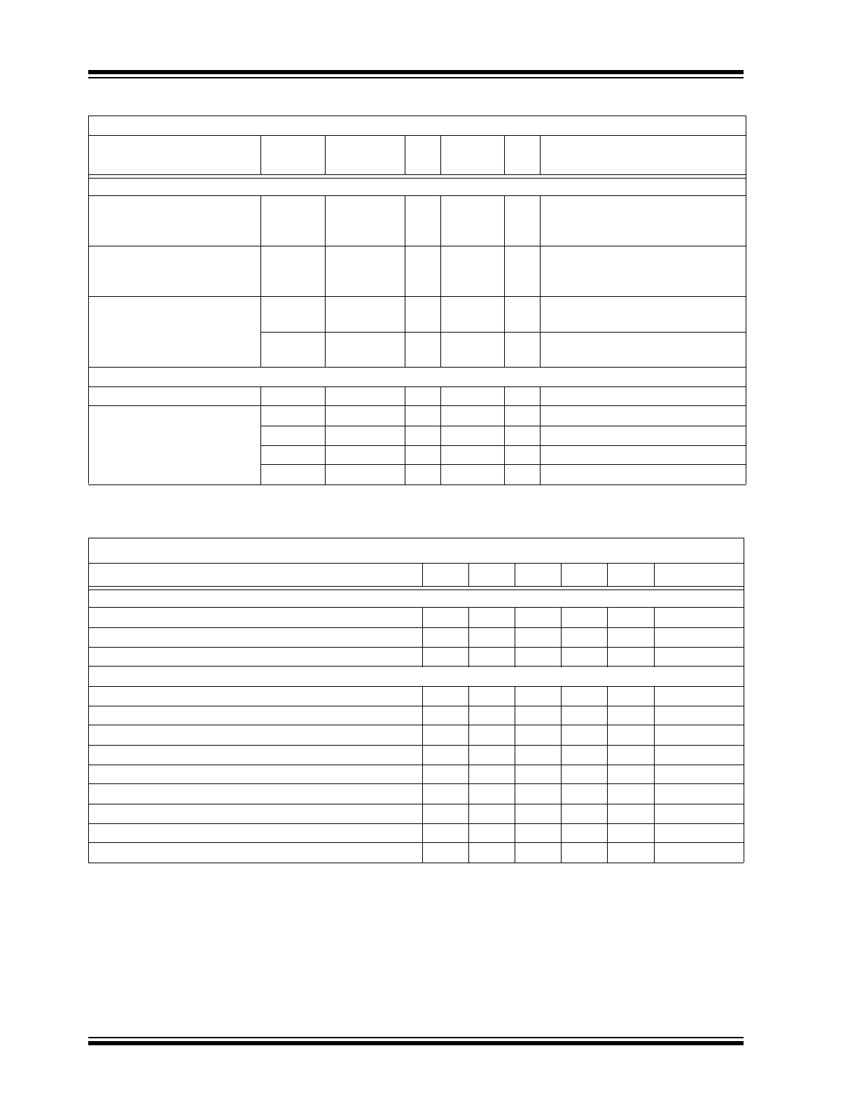
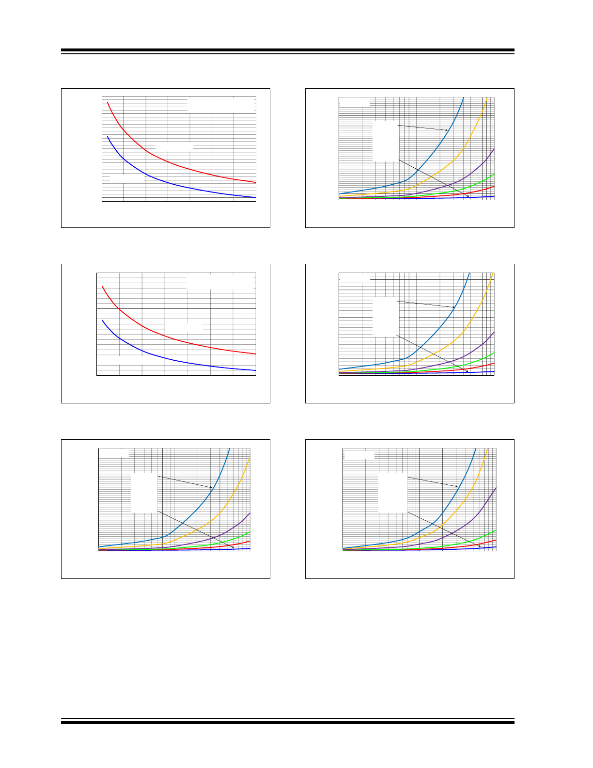
2.0
TYPICAL PERFORMANCE CURVES
Note:
Unless otherwise indicated, T
A
= +25°C with 4.5V
V
DD
18V.
FIGURE 2-1:
Rise Time vs. Supply
Voltage.
FIGURE 2-2:
Rise Time vs. Capacitive
Load.
FIGURE 2-3:
Fall Time vs. Supply
Voltage.
FIGURE 2-4:
Fall Time vs. Capacitive
Load.
FIGURE 2-5:
Rise and Fall Time vs.
Temperature.
FIGURE 2-6:
Crossover Current vs.
Supply Voltage.
Note:
The graphs and tables provided following this note are a statistical summary based on a limited number of
samples and are provided for informational purposes only. The performance characteristics listed herein
are not tested or guaranteed. In some graphs or tables, the data presented may be outside the specified
operating range (e.g., outside specified power supply range) and therefore outside the warranted range.
0
20
40
60
80
100
120
4
6
8
10
12
14
16
18
Rise T
ime (n
s)
Supply Voltage (V)
10000 pF
6800 pF
4700 pF
3300 pF
2200 pF
1000 pF
0
20
40
60
80
100
120
1000
10000
Rise T
ime (ns)
Capacitive Load (pF)
18V
12V
5V
0
10
20
30
40
50
60
70
80
4
6
8
10
12
14
16
18
Fall T
ime (ns)
Supply Voltage (V)
10000 pF
6800 pF
4700 pF
3300 pF
2200 pF
1000 pF
0
10
20
30
40
50
60
70
80
1000
10000
Fall T
ime
(ns)
Capacitive Load (pF)
18V
12V
5V
8
10
12
14
16
18
20
22
24
26
-40 -25 -10
5
20
35
50
65
80
95 110 125
T
ime (ns)
Temperature (°C)
V
DD
= 18V
t
F
, 4700 pF
t
R
, 4700 pF
t
R
, 2200 pF
t
F
, 2200 pF
10
100
1000
10000
4
6
8
10
12
14
16
18
Crossover Current
(
µ
A)
Supply Voltage (V)
1 MHz
500 kHz
200 kHz
100 kHz
50 kHz
MCP14A0453/4/5
DS20005985A-page 8
2018 Microchip Technology Inc.
Note:
Unless otherwise indicated, T
A
= +25°C with 4.5V
V
DD
18V.
FIGURE 2-7:
Input Propagation Delay vs.
Supply Voltage.
FIGURE 2-8:
Input Propagation Delay
Time vs. Input Amplitude.
FIGURE 2-9:
Input Propagation Delay vs.
Temperature.
FIGURE 2-10:
Enable Propagation Delay
vs. Supply Voltage.
FIGURE 2-11:
Enable Propagation Delay
Time vs. Enable Voltage Amplitude.
FIGURE 2-12:
Enable Propagation Delay
vs. Temperature.
10
15
20
25
30
35
40
45
50
4
6
8
10
12
14
16
18
Input Propagation
Delay
(ns)
Supply Voltage (V)
V
IN
= 5V
t
D1
t
D2
10
15
20
25
2
4
6
8
10
12
14
16
18
Input Propogati
on Delay
(ns)
Input Voltage Amplitude (V)
t
D2
t
D1
V
DD
= 18V
12
14
16
18
20
22
24
26
-40 -25 -10
5
20
35
50
65
80
95 110 125
Input Propagation
Del
ay
(ns)
Temperature (°C)
V
DD
= 18V
t
D2
t
D1
V
IN
= 5V
10
15
20
25
30
35
40
45
50
4
6
8
10
12
14
16
18
Enable Propagation Delay
(ns)
Supply Voltage (V)
V
EN
= 5V
t
D3
t
D4
10
15
20
25
30
2
4
6
8
10
12
14
16
18
Enable Propagation Delay
(ns)
Enable Voltage Amplitude (V)
t
D4
t
D3
V
DD
= 18V
12
14
16
18
20
22
24
26
-40 -25 -10
5
20
35
50
65
80
95 110 125
Enabl
e
Propagation Del
ay
(ns)
Temperature (°C)
t
D4
t
D3
V
DD
= 18V
V
EN
= 5V
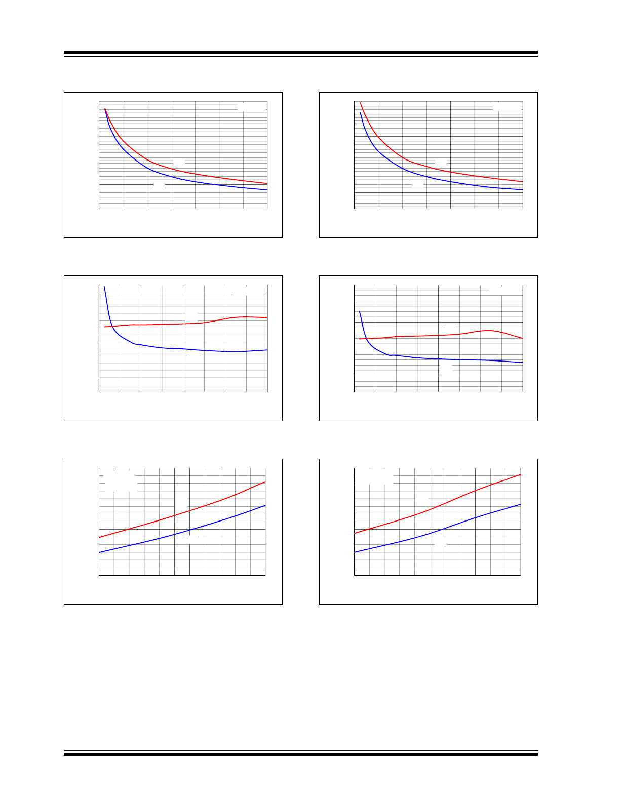
2018 Microchip Technology Inc.
DS20005985A-page 9
MCP14A0453/4/5
Note:
Unless otherwise indicated, T
A
= +25°C with 4.5V
V
DD
18V.
FIGURE 2-13:
Quiescent Supply Current
vs. Supply Voltage.
FIGURE 2-14:
Quiescent Supply Current
vs. Temperature.
FIGURE 2-15:
Input Threshold vs.
Temperature.
FIGURE 2-16:
Input Threshold vs. Supply
Voltage.
FIGURE 2-17:
Enable Threshold vs.
Temperature.
FIGURE 2-18:
Enable Threshold vs.
Supply Voltage.
550
600
650
4
6
8
10
12
14
16
18
Q
u
iescent
Current (
µ
A)
Supply Voltage (V)
500
550
600
650
700
750
800
-40 -25 -10
5
20
35
50
65
80
95 110 125
Qu
ie
sc
e
n
t C
u
rr
ent (µ
A)
Temperature (°C)
V
DD
= 18V
1
1.1
1.2
1.3
1.4
1.5
1.6
1.7
1.8
-40 -25 -10
5
20
35
50
65
80
95 110 125
Input Threshold
(V)
Temperature (°C)
V
DD
= 18V
V
IL
V
IH
1.0
1.1
1.2
1.3
1.4
1.5
1.6
1.7
1.8
4
6
8
10
12
14
16
18
Input Threshold
(V)
Supply Voltage (V)
V
IL
V
IH
1
1.1
1.2
1.3
1.4
1.5
1.6
1.7
1.8
-40 -25 -10
5
20
35
50
65
80
95 110 125
Enable Threshold (V)
Temperature (°C)
V
DD
= 18V
V
EL
V
EH
1
1.1
1.2
1.3
1.4
1.5
1.6
1.7
1.8
4
6
8
10
12
14
16
18
Enable Threshold (V)
Supply Voltage (V)
V
EL
V
EH
MCP14A0453/4/5
DS20005985A-page 10
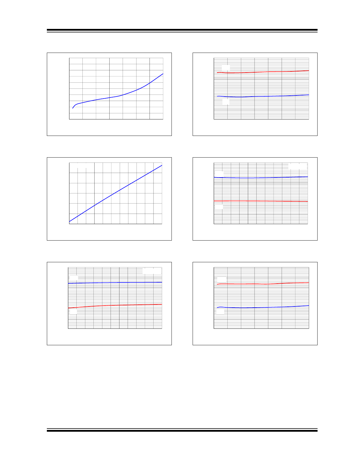
2018 Microchip Technology Inc.
Note:
Unless otherwise indicated, T
A
= +25°C with 4.5V
V
DD
18V.
FIGURE 2-19:
Output Resistance (Output
High) vs. Supply Voltage.
FIGURE 2-20:
Output Resistance (Output
Low) vs. Supply Voltage.
FIGURE 2-21:
Supply Current vs.
Capacitive Load (V
DD
= 18V).
FIGURE 2-22:
Supply Current vs.
Capacitive Load (V
DD
= 12V).
FIGURE 2-23:
Supply Current vs.
Capacitive Load (V
DD
= 6V).
FIGURE 2-24:
Supply Current vs.
Frequency (V
DD
= 18V).
1.5
2.0
2.5
3.0
3.5
4.0
4.5
4
6
8
10
12
14
16
18
R
OH
-
O
utput Resist
ance
(
)
Supply Voltage (V)
T
A
= +25°C
T
A
= +125°C
V
IN
= 0V (MCP14A0453)
V
IN
= 5V (MCP14A0454)
1
1.5
2
2.5
3
4
6
8
10
12
14
16
18
R
OL
-
O
ut
put
Resistance
(
)
Supply Voltage (V)
T
A
= +25°C
T
A
= +125°C
V
IN
= 5V (MCP14A0453)
V
IN
= 0V (MCP14A0454)
0
10
20
30
40
50
60
70
80
90
100
100
1000
10000
Supply
Current
(m
A)
Capacitive Load (pF)
1 MHz
500 kHz
200 kHz
100 kHz
50 kHz
10 kHz
V
DD
= 18V
0
5
10
15
20
25
30
35
40
45
50
100
1000
10000
Suppl
y
Current
(mA)
Capacitive Load (pF)
1 MHz
500 kHz
200 kHz
100 kHz
50 kHz
10 kHz
V
DD
= 12V
0
5
10
15
20
25
30
100
1000
10000
Supply
Current
(m
A)
Capacitive Load (pF)
1 MHz
500 kHz
200 kHz
100 kHz
50 kHz
10 kHz
V
DD
= 6V
0
10
20
30
40
50
60
70
80
90
100
10
100
1000
Suppl
y
Current
(mA)
Switching Frequency (kHz)
10000 pF
6800 pF
3300 pF
1000 pF
470 pF
100 pF
V
DD
= 18V