
2009-2013 Microchip Technology Inc.
DS22201B-page 1
MCP14700
Features:
• Ideally suited to drive low Figure-of-Merit (FOM)
MOSFETs such as Microchip’s MCP87000
MOSFET family
• Independent PWM Input Control for High-Side
and Low-Side Gate Drive
• Input Logic Level Threshold 3.0V TTL Compatible
• Dual Output MOSFET Drive for Synchronous
Applications
• High Peak Output Current: 2A (typical)
• Internal Bootstrap Blocking Device
• +36V BOOT Pin Maximum Rating
• Low Supply Current: 45 µA (typical)
• High Capacitive Load Drive Capability:
- 3300 pF in 10.0 ns (typical)
• Input Voltage Undervoltage Lockout Protection
• Overtemperature Protection
• Space Saving Packages:
- 8-Lead SOIC
- 8-Lead 3x3 DFN
Applications:
• 3-Phase BLDC Motor Control
• High Efficient Synchronous DC/DC Buck
Converters
• High-Current Low Output Voltage Synchronous
DC/DC Buck Converters
• High Input Voltage Synchronous DC/DC Buck
Converters
• Core Voltage Supplies for Microprocessors
General Description:
The MCP14700 is a high-speed synchronous
MOSFET driver designed to optimally drive a high-side
and low-side N-Channel MOSFET. It is particularly well
suited for driving low-FOM MOSFETs, including
Microchip’s MCP87000 family of high-speed
MOSFETs. The MCP14700 has two PWM inputs to
allow independent control of the external N-Channel
MOSFETs. Since there is no internal cross conduction
protection circuitry the external MOSFET dead time
can be tightly controlled allowing for more efficient
systems or unique motor control algorithms.
The transition thresholds for the PWM inputs are
typically 1.6V on a rising PWM input signal and typically
1.2V on a falling PWM input signal. This makes the
MCP14700 ideally suited for controllers that utilize 3.0V
TTL/CMOS logic. The PWM inputs are internally pulled
low ensuring the output drive signals are low if the
inputs are floating.
The HIGHDR and LOWDR peak source current
capability of the MCP14700 device is typically 2A.
While the HIGHDR can sink 2A peak typically, the
LOWDR can sink 3.5A peak typically. The low
resistance pull-up and pull-down drive allow the
MCP14700 to quickly transition a 3300 pF load in
typically 10 ns. Bootstrapping for the high-side drive is
internally implemented which allows for a reduced
system cost and design complexity.
The MCP14700 features undervoltage lockout (UVLO)
with a typical hysteresis of 500 mV. Overtemperature
protection with hysteresis is also featured on the
device.
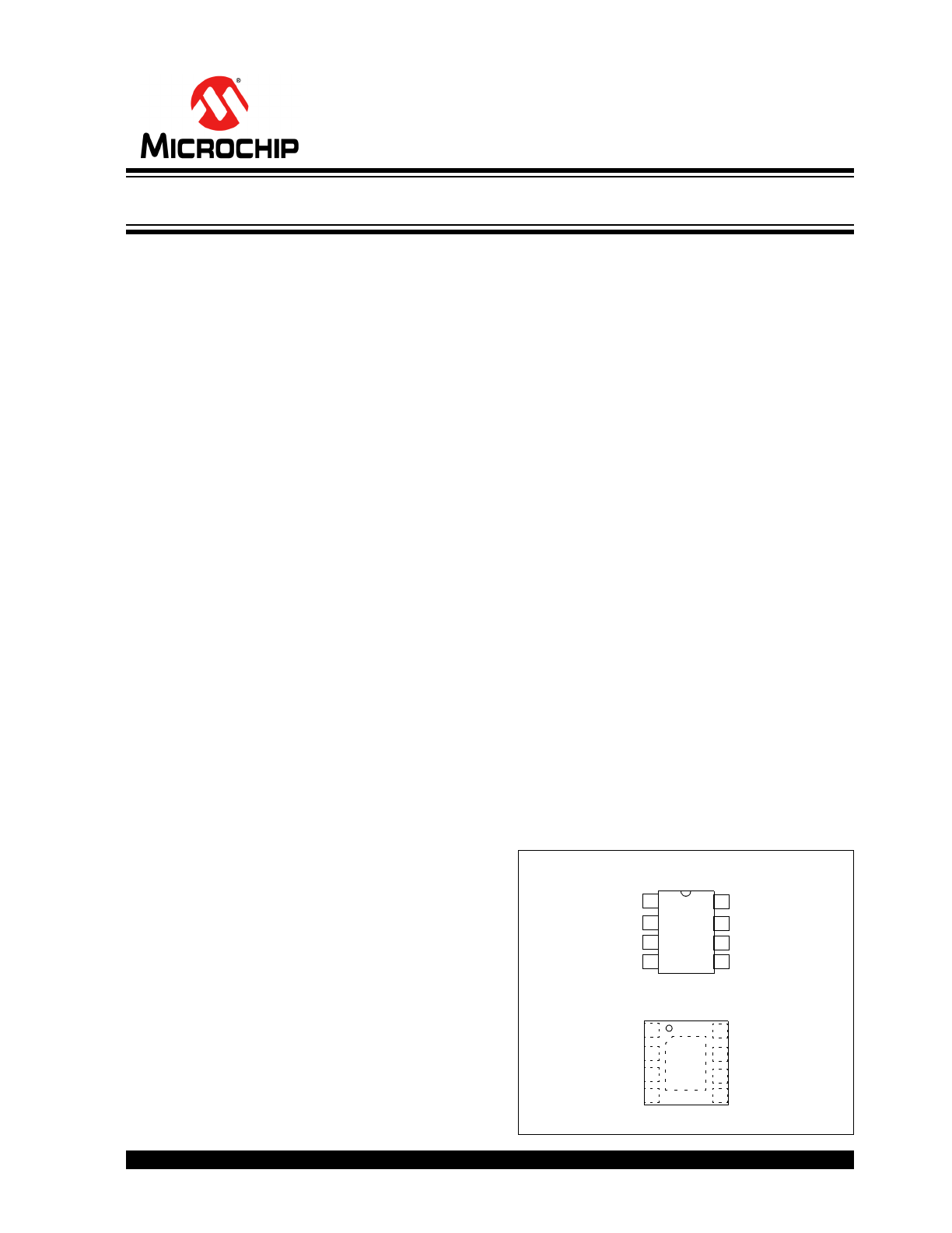
Package Types
MCP14700
3x3 DFN*
PWM
LO
PWM
HI
GND
BOOT
V
CC
1
2
3
4
8
7
6
5
LOWDR
HIGHDR
PHASE
* Includes Exposed Thermal Pad (EP); see
Table 3-1
.
EP
9
MCP14700
SOIC
PWM
LO
PWM
HI
GND
BOOT
V
CC
1
2
3
4
8
7
6
5
LOWDR
HIGHDR
PHASE
Dual Input Synchronous MOSFET Driver
MCP14700
DS22201B-page 2
2009-2013 Microchip Technology Inc.
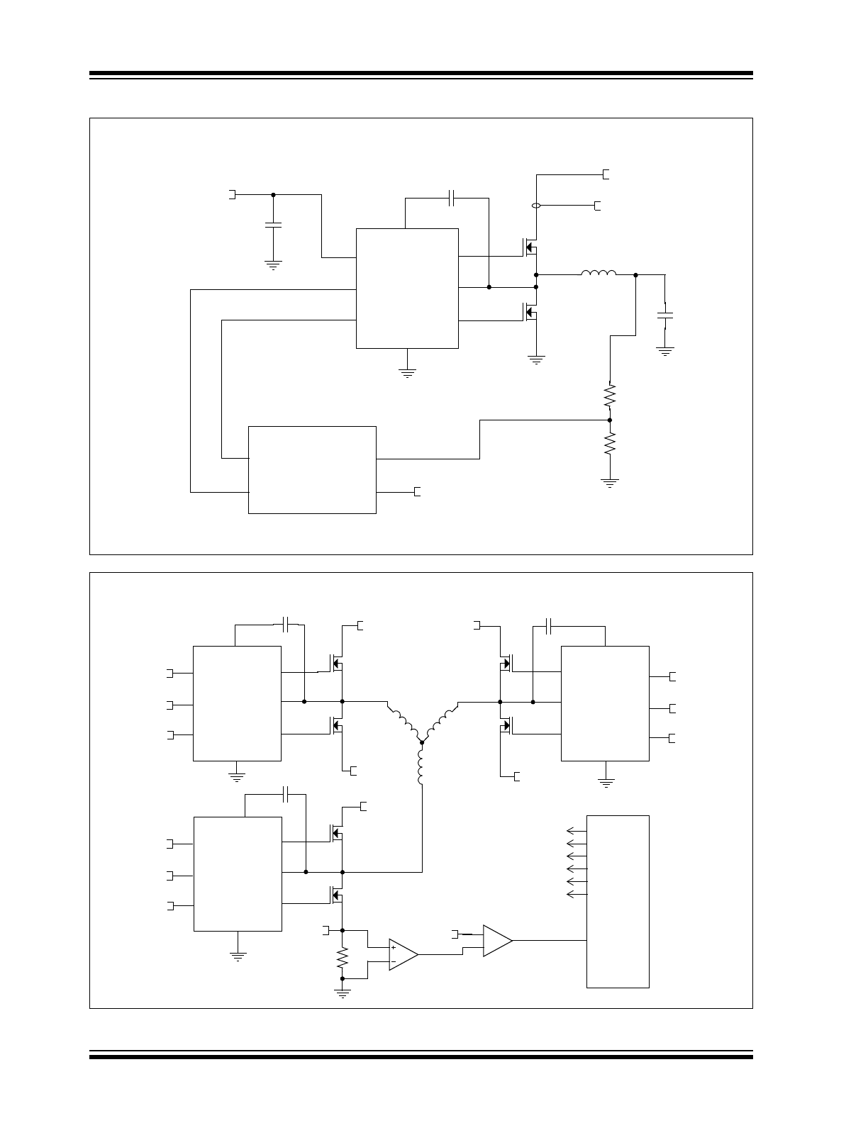
Typical Application Schematic
HIGHDR
LOWDR
PHASE
V
CC
PWM
LO
BOOT
GND
PWM
HI
V
BUCK
= 12V
V
CC
= 5.0V
C
BOOT
dsPIC33FJ06GS101
CURRENT
SENSE
CURRENT
SENSE
PWM1L
PWM1H
AN0
AN1
MCP14700
Synchronous Buck Application
MCP87050
MCP87022
HIGHDR
LOWDR
PHASE
V
CC
PWM
LO
BOOT
GND
PWM
HI
HIGHDR
LOWDR
PHASE
V
CC
PWM
LO
BOOT
GND
PWM
HI
HIGHDR
LOWDR
PHASE
V
CC
PWM
LO
BOOT
GND
PWM
H
PWM2
PWM1
V
CC
PWM4
PWM3
V
CC
PWM6
PWM5
V
CC
24V
24V
24V
SENSE
NODE
V
REF
PWM1
PWM2
PWM3
PWM4
PWM5
PWM6
dsPIC
®
MCP14700
MCP14700
SENSE
NODE
MCP14700
3-Phase BLDC Motor Control Application
SENSE
NODE
2009-2013 Microchip Technology Inc.
DS22201B-page 3
MCP14700
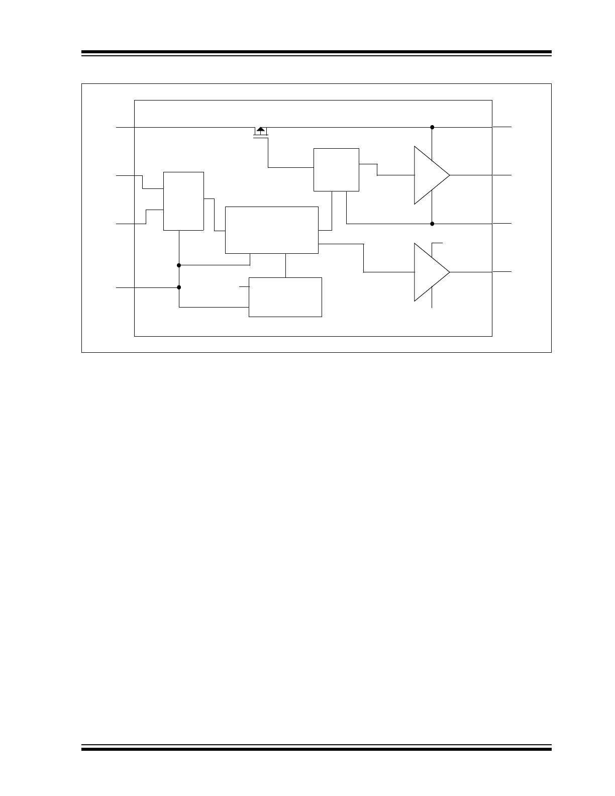
Functional Block Diagram
BOOT
HIGHDR
PHASE
LOWDR
V
CC
PWM
HI
PWM
LO
GND
Level
Shift
Input
Protection
Logic
V
CC
Circuitry
Circuitry
GND
V
CC

MCP14700
DS22201B-page 4
2009-2013 Microchip Technology Inc.
NOTES:
2009-2013 Microchip Technology Inc.
DS22201B-page 5
MCP14700
1.0
ELECTRICAL
CHARACTERISTICS
Absolute Maximum Ratings †
V
CC
........................................................ -0.3V to +7.0V
V
BOOT
.................................................. -0.3V to +36.0V
V
PHASE
............................ V
BOOT
- 7V to V
BOOT
+ 0.3V
V
PWM
.............................................-0.3V to V
CC
+ 0.3V
V
HIGHDR
......................V
PHASE
- 0.3V to V
BOOT
+ 0.3V
V
LOWDR
.........................................-0.3V to V
CC
+ 0.3V
ESD Protection on all Pins .........................2 kV (HBM)
....................................................................400V (MM)
† Notice: Stresses above those listed under “Maximum
Ratings” may cause permanent damage to the device.
This is a stress rating only and functional operation of
the device at those or any other conditions above those
indicated in the operational sections of this specifica-
tion is not intended. Exposure to maximum rating con-
ditions for extended periods may affect device
reliability.
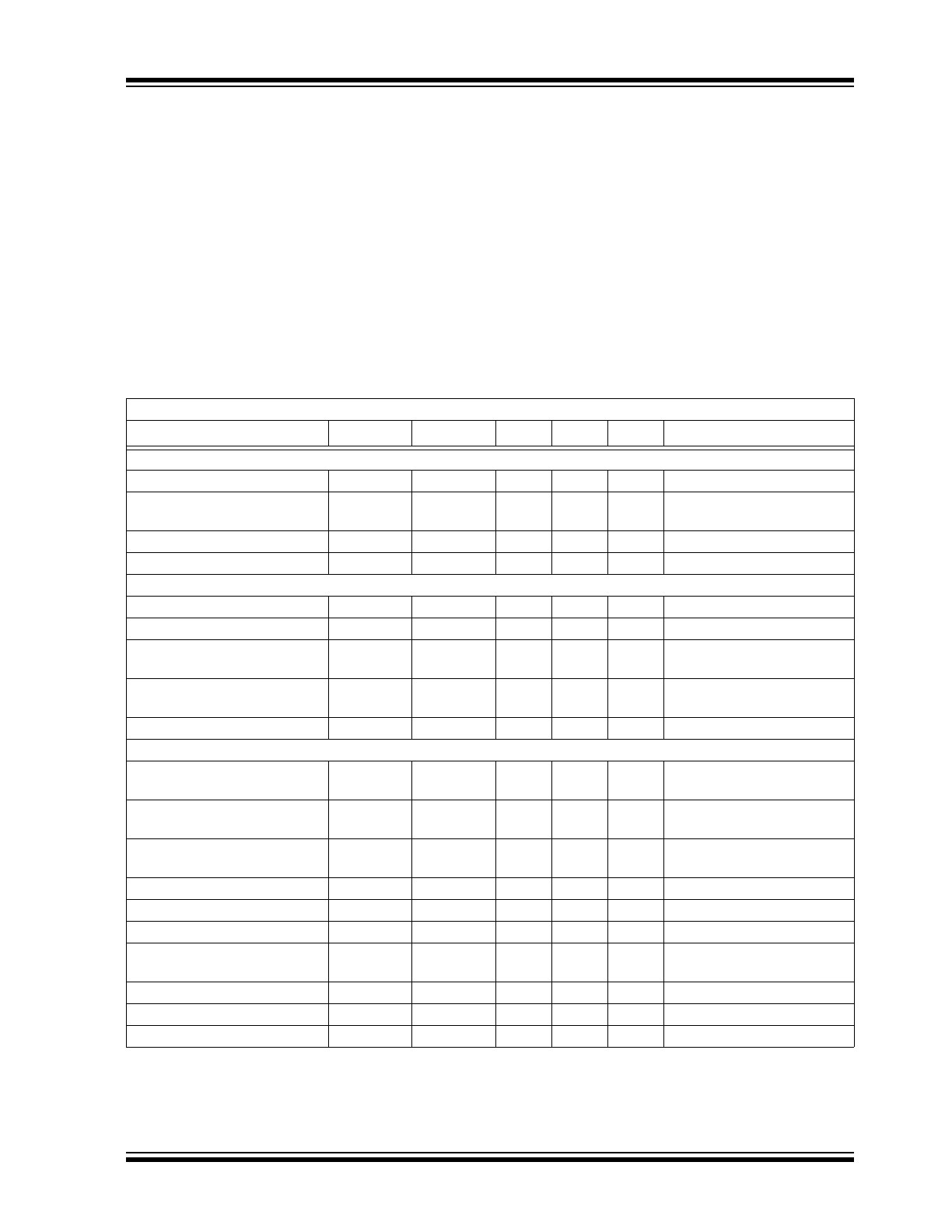
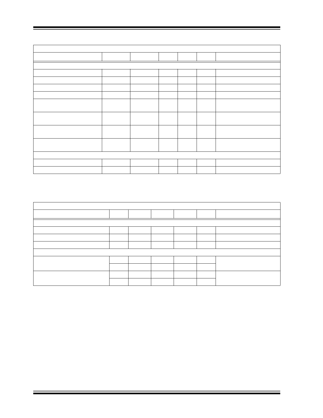
DC CHARACTERISTICS
Electrical Specifications: Unless otherwise noted, V
CC
= 5.0V, T
J
= -40°C to +125°C
Parameters
Sym.
Min.
Typ.
Max.
Units
Conditions
V
CC
Supply Requirements
V
CC
Operating Range
V
CC
4.5
5.0
5.5
V
Bias Supply Voltage
I
VCC
—
45
—
µA
PWM
HI
and PWM
LO
pin
floating
UVLO (Rising V
CC
)
V
UVLO
—
3.50
4.00
V
UVLO Hysteresis
V
HYS
—
500
—
mV
PWM Input Requirements
PWM Input Current
I
PWM
—
7.0
10
µA
V
PWM
= 3.0V
PWM Input Current
I
PWM
—
1.0
—
nA
V
PWM
= 0V
PWM
LO
and PWM
HI
Rising
Threshold
PWM
HI_TH
1.40
1.60
1.80
V
V
CC
= 5.0V
PWM
LO
and PWM
HI
Falling
Threshold
PWM
LO_TH
1.10
1.20
1.30
V
V
CC
= 5.0V
PWM Input Hysteresis
PWM
HYS
—
400
—
mV
V
CC
= 5.0V
Output Requirements
High Output Voltage (HIGHDR
and LOWDR)
V
OH
V
CC
- 0.025
—
—
V
V
CC
= 5.0V
Low Output Voltage (HIGHDR
and LOWDR)
V
OL
—
—
0.025
V
V
CC
= 5.0V
High Drive Source Resistance
R
HI_SRC
—
1.0
2.5
500 mA source current,
Note 1
High Drive Sink Resistance
R
HI_SINK
—
1.0
2.5
500 mA sink current,
Note 1
High Drive Source Current
I
HI_SRC
—
2.0
—
A
Note 1
High Drive Sink Current
I
HI_SINK
—
2.0
—
A
Note 1
Low Drive Source Resistance
R
LO_SRC
—
1.0
2.5
500 mA source current,
Note 1
Low Drive Sink Resistance
R
LO_SINK
—
0.5
1.0
500 mA sink current,
Note 1
Low Drive Source Current
I
LO_SRC
—
2.0
—
A
Note 1
Low Drive Sink Current
I
LO_SINK
—
3.5
—
A
Note 1
Note 1:
Parameter ensured by characterization, not production tested.
2:
See
Figure 4-1
and
Figure 4-2
for parameter definition.
MCP14700
DS22201B-page 6
2009-2013 Microchip Technology Inc.
Switching Times
HIGHDR Rise Time
t
RH
—
10
—
ns
C
L
= 3.3 nF,
Note 1
,
Note 2
LOWDR Rise Time
t
RL
—
10
—
ns
C
L
= 3.3 nF,
Note 1
,
Note 2
HIGHDR Fall Time
t
FH
—
10
—
ns
C
L
= 3.3 nF,
Note 1
,
Note 2
LOWDR Fall Time
t
FL
—
6.0
—
ns
C
L
= 3.3 nF,
Note 1
,
Note 2
HIGHDR Turn-off Propagation
Delay
t
PDLH
20
27
36
ns
No Load,
Note 1
,
Note 2
LOWDR Turn-off Propagation
Delay
t
PDLL
10
17
25
ns
No Load,
Note 1
,
Note 2
HIGHDR Turn-on Propagation
Delay
t
PDHH
20
27
36
ns
No Load,
Note 1
,
Note 2
LOWDR Turn-on Propagation
Delay
t
PDHL
10
17
25
ns
No Load,
Note 1
,
Note 2
Protection Requirements
Thermal Shutdown
T
SHDN
—
147
—
°C
Note 1
Thermal Shutdown Hysteresis
T
SHDN_HYS
—
20
—
°C
Note 1
DC CHARACTERISTICS (CONTINUED)
Electrical Specifications: Unless otherwise noted, V
CC
= 5.0V, T
J
= -40°C to +125°C
Parameters
Sym.
Min.
Typ.
Max.
Units
Conditions
Note 1:
Parameter ensured by characterization, not production tested.
2:
See
Figure 4-1
and
Figure 4-2
for parameter definition.
TEMPERATURE CHARACTERISTICS
Unless otherwise noted, all parameters apply with V
CC
= 5.0V
Parameter
Sym.
Min.
Typ.
Max.
Units
Comments
Temperature Ranges
Maximum Junction Temperature
T
J
—
—
+150
°C
Storage Temperature
T
A
-65
—
+150
°C
Specified Temperature Range
T
A
-40
—
+125
°C
Package Thermal Resistances
Thermal Resistance, 8L-3x3 DFN
JA
—
64
—
°C/W
Typical four-layer board with
vias to ground plane
JC
—
12
—
°C/W
Thermal Resistance, 8L-SOIC
JA
—
163
—
°C/W
JC
—
42
—
°C/W
2009-2013 Microchip Technology Inc.
DS22201B-page 7
MCP14700
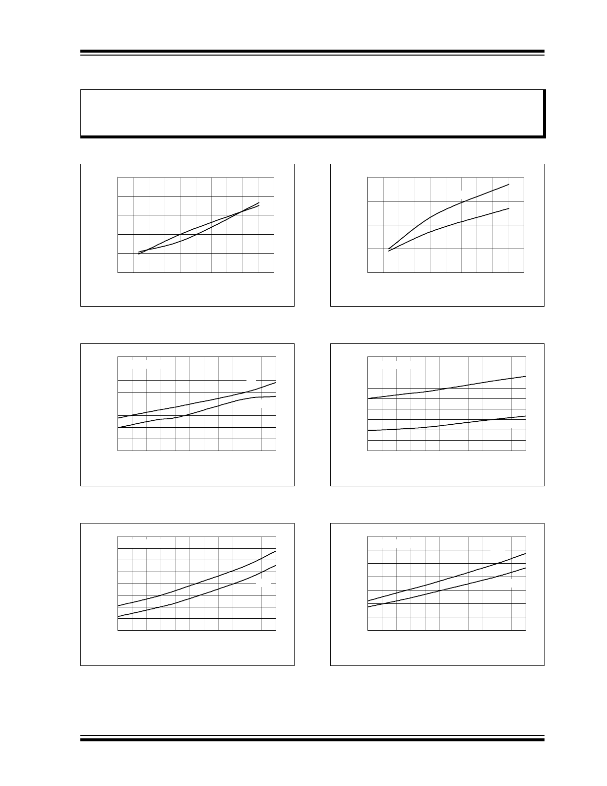
2.0
TYPICAL PERFORMANCE CURVES
Note: Unless otherwise indicated, T
A
= +25°C with V
CC
= 5.0V.
FIGURE 2-1:
Rise Time vs. Capacitive
Load.
FIGURE 2-2:
HIGHDR Rise and Fall Time
vs. Temperature.
FIGURE 2-3:
HIGHDR Propagation Delay
vs. Temperature.
FIGURE 2-4:
Fall Time vs. Capacitive
Load.
FIGURE 2-5:
LOWDR Rise and Fall Time
vs. Temperature.
FIGURE 2-6:
LOWDR Propagation Delay
vs. Temperature.
Note:
The graphs and tables provided following this note are a statistical summary based on a limited number of
samples and are provided for informational purposes only. The performance characteristics listed herein
are not tested or guaranteed. In some graphs or tables, the data presented may be outside the specified
operating range (e.g., outside specified power supply range) and therefore outside the warranted range.
0
5
10
15
20
25
0
1500
3000
4500
6000
7500
Capacitive Load (pF)
R
ise
T
im
e
(n
s)
t
RL
t
RH
6
7
8
9
10
11
12
13
14
-40 -25 -10 5
20 35 50 65 80 95 110 125
Temperature (
o
C)
Ti
m
e
(
n
s)
t
RH
t
FH
C
LOAD
= 3,300 pF
20
22
24
26
28
30
32
34
36
-40 -25 -10 5
20 35 50 65 80 95 110 125
Temperature (
o
C)
P
rop
a
g
at
io
n D
el
ay
(
n
s)
t
PDLH
t
PDHH
C
LOAD
= 3,300 pF
0
2
4
6
8
10
12
14
16
0
1500
3000
4500
6000
7500
Capacitive Load (pF)
F
all
T
im
e
(n
s)
t
FL
t
FH
5
6
7
8
9
10
11
12
13
14
-40 -25 -10 5
20 35 50 65 80 95 110 125
Temperature (
o
C)
Ti
m
e
(
n
s)
t
RL
t
FL
C
LOAD
= 3,300 pF
10
12
14
16
18
20
22
24
-40 -25 -10 5
20 35 50 65 80 95 110 125
Temperature (
o
C)
P
rop
a
g
at
io
n D
el
ay
(
n
s)
t
PDHL
t
PDLL
C
LOAD
= 3,300 pF
MCP14700
DS22201B-page 8
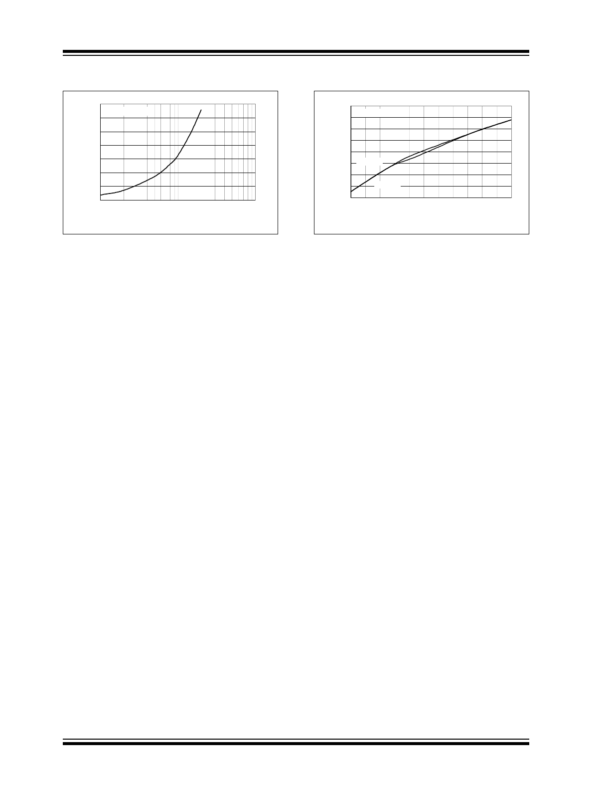
2009-2013 Microchip Technology Inc.
Note: Unless otherwise indicated, T
A
= +25°C with V
CC
= 5.0V.
FIGURE 2-7:
Supply Current vs.
Frequency.
FIGURE 2-8:
Supply Current vs.
Temperature.
0
10
20
30
40
50
60
70
100
1000
10000
Frequency (kHz)
S
u
p
p
ly C
u
rr
en
t
(m
A
)
C
LOAD
= 3,300 pF
40
41
42
43
44
45
46
47
48
-40 -25 -10
5
20 35 50 65 80 95 110 125
Temperature (°C)
Su
p
p
ly
C
u
rr
e
n
t
(µ
A
)
PWM = 1
PWM = 0
C
LOAD
= 3,300 pF
2009-2013 Microchip Technology Inc.
DS22201B-page 9
MCP14700
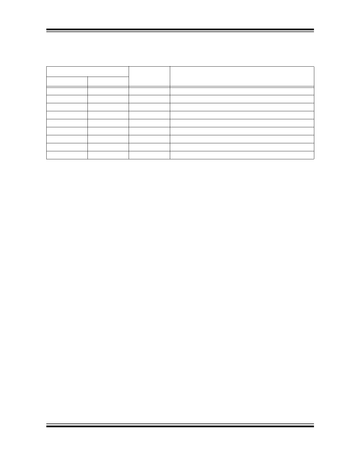
3.0
PIN DESCRIPTIONS
The descriptions of the pins are listed in
Table 3-1
.
3.1
Switch Node (PHASE)
The PHASE pin provides a return path for the high-side
gate driver. The source of the high-side and the drain of
the low-side power MOSFETs are connected to this
pin.
3.2
High-Side PWM Control Input
Signal (PWM
HI
)
The PWM input signal to control the high-side power
MOSFET is applied to the PWM
HI
pin. A logic high on
the PWM
HI
pin causes the HIGHDR pin to also
transition high.
3.3
Low-Side PWM Control Input
Signal (PWM
LO
)
The PWM input signal to control the low-side power
MOSFET is applied to the PWM
LO
pin. A logic high on
the PWM
LO
pin causes the LOWDR pin to also
transition high.
3.4
Ground (GND)
The GND pin provides ground for the MCP14700
circuitry. It should have a low-impedance connection to
the bias supply source return. High peak currents will
flow out the GND pin when the low-side power
MOSFET is being turned off.
3.5
Low-side Gate Drive (LOWDR)
The LOWDR pin provides the gate drive signal to
control the low-side power MOSFET. The gate of the
low-side power MOSFET is connected to this pin.
3.6
Supply Input Voltage (V
CC
)
The V
CC
pin provides bias to the MCP14700 device. A
bypass capacitor is to be placed between this pin and
the GND pin. This capacitor should be placed as close
to the MCP14700 as possible.
3.7
Floating Bootstrap Supply (BOOT)
The BOOT pin is the floating bootstrap supply pin for
the high-side gate drive. A capacitor is connected
between this pin and the PHASE pin to provide the
necessary charge to turn on the high-side power
MOSFET.
3.8
High-Side Gate Drive (HIGHDR)
The HIGHDR pin provides the gate drive signal to
control the high-side power MOSFET. The gate of the
high-side power MOSFET is connected to this pin.
3.9
Exposed Metal Pad (EP)
The exposed metal pad of the DFN package is not
internally connected to any potential. Therefore, this
pad can be connected to a ground plane or other
copper plane on a printed circuit board to aid in heat
removal from the package.
TABLE 3-1:
PIN FUNCTION TABLE
MCP14700
Symbol
Description
3x3 DFN
SOIC
1
1
PHASE
Switch Node
2
2
PWM
HI
High-Side PWM Control Input Signal
3
3
PWM
LO
Low-Side PWM Control Input Signal
4
4
GND
Ground
5
5
LOWDR
Low-side Gate Drive
6
6
V
CC
Supply Input Voltage
7
7
BOOT
Floating Bootstrap Supply
8
8
HIGHDR
High-Side Gate Drive
9
—
EP
Exposed Metal Pad

MCP14700
DS22201B-page 10
2009-2013 Microchip Technology Inc.
NOTES: