

2006-2016 Microchip Technology Inc.
DS20002019C-page 1
MCP1406/07
Features
• High Peak Output Current: 6.0A (typical)
• Low Shoot-Through/Cross-Conduction Current in
Output Stage
• Wide Input Supply Voltage Operating Range:
- 4.5V to 18V
• High Capacitive Load Drive Capability:
- 2500 pF in 20 ns
- 6800 pF in 40 ns
• Short Delay Times: 40 ns (typical)
• Matched Rise/Fall Times
• Low Supply Current:
- With Logic ‘1’ Input – 130 µA (typical)
- With Logic ‘0’ Input – 35 µA (typical)
• Latch-Up Protected: Will Withstand 1.5A Reverse
Current
• Logic Input Will Withstand Negative Swing up to 5V
• Pin compatible with the TC4420/TC4429 devices
• Space-saving 8-Pin SOIC, PDIP and
8-Pin 6 x 5 mm DFN Packages
Applications
• Switch Mode Power Supplies
• Pulse Transformer Drive
• Line Drivers
• Motor and Solenoid Drive
General Description
The MCP1406/07 devices are a family of
buffers/MOSFET drivers that feature a single-output
with 6A peak drive current capability, low shoot-through
current, matched rise/fall times and propagation delay
times. These devices are pin-compatible and are
improved versions of the TC4420/TC4429 MOSFET
drivers.
The MCP1406/07 MOSFET drivers can easily charge
and discharge 2500 pF gate capacitance in under
20 ns, provide low enough impedances (in both the ON
and OFF states) to ensure that intended state of the
MOSFETs will not be affected, even by large transients.
The input to the MCP1406/07 may be driven directly
from either TTL or CMOS (3V to 18V).
These devices are highly latch-up resistant under any
conditions that fall within their power and voltage
ratings. They are not subject to damage when up to 5V
of noise spiking (of either polarity) occurs on the ground
pin. All terminals are fully protected against
electrostatic discharge (ESD), up to 2.0 kV (HBM) and
400V (MM).
The MCP1406/07 single-output 6A MOSFET driver
family is offered in both surface-mount and
pin-through-hole packages with a -40°C to +125°C
temperature rating, making it useful in any wide
temperature range application.
6A High-Speed Power MOSFET Drivers
MCP1406/07
DS20002019C-page 2
2006-2016 Microchip Technology Inc.
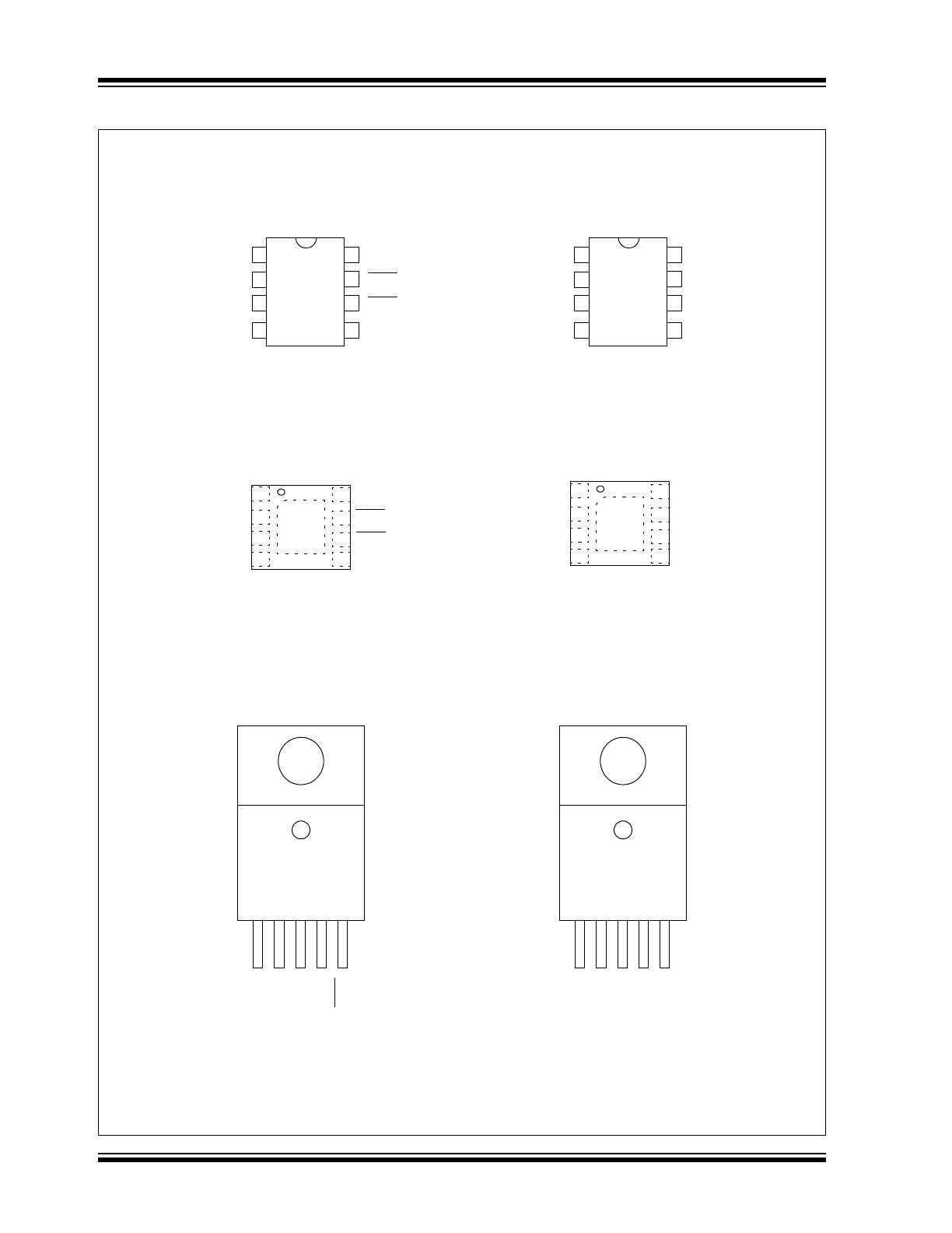
Package Types
1
2
3
4
5
6
7
8
V
DD
V
DD
OUT
OUT
GND
GND
INPUT
NC
8-Pin PDIP/SOIC
MCP1407
MCP1406
V
DD
OUT
OUT
GND
V
DD
GND
INPUT
NC
5-Pin TO-220
MCP1407
MCP1406
V
DD
OUT
OUT
GND
Tab is common to V
DD
Note 1: Duplicate pins must both be connected for proper operation.
2: Exposed pad of the DFN package is electrically isolated; see
Table 3-1
.
1
2
3
4
5
6
7
8
V
DD
GND
INPUT
NC
V
DD
GND
INPUT
OUT
GND
1 2 3 4 5
MCP1406
V
DD
GND
INPUT
OUT
GND
1 2 3 4 5
MCP1407
1
2
3
4
8
7
6
5
EP
9
V
DD
GND
INPUT
NC
V
DD
OUT
OUT
GND
1
2
3
4
8
7
6
5
EP
9
8-Pin 6x5 DFN-S
(
2
)
2006-2016 Microchip Technology Inc.
DS20002019C-page 3
MCP1406/07
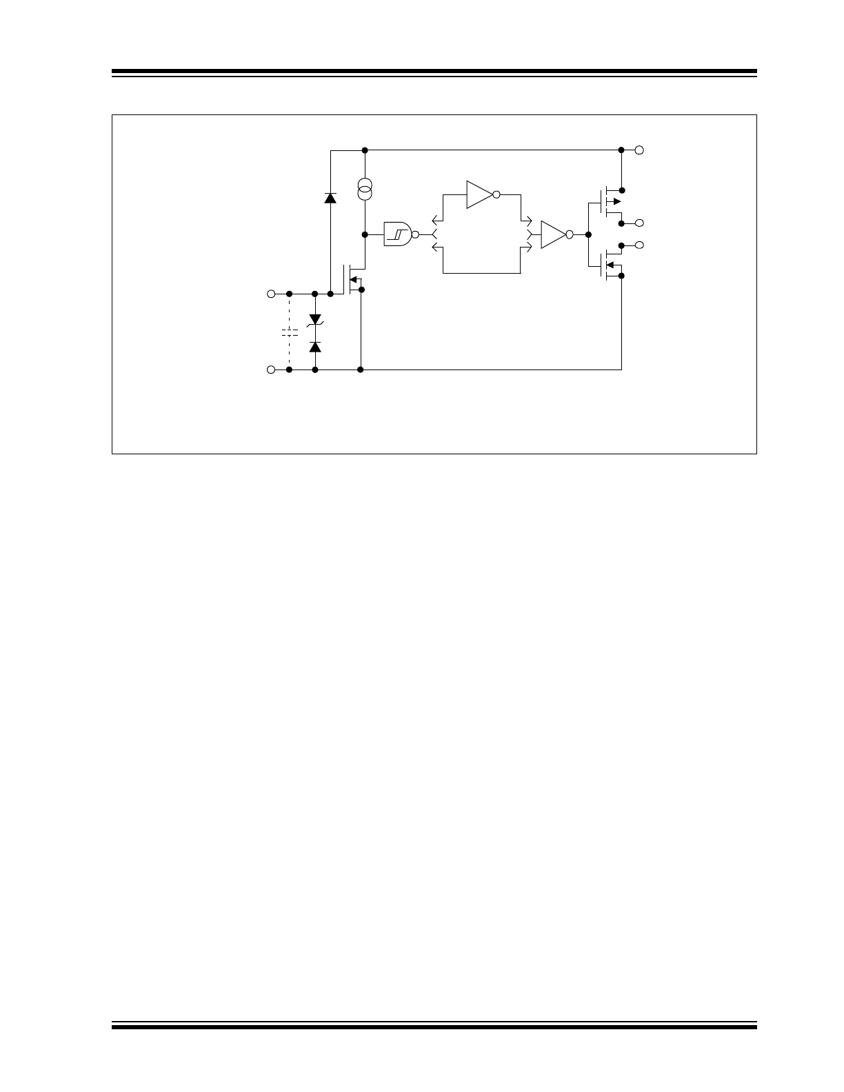
Functional Block Diagram
(1)
Effective
Input C = 25 pF
MCP1406 Inverting
MCP1407 Non-Inverting
Input
GND
V
DD
300 mV
4.7V
Inverting
Non-Inverting
Note 1: Unused inputs should be grounded.
130 µA
Output
Output
MCP1406/07
DS20002019C-page 4
2006-2016 Microchip Technology Inc.
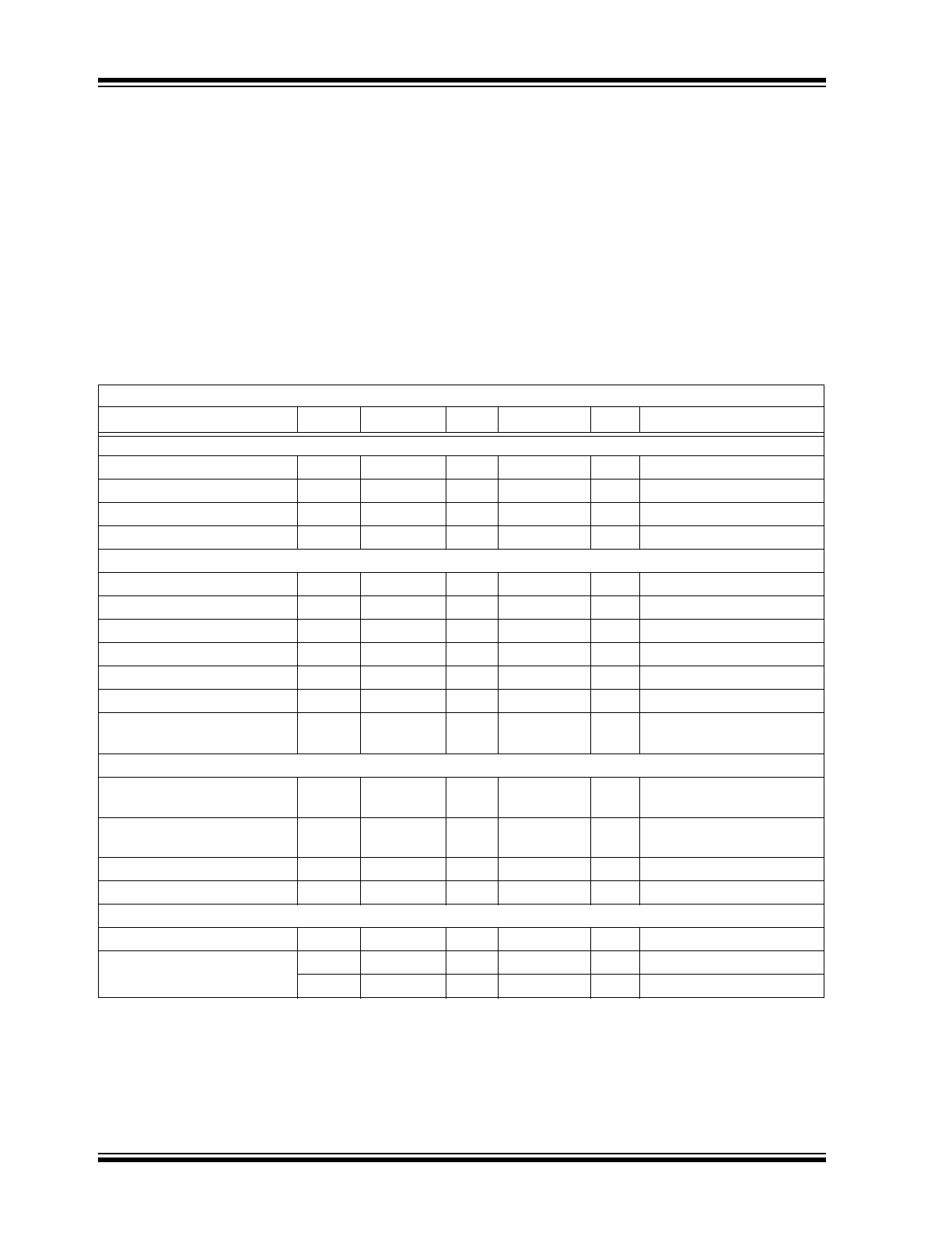
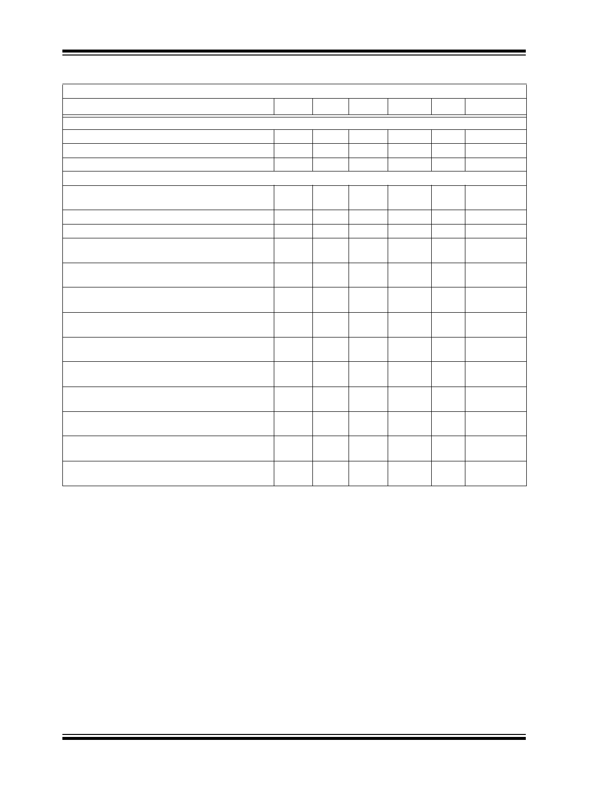
1.0
ELECTRICAL
CHARACTERISTICS
Absolute Maximum Ratings †
Supply Voltage ................................................................+20V
Input Voltage ..................................(V
DD
+0.3V) to (GND -5V)
Input Current (V
IN
> V
DD
) ..............................................50 mA
Package Power Dissipation (TA <= +70°C)
DFN-S .......................................................................2.5W
PDIP..........................................................................1.2W
SOIC .......................................................................0.83W
TO-220 ......................................................................3.9W
ESD Protection on all Pins ................2 kV (HBM), 400V (MM)
† Notice: Stresses above those listed under “Maximum
Ratings” may cause permanent damage to the device.
This is a stress rating only and functional operation of
the device at those or any other conditions above those
indicated in the operational sections of this
specification is not intended. Exposure to maximum
rating conditions for extended periods may affect
device reliability.
DC CHARACTERISTICS
Electrical Specifications: Unless otherwise indicated, T
A
= +25°C, with 4.5V
V
DD
18V.
Parameters
Sym.
Min.
Typ.
Max.
Units
Conditions
Input
Logic ‘1’, High Input Voltage
V
IH
2.4
1.8
—
V
Logic ‘0’, Low Input Voltage
V
IL
—
1.3
0.8
V
Input Current
I
IN
–10
—
10
µA
0V
V
IN
V
DD
Input Voltage
V
IN
-5
—
V
DD
+ 0.3
V
Output
High Output Voltage
V
OH
V
DD
– 0.025
—
—
V
DC Test
Low Output Voltage
V
OL
—
—
0.025
V
DC Test
Output Resistance, High
R
OH
—
2.1
2.8
I
OUT
= 10 mA, V
DD
= 18V
Output Resistance, Low
R
OL
—
1.5
2.5
I
OUT
= 10 mA, V
DD
= 18V
Peak Output Current
I
PK
—
6
—
A
V
DD
18V (
Note 1
)
Continuous Output Current
I
DC
1.3
A
Note 1
,
Note 2
Latch-Up Protection Withstand
Reverse Current
I
REV
—
1.5
—
A
Duty cycle
2%, t 300 µs
Switching Time (
Note 3
)
Rise Time
t
R
—
20
30
ns
Figure 4-1
,
Figure 4-2
C
L
= 2500 pF
Fall Time
t
F
—
20
30
ns
Figure 4-1
,
Figure 4-2
C
L
= 2500 pF
Delay Time
t
D1
—
40
55
ns
Figure 4-1
,
Figure 4-2
Delay Time
t
D2
—
40
55
ns
Figure 4-1
,
Figure 4-2
Power Supply
Supply Voltage
V
DD
4.5
—
18.0
V
Power Supply Current
I
S
—
130
250
µA
V
IN
= 3V
I
S
—
35
100
µA
V
IN
= 0V
Note 1: Tested during characterization, not production tested.
2: Valid for AT (TO-220) and MF (DFN-S) packages only. T
A
= +25°C
3: Switching times ensured by design.
2006-2016 Microchip Technology Inc.
DS20002019C-page 5
MCP1406/07
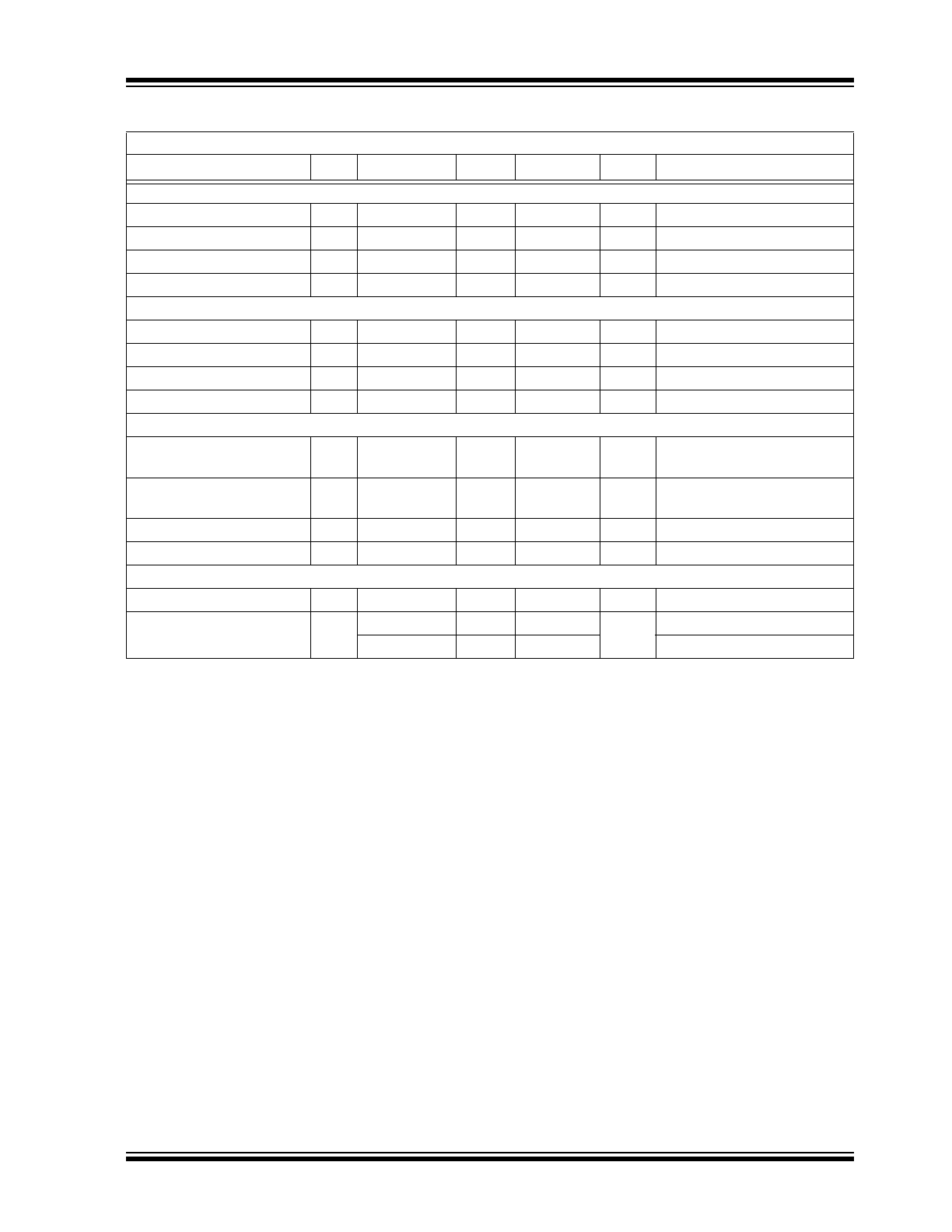
DC CHARACTERISTICS (OVER OPERATING TEMPERATURE RANGE)
Electrical Specifications: Unless otherwise indicated, operating temperature range with 4.5V
V
DD
18V.
Parameters
Sym.
Min.
Typ.
Max.
Units
Conditions
Input
Logic ‘1’, High Input Voltage
V
IH
2.4
—
—
V
Logic ‘0’, Low Input Voltage
V
IL
—
—
0.8
V
Input Current
I
IN
-10
—
+10
µA
0V
V
IN
V
DD
Input Voltage
V
IN
-5
—
V
DD
+0.3
V
Output
High Output Voltage
V
OH
V
DD
– 0.025
—
—
V
DC TEST
Low Output Voltage
V
OL
—
—
0.025
V
DC TEST
Output Resistance, High
R
OH
—
3.0
5.0
I
OUT
= 10 mA, V
DD
= 18V
Output Resistance, Low
R
OL
—
2.3
5.0
I
OUT
= 10 mA, V
DD
= 18V
Switching Time (
Note 1
)
Rise Time
t
R
—
25
40
ns
Figure 4-1
,
Figure 4-2
C
L
= 2500 pF
Fall Time
t
F
—
25
40
ns
Figure 4-1
,
Figure 4-2
C
L
= 2500 pF
Delay Time
t
D1
—
50
65
ns
Figure 4-1
,
Figure 4-2
Delay Time
t
D2
—
50
65
ns
Figure 4-1
,
Figure 4-2
Power Supply
Supply Voltage
V
DD
4.5
—
18.0
V
Power Supply Current
I
S
—
200
500
µA
V
IN
= 3V
—
50
150
V
IN
= 0V
Note 1: Switching times ensured by design.
MCP1406/07
DS20002019C-page 6
2006-2016 Microchip Technology Inc.
TEMPERATURE CHARACTERISTICS
Electrical Specifications: Unless otherwise noted, all parameters apply with 4.5V
V
DD
18V.
Parameters
Sym.
Min.
Typ.
Max.
Units
Conditions
Temperature Ranges
Specified Temperature Range
T
A
-40
—
+125
°C
Maximum Junction Temperature
T
J
—
—
+150
°C
Storage Temperature Range
T
A
-65
—
+150
°C
Package Thermal Resistances
Junction-to-Ambient Thermal Resistance,
8-L 6x5 DFN
JA
—
31.8
—
°C/W
Note 1
Junction-to-Ambient Thermal Resistance, 8-L PDIP
JA
—
65.2
—
°C/W
Note 1
Junction-to-Ambient Thermal Resistance, 8-L SOIC
JA
—
96.3
—
°C/W
Note 1
Junction-to-Ambient Thermal Resistance,
5-L TO-220
JA
—
20.1
—
°C/W
Note 1
Junction-to-Case (Bottom) Thermal Resistance,
5-L TO-220
JC(BOT)
3.2
—
°C/W
Note 2
Junction-to-Top Characterization Parameter,
8-L 6x5 DFN
JT
0.2
—
°C/W
Note 1
Junction-to-Top Characterization Parameter,
8-L PDIP
JT
8.8
—
°C/W
Note 1
Junction-to-Top Characterization Parameter,
8-L SOIC
JT
3.2
—
°C/W
Note 1
Junction-to-Top Characterization Parameter,
5-L TO-220
JT
3.6
—
°C/W
Note 1
Junction-to-Board Characterization Parameter,
8-L 6x5 DFN
JB
15.5
—
°C/W
Note 1
Junction-to-Board Characterization Parameter,
8-L PDIP
JB
36.1
—
°C/W
Note 1
Junction-to-Board Characterization Parameter,
8-L SOIC
JB
60.7
—
°C/W
Note 1
Junction-to-Board Characterization Parameter,
5-L TO-220
JB
4.0
—
°C/W
Note 1
Note 1: Parameter is determined using a High 2S2P 4-layer board, as described in JESD 51-7, as well as in JESD
51-5, for packages with exposed pads.
2: Parameter is determined using a 1S0P 2-layer board with a cold plate attached to indicated location.
2006-2016 Microchip Technology Inc.
DS20002019C-page 7
MCP1406/07
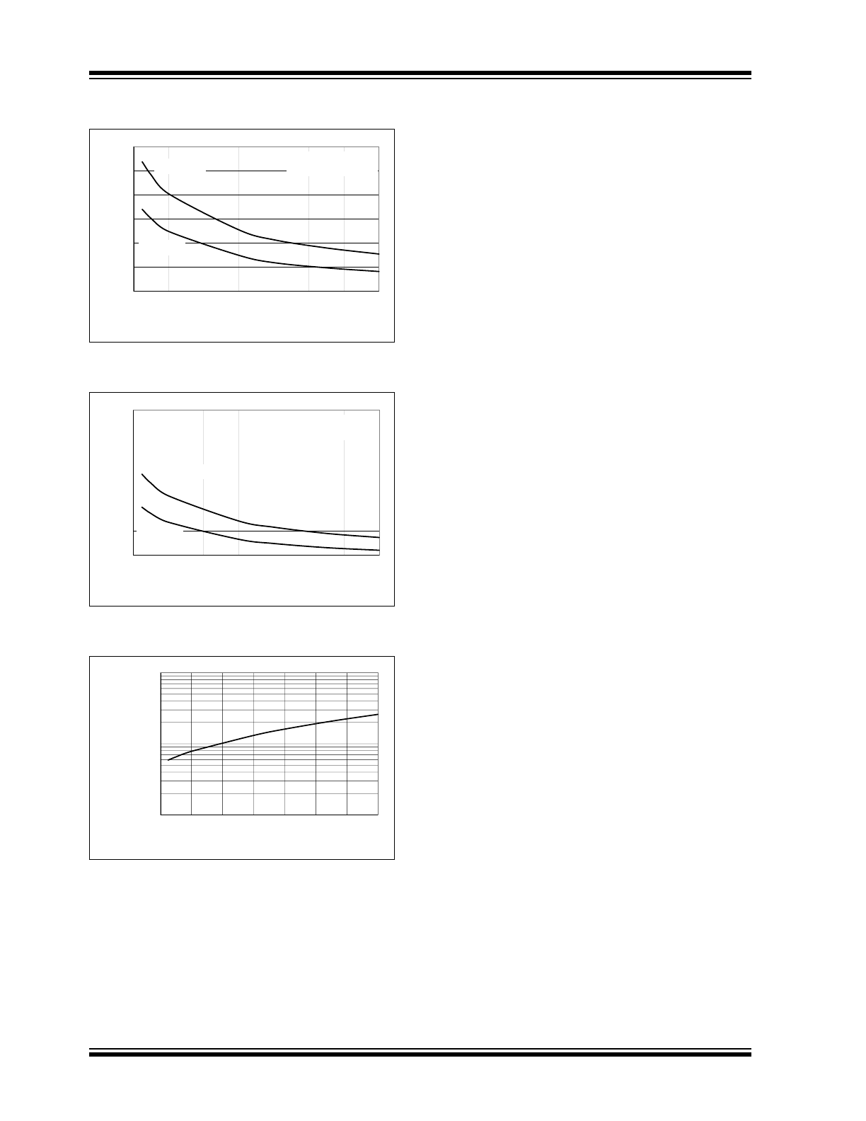
2.0
TYPICAL PERFORMANCE CURVES
Note: Unless otherwise indicated, T
A
= +25°C with 4.5V
V
DD
18V.
FIGURE 2-1:
Rise Time vs. Supply
Voltage.
FIGURE 2-2:
Rise Time vs. Capacitive
Load.
FIGURE 2-3:
Rise and Fall Times vs.
Temperature.
FIGURE 2-4:
Fall Time vs. Supply
Voltage.
FIGURE 2-5:
Fall Time vs. Capacitive
Load.
FIGURE 2-6:
Propagation Delay vs.
Supply Voltage.
Note:
The graphs and tables provided following this note are a statistical summary based on a limited number of
samples and are provided for informational purposes only. The performance characteristics listed herein
are not tested or guaranteed. In some graphs or tables, the data presented may be outside the specified
operating range (e.g., outside specified power supply range) and therefore outside the warranted range.
0
20
40
60
80
100
120
4
6
8
10
12
14
16
18
Supply Voltage (V)
R
ise
T
ime
(n
s)
100 pF
4,700 pF
1,000 pF
6,800 pF
2,500 pF
10,000 pF
8,200 pF
0
10
20
30
40
50
60
70
80
100
1000
10000
Capacitive Load (pF)
Ri
se Ti
me (n
s)
5V
15V
10V
0
5
10
15
20
25
30
-40 -25 -10 5
20 35 50 65 80 95 110 125
Temperature (
o
C)
R
is
e an
d F
all
Ti
me
(n
s)
V
DD
= 18V
t
RISE
t
FALL
0
10
20
30
40
50
60
70
80
4
6
8
10
12
14
16
18
Supply Voltage (V)
F
all
Ti
me
(n
s)
100 pF
4,700 pF
1,000 pF
6,800 pF
2,500 pF
10,000 pF
8,200 pF
0
10
20
30
40
50
60
70
100
1000
10000
Capacitive Load (pF)
F
all Tim
e (n
s)
5V
15V
10V
35
45
55
65
75
85
4
6
8
10
12
14
16
18
Supply Voltage (V)
Pr
op
ag
at
io
n
De
la
y
(n
s)
V
IN
= 5V
t
D1
t
D2
MCP1406/07
DS20002019C-page 8
2006-2016 Microchip Technology Inc.
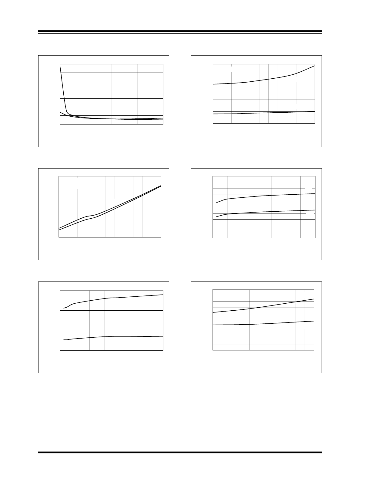
Note: Unless otherwise indicated, T
A
= +25°C with 4.5V
V
DD
18V.
FIGURE 2-7:
Propagation Delay Time vs.
Input Amplitude.
FIGURE 2-8:
Propagation Delay Time vs.
Temperature.
FIGURE 2-9:
Quiescent Current vs.
Supply Voltage.
FIGURE 2-10:
Quiescent Current vs.
Temperature.
FIGURE 2-11:
Input Threshold vs. Supply
Voltage.
FIGURE 2-12:
Input Threshold vs.
Temperature.
25
50
75
100
125
150
175
200
2
3
4
5
6
7
8
9
10
Input Amplitude (V)
Prop
ag
ati
o
n
D
e
la
y
(ns
)
V
DD
= 12V
t
D1
t
D2
30
35
40
45
50
55
-40 -25 -10 5
20 35 50 65 80 95 110 125
Temperature (
o
C)
Prop
aga
tio
n Delay
(n
s)
V
DD
= 18V
V
IN
= 5V
t
D1
t
D2
0
20
40
60
80
100
120
140
160
180
4
6
8
10
12
14
16
18
Supply Voltage (V)
Qu
ie
sc
e
n
t C
u
rre
nt
(µA
)
INPUT = 1
INPUT = 0
0
50
100
150
200
250
-40 -25 -10 5
20 35 50 65 80 95 110 125
Temperature (
o
C)
Q
u
ie
sc
en
t Cu
rr
en
t (µA)
Input = Low
V
DD
= 18V
Input = High
1
1.1
1.2
1.3
1.4
1.5
1.6
1.7
1.8
1.9
2
4
6
8
10
12
14
16
18
Supply Voltage (V)
Inpu
t Thres
hol
d
(V)
V
HI
V
LO
1
1.1
1.2
1.3
1.4
1.5
1.6
1.7
1.8
1.9
2
-40 -25 -10 5
20 35 50 65 80 95 110 125
Temperature (
o
C)
Inp
u
t Th
re
shol
d (V)
V
DD
= 12V
V
HI
V
LO
2006-2016 Microchip Technology Inc.
DS20002019C-page 9
MCP1406/07
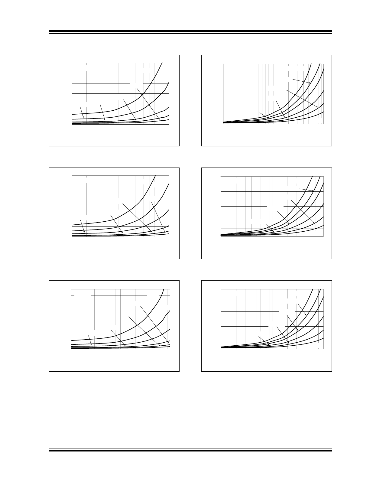
Note: Unless otherwise indicated, T
A
= +25°C with 4.5V
V
DD
18V.
FIGURE 2-13:
Supply Current vs.
Capacitive Load.
FIGURE 2-14:
Supply Current vs.
Capacitive Load.
FIGURE 2-15:
Supply Current vs.
Capacitive Load.
FIGURE 2-16:
Supply Current vs.
Frequency.
FIGURE 2-17:
Supply Current vs.
Frequency.
FIGURE 2-18:
Supply Current vs.
Frequency.
0
25
50
75
100
125
150
100
1000
10000
Capacitive Load (pF)
S
u
p
p
ly
C
u
rr
en
t
(m
A
)
500 kHz
1 MHz
200 kHz
100 kHz
V
DD
= 18V
50 kHz
0
25
50
75
100
125
150
100
1000
10000
Capacitive Load (pF)
Su
pp
ly Cu
rren
t (m
A)
500 kHz
1 MHz
200 kHz
100 kHz
V
DD
= 12V
50 kHz
2 MHz
0
10
20
30
40
50
60
70
80
90
100
100
1000
10000
Capacitive Load (pF)
S
uppl
y
Curre
nt
(
m
A)
500 kHz
1 MHz
200 kHz
100 kHz
V
DD
= 6V
50 kHz
2 MHz
0
20
40
60
80
100
120
10
100
1000
Frequency (kHz)
S
uppl
y C
u
rrent (mA)
100 pF
4,700 pF
1,000 pF
6,800 pF
V
DD
= 18V
2,500 pF
10,000 pF
0
10
20
30
40
50
60
70
80
10
100
1000
Frequency (kHz)
S
upp
ly
Cu
rre
nt
(mA)
100 pF
4,700 pF
1,000 pF
6,800 pF
V
DD
= 12V
2,500 pF
10,000 pF
0
5
10
15
20
25
30
35
40
10
100
1000
Frequency (kHz)
S
uppl
y
Curre
nt
(
m
A)
100 pF
4,700 pF
1,000 pF
6,800 pF
V
DD
= 6V
2,500 pF
10,000 pF
MCP1406/07
DS20002019C-page 10
2006-2016 Microchip Technology Inc.
Note: Unless otherwise indicated, T
A
= +25°C with 4.5V
V
DD
18V.
FIGURE 2-19:
Output Resistance
(Output High) vs. Supply Voltage.
FIGURE 2-20:
Output Resistance
(Output Low) vs. Supply Voltage.
FIGURE 2-21:
Crossover Energy vs.
Supply Voltage.
1
2
3
4
5
6
7
4
6
8
10
12
14
16
18
Supply Voltage (V)
R
OUT-HI
(
:
)
V
IN
= 2.5V (MCP1407)
V
IN
= 0V (MCP1406)
T
J
= +125
o
C
T
J
= +25
o
C
1
2
3
4
5
6
7
4
6
8
10
12
14
16
18
Supply Voltage (V)
R
OUT-LO
(
:
)
V
IN
= 0V (MCP1407)
V
IN
= 2.5V (MCP1406)
T
J
= +125
o
C
T
J
= +25
o
C
1.00
10.00
100.00
4
6
8
10
12
14
16
18
Crossover Energy
(nA
∗
sec)
Supply Voltage (V)