
2005-2012 Microchip Technology Inc.
DS21985D-page 1
MCP131X/2X
Features:
• Low Supply Current: 1 µA (Typical),10 µA (Max.)
• Precision Monitoring Trip Point Options:
- 2.9V and 4.6V (Standard Offerings)
- 2.0V to 4.7V in 100 mV Increments,
(Contact the local Microchip Sales Office)
• Resets Microcontroller in a Power-loss Event
• Reset Delay Time-Out Option:
- 1.4 ms, 30 ms, 200 ms, or 1.6s (Typical)
• Watchdog Timer Input Time-Out Options:
- 6.3 ms, 102 ms, 1.6s, or 25.6s (Typical)
• Manual Reset (MR) Input (Active-low)
• Single and Complementary Reset Output(s)
• Reset Output Options:
- Push-Pull (Active-high or Active-low)
- Open-Drain (Internal or External Pull-up)
• Temperature Range:
- -40°C to +85°C for Trip Points 2.0 to 2.4V and,
- -40°C to + 125°C for Trip Points > 2.5V
• Voltage Range: 1.0V to 5.5V
• Lead Free Packaging
Description:
The MCP131X/2X are voltage supervisor devices
designed to keep a microcontroller in Reset until the
system voltage has reached and stabilized at the
proper level for reliable system operation. The table
below shows the available features for these devices.
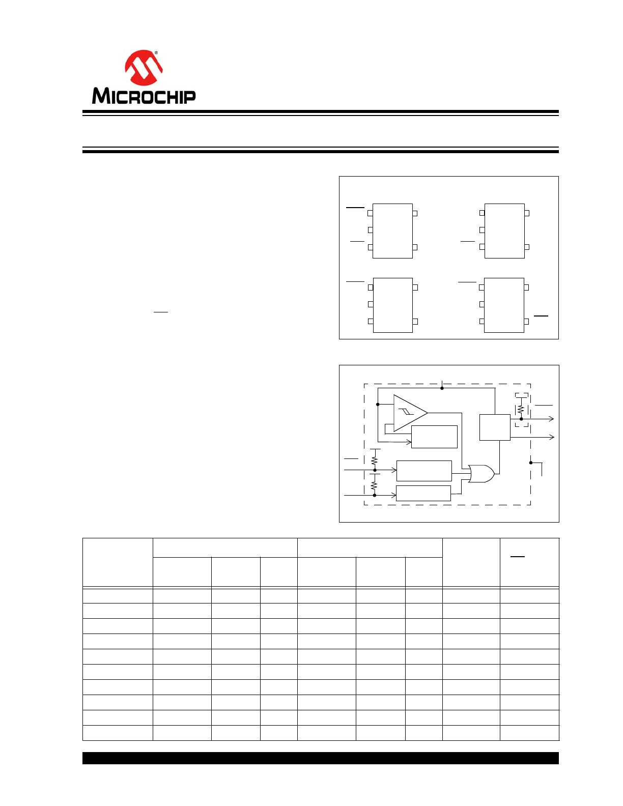
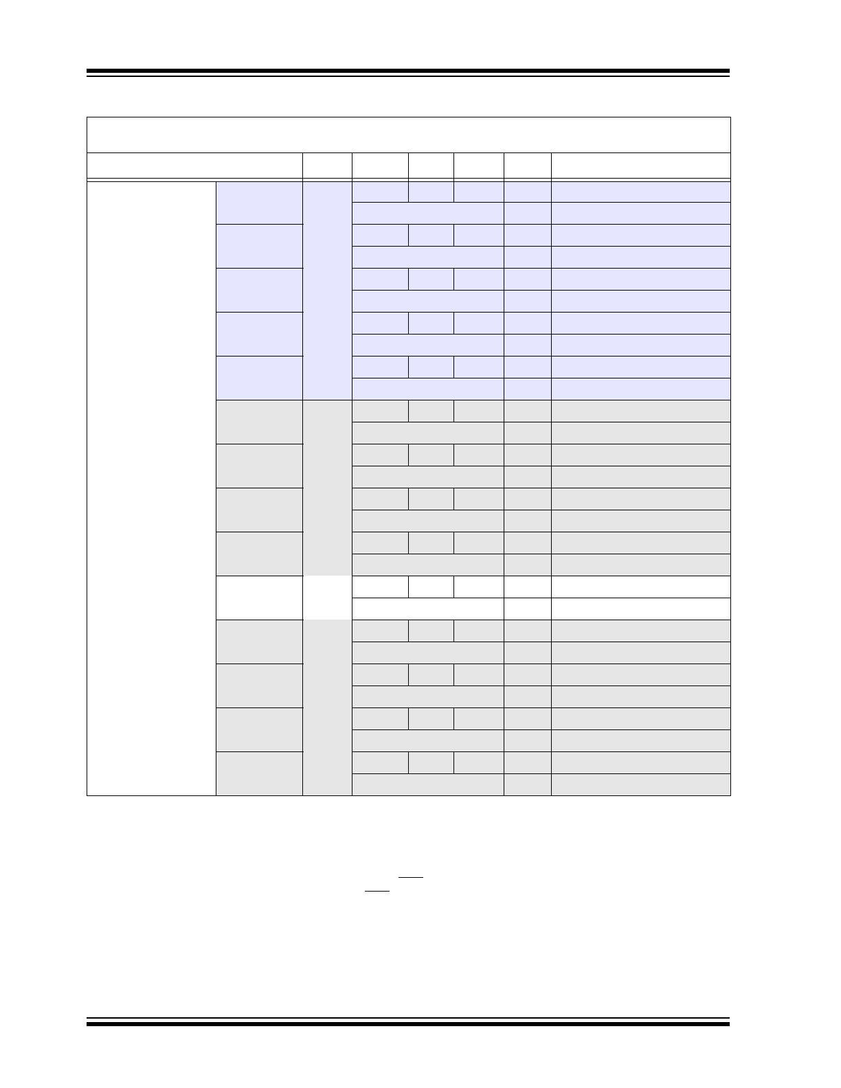
Package Types
Block Diagram
Device Features
1
2
3
5
4
MCP1317
1
2
3
5
4
MCP1318/18M/21
1
2
3
5
4
MCP1319/19M/22
1
2
3
5
4
MCP1316/16M/20
SOT-23-5
RST
RST
V
SS
MR
WDI
V
DD
V
DD
RST
V
SS
MR
WDI
V
SS
RST
WDI
V
DD
RST
V
SS
RST
MR
V
DD
V
DD
Comparator
+
–
Output
Driver
RST
Reference
V
SS
RST
Noise Filter
Watchdog
MR
WDI
Note: Features available depend on the device.
Voltage
Device
Reset Output A
Reset Output B
WDI Input
MR Input
Type
Pull-up
Resistor
Active
Level
Type
Pull-up
Resistor
Active
Level
MCP1316
Push-Pull
—
Low
—
—
—
Yes
Yes
MCP1316M
Open-Drain
Internal
Low
—
—
—
Yes
Yes
MCP1317
Push-Pull
—
High
—
—
—
Yes
Yes
MCP1318
Push-Pull
—
Low
Push-Pull
—
High
Yes
No
MCP1318M
Open-Drain
Internal
Low
Push-Pull
—
High
Yes
No
MCP1319
Push-Pull
—
Low
Push-Pull
—
High
No
Yes
MCP1319M
Open-Drain
Internal
Low
Push-Pull
—
High
No
Yes
MCP1320
Open-Drain
External
Low
—
—
—
Yes
Yes
MCP1321
Open-Drain
External
Low
Push-Pull
—
High
Yes
No
MCP1322
Open-Drain
External
Low
Push-Pull
—
High
No
Yes
Voltage Supervisor

MCP131X/2X
DS21985D-page 2
2005-2012 Microchip Technology Inc.
NOTES:
2005-2012 Microchip Technology Inc.
DS21985D-page 3
MCP131X/2X
1.0
ELECTRICAL
CHARACTERISTICS
Absolute Maximum Ratings†
Supply Voltage (V
DD
to V
SS
) . . . . . . . . . . . . . . . . . . . . . . 7.0V
Input current (V
DD
) . . . . . . . . . . . . . . . . . . . . . . . . . . . .10 mA
Output current (RST) . . . . . . . . . . . . . . . . . . . . . . . . . .10 mA
Voltage on all inputs and outputs, except Open-Drain RST
(with no internal pull-up resistor), w.r.t. V
SS
. .-0.6V to (V
DD
+
1.0V)
Voltage on Open-Drain RST
(with no internal pull-up resistor) w.r.t. V
SS
. . -0.6V to 13.5V
Storage temperature . . . . . . . . . . . . . . . . . . .-65°C to +150°C
Ambient temp. with power applied . . . . . . . .-40°C to +125°C
Maximum Junction temp. with power applied . . . . . . . +150°C
Power Dissipation (T
A
+70°C):
5-Pin SOT-23A .......................................................240 mW
ESD protection on all pins
4 kV
† Notice: Stresses above those listed under “Maximum Rat-
ings” may cause permanent damage to the device. This is a
stress rating only and functional operation of the device at
those or any other conditions above those indicated in the
operational listings of this specification is not implied. Expo-
sure to maximum rating conditions for extended periods may
affect device reliability.
DC CHARACTERISTICS
Electrical Specifications: Unless otherwise indicated, all limits are specified for V
DD
= 1V to 5.5V, R
PU
= 100 k
(only MCP1320, MCP1321 and MCP1322), T
A
= -40°C to +125°C.
Parameters
Sym
Min
Typ
Max
Units
Conditions
Operating Voltage Range
V
DD
1.0
—
5.5
V
Specified V
DD
Value to V
OUT
Low
V
DD
1.0
—
—
V
I
RST
= 10 µA, V
RST
< 0.3V
Operating Current:
I
DD
—
5
10
µA
Watchdog Timer Active
—
1
2
µA
Watchdog Timer Inactive
—
1
2
µA
V
DD
< V
TRIP
—
5
10
µA
Reset Delay Timer Active
Note 1:
Trip point is ±1.5% from typical value.
2:
Trip point is ±2.5% from typical value.
3:
Hysteresis is minimum = 1%, maximum = 6% at +25°C.
4:
This specification allows this device to be used in PIC
®
microcontroller applications that require the In-
Circuit Serial Programming™ (ICSP™) feature (see device-specific programming specifications for
voltage requirements). The total time that the RST pin can be above the maximum device operational
voltage (5.5V) is 100s. Current into the RST pin should be limited to 2 mA. It is recommended that the
device operational temperature be maintained between 0°C to +70°C (+25°C preferred). For additional
information, refer to
Figure 2-35
.
5:
This parameter is established by characterization and is not 100% tested.
6:
Custom ordered voltage trip point; minimum order volume requirement. Information available upon request.
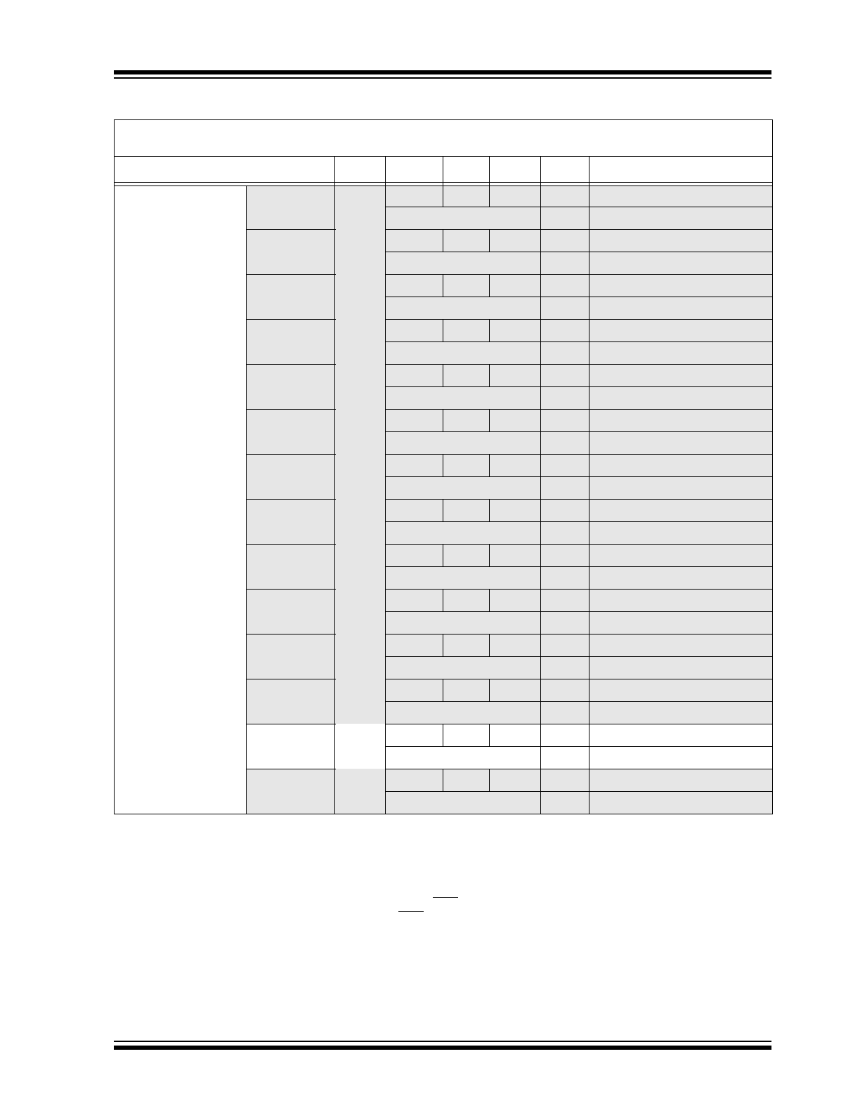
MCP131X/2X
DS21985D-page 4
2005-2012 Microchip Technology Inc.
V
DD
Trip Point
MCP13XX-20
V
TRIP
1.970
2.00
2.030
V
T
A
= +25°C (
Note 1
)
(
Note 6
)
1.950
2.00
2.050
V
T
A
= -40°C to +85°C (
Note 2
)
MCP13XX-21
2.069
2.10
2.132
V
T
A
= +25°C (
Note 1
)
(
Note 6
)
2.048
2.10
2.153
V
T
A
= -40°C to +85°C (
Note 2
)
MCP13XX-22
2.167
2.20
2.233
V
T
A
= +25°C (
Note 1
)
(
Note 6
)
2.145
2.20
2.255
V
T
A
= -40°C to +85°C (
Note 2
)
MCP13XX-23
2.266
2.30
2.335
V
T
A
= +25°C (
Note 1
)
(
Note 6
)
2.243
2.30
2.358
V
T
A
= -40°C to +85°C (
Note 2
)
MCP13XX-24
2.364
2.40
2.436
V
T
A
= +25°C (
Note 1
)
(
Note 6
)
2.340
2.40
2.460
V
T
A
= -40°C to +85°C (
Note 2
)
MCP13XX-25
2.463
2.50
2.538
V
T
A
= +25°C (
Note 1
)
(
Note 6
)
2.438
2.50
2.563
V
T
A
= -40°C to +125°C (
Note 2
)
MCP13XX-26
2.561
2.60
2.639
V
T
A
= +25°C (
Note 1
)
(
Note 6
)
2.535
2.60
2.665
V
T
A
= -40°C to +125°C (
Note 2
)
MCP13XX-27
2.660
2.70
2.741
V
T
A
= +25°C (
Note 1
)
(
Note 6
)
2.633
2.70
2.768
V
T
A
= -40°C to +125°C (
Note 2
)
MCP13XX-28
2.758
2.80
2.842
V
T
A
= +25°C (
Note 1
)
(
Note 6
)
2.730
2.80
2.870
V
T
A
= -40°C to +125°C (
Note 2
)
MCP13XX-29
2.857
2.90
2.944
V
T
A
= +25°C (
Note 1
)
2.828
2.90
2.973
V
T
A
= -40°C to +125°C (
Note 2
)
MCP13XX-30
2.955
3.00
3.045
V
T
A
= +25°C (
Note 1
)
(
Note 6
)
2.925
3.00
3.075
V
T
A
= -40°C to +125°C (
Note 2
)
MCP13XX-31
3.054
3.10
3.147
V
T
A
= +25°C (
Note 1
)
(
Note 6
)
3.023
3.10
3.178
V
T
A
= -40°C to +125°C (
Note 2
)
MCP13XX-32
3.152
3.20
3.248
V
T
A
= +25°C (
Note 1
)
(
Note 6
)
3.120
3.20
3.280
V
T
A
= -40°C to +125°C (
Note 2
)
MCP13XX-33
3.251
3.30
3.350
V
T
A
= +25°C (
Note 1
)
(
Note 6
)
3.218
3.30
3.383
V
T
A
= -40°C to +125°C (
Note 2
)
DC CHARACTERISTICS (CONTINUED)
Electrical Specifications: Unless otherwise indicated, all limits are specified for V
DD
= 1V to 5.5V, R
PU
= 100 k
(only MCP1320, MCP1321 and MCP1322), T
A
= -40°C to +125°C.
Parameters
Sym
Min
Typ
Max
Units
Conditions
Note 1:
Trip point is ±1.5% from typical value.
2:
Trip point is ±2.5% from typical value.
3:
Hysteresis is minimum = 1%, maximum = 6% at +25°C.
4:
This specification allows this device to be used in PIC
®
microcontroller applications that require the In-
Circuit Serial Programming™ (ICSP™) feature (see device-specific programming specifications for
voltage requirements). The total time that the RST pin can be above the maximum device operational
voltage (5.5V) is 100s. Current into the RST pin should be limited to 2 mA. It is recommended that the
device operational temperature be maintained between 0°C to +70°C (+25°C preferred). For additional
information, refer to
Figure 2-35
.
5:
This parameter is established by characterization and is not 100% tested.
6:
Custom ordered voltage trip point; minimum order volume requirement. Information available upon request.
2005-2012 Microchip Technology Inc.
DS21985D-page 5
MCP131X/2X
V
DD
Trip Point (Con’t)
MCP13XX-34
V
TRIP
3.349
3.40
3.451
V
T
A
= +25°C (
Note 1
)
(
Note 6
)
3.315
3.40
3.385
V
T
A
= -40°C to +125°C (
Note 2
)
MCP13XX-35
3.448
3.50
3.553
V
T
A
= +25°C (
Note 1
)
(
Note 6
)
3.413
3.50
3.588
V
T
A
= -40°C to +125°C (
Note 2
)
MCP13XX-36
3.546
3.60
3.654
V
T
A
= +25°C (
Note 1
)
(
Note 6
)
3.510
3.60
3.690
V
T
A
= -40°C to +125°C (
Note 2
)
MCP13XX-37
3.645
3.70
3.756
V
T
A
= +25°C (
Note 1
)
(
Note 6
)
3.608
3.70
3.793
V
T
A
= -40°C to +125°C (
Note 2
)
MCP13XX-38
3.743
3.80
3.857
V
T
A
= +25°C (
Note 1
)
(
Note 6
)
3.705
3.80
3.895
V
T
A
= -40°C to +125°C (
Note 2
)
MCP13XX-39
3.842
3.90
3.959
V
T
A
= +25°C (
Note 1
)
(
Note 6
)
3.803
3.90
3.998
V
T
A
= -40°C to +125°C (
Note 2
)
MCP13XX-40
3.940
4.00
4.060
V
T
A
= +25°C (
Note 1
)
(
Note 6
)
3.900
4.00
4.100
V
T
A
= -40°C to +125°C (
Note 2
)
MCP13XX-41
4.039
4.10
4.162
V
T
A
= +25°C (
Note 1
)
(
Note 6
)
3.998
4.10
4.203
V
T
A
= -40°C to +125°C (
Note 2
)
MCP13XX-42
4.137
4.20
4.263
V
T
A
= +25°C (
Note 1
)
(
Note 6
)
4.095
4.20
4.305
V
T
A
= -40°C to +125°C (
Note 2
)
MCP13XX-43
4.236
4.30
4.365
V
T
A
= +25°C (
Note 1
)
(
Note 6
)
4.193
4.30
4.408
V
T
A
= -40°C to +125°C (
Note 2
)
MCP13XX-44
4.334
4.40
4.466
V
T
A
= +25°C (
Note 1
)
(
Note 6
)
4.290
4.40
4.510
V
T
A
= -40°C to +125°C (
Note 2
)
MCP13XX-45
4.433
4.50
4.568
V
T
A
= +25°C (
Note 1
)
(
Note 6
)
4.388
4.50
4.613
V
T
A
= -40°C to +125°C (
Note 2
)
MCP13XX-46
4.531
4.60
4.669
V
T
A
= +25°C (
Note 1
)
4.485
4.60
4.715
V
T
A
= -40°C to +125°C (
Note 2
)
MCP13XX-47
4.630
4.70
4.771
V
T
A
= +25°C (
Note 1
)
(
Note 6
)
4.583
4.70
4.818
V
T
A
= -40°C to +125°C (
Note 2
)
V
DD
Trip Point Tempco
T
TPCO
—
±40
—
ppm/°C
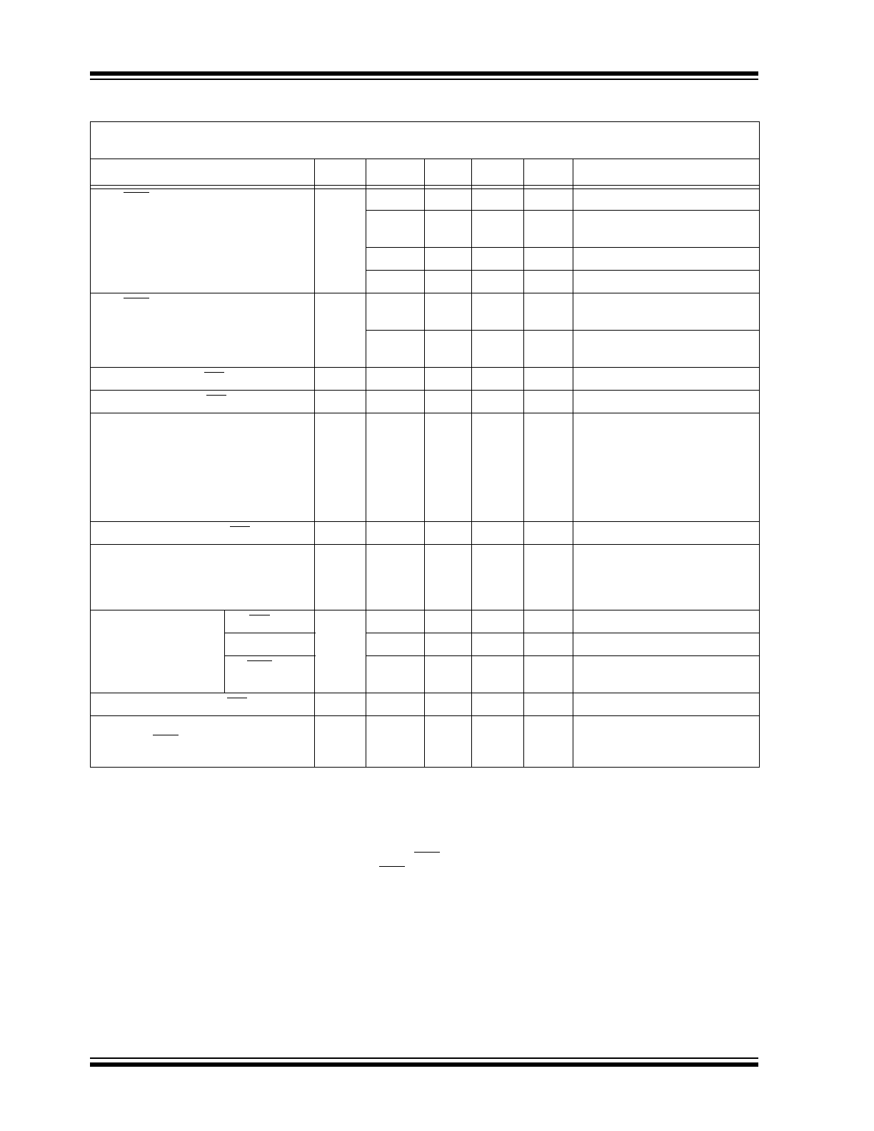
DC CHARACTERISTICS (CONTINUED)
Electrical Specifications: Unless otherwise indicated, all limits are specified for V
DD
= 1V to 5.5V, R
PU
= 100 k
(only MCP1320, MCP1321 and MCP1322), T
A
= -40°C to +125°C.
Parameters
Sym
Min
Typ
Max
Units
Conditions
Note 1:
Trip point is ±1.5% from typical value.
2:
Trip point is ±2.5% from typical value.
3:
Hysteresis is minimum = 1%, maximum = 6% at +25°C.
4:
This specification allows this device to be used in PIC
®
microcontroller applications that require the In-
Circuit Serial Programming™ (ICSP™) feature (see device-specific programming specifications for
voltage requirements). The total time that the RST pin can be above the maximum device operational
voltage (5.5V) is 100s. Current into the RST pin should be limited to 2 mA. It is recommended that the
device operational temperature be maintained between 0°C to +70°C (+25°C preferred). For additional
information, refer to
Figure 2-35
.
5:
This parameter is established by characterization and is not 100% tested.
6:
Custom ordered voltage trip point; minimum order volume requirement. Information available upon request.
MCP131X/2X
DS21985D-page 6
2005-2012 Microchip Technology Inc.
Threshold Hysteresis
MCP13XX-20
V
HYS
0.020
—
0.120
V
T
A
= +25°C (
Note 3
)
Note 3
)
(
Note 6
)
(
Note 6
)
V
T
A
= -40°C to +85°C
MCP13XX-21
0.021
—
0.126
V
T
A
= +25°C (
Note 3
)
(
Note 6
)
(
Note 6
)
V
T
A
= -40°C to +85°C
MCP13XX-22
0.022
—
0.132
V
T
A
= +25°C (
Note 3
)
(
Note 6
)
(
Note 6
)
V
T
A
= -40°C to +85°C
MCP13XX-23
0.023
—
0.138
V
T
A
= +25°C (
Note 3
)
(
Note 6
)
(
Note 6
)
V
T
A
= -40°C to +85°C
MCP13XX-24
0.024
—
0.144
V
T
A
= +25°C (
Note 3
)
(
Note 6
)
(
Note 6
)
V
T
A
= -40°C to +85°C
MCP13XX-25
0.025
—
0.150
V
T
A
= +25°C (
Note 3
)
(
Note 6
)
(
Note 6
)
V
T
A
= -40°C to +125°C
MCP13XX-26
0.026
—
0.156
V
T
A
= +25°C (
Note 3
)
(
Note 6
)
(
Note 6
)
V
T
A
= -40°C to +125°C
MCP13XX-27
0.027
—
0.162
V
T
A
= +25°C (
Note 3
)
(
Note 6
)
(
Note 6
)
V
T
A
= -40°C to +125°C
MCP13XX-28
0.028
—
0.168
V
T
A
= +25°C (
Note 3
)
(
Note 6
)
(
Note 6
)
V
T
A
= -40°C to +125°C
MCP13XX-29
0.029
—
0.174
V
T
A
= +25°C (
Note 3
)
(
Note 6
)
V
T
A
= -40°C to +125°C
MCP13XX-30
0.030
—
0.180
V
T
A
= +25°C (
Note 3
)
(
Note 6
)
(
Note 6
)
V
T
A
= -40°C to +125°C
MCP13XX-31
0.031
—
0.186
V
T
A
= +25°C (
Note 3
)
(
Note 6
)
(
Note 6
)
V
T
A
= -40°C to +125°C
MCP13XX-32
0.032
—
0.192
V
T
A
= +25°C (
Note 3
)
(
Note 6
)
(
Note 6
)
V
T
A
= -40°C to +125°C
MCP13XX-33
0.033
—
0.198
V
T
A
= +25°C (
Note 3
)
(
Note 6
)
(
Note 6
)
V
T
A
= -40°C to +125°C
DC CHARACTERISTICS (CONTINUED)
Electrical Specifications: Unless otherwise indicated, all limits are specified for V
DD
= 1V to 5.5V, R
PU
= 100 k
(only MCP1320, MCP1321 and MCP1322), T
A
= -40°C to +125°C.
Parameters
Sym
Min
Typ
Max
Units
Conditions
Note 1:
Trip point is ±1.5% from typical value.
2:
Trip point is ±2.5% from typical value.
3:
Hysteresis is minimum = 1%, maximum = 6% at +25°C.
4:
This specification allows this device to be used in PIC
®
microcontroller applications that require the In-
Circuit Serial Programming™ (ICSP™) feature (see device-specific programming specifications for
voltage requirements). The total time that the RST pin can be above the maximum device operational
voltage (5.5V) is 100s. Current into the RST pin should be limited to 2 mA. It is recommended that the
device operational temperature be maintained between 0°C to +70°C (+25°C preferred). For additional
information, refer to
Figure 2-35
.
5:
This parameter is established by characterization and is not 100% tested.
6:
Custom ordered voltage trip point; minimum order volume requirement. Information available upon request.
2005-2012 Microchip Technology Inc.
DS21985D-page 7
MCP131X/2X
Threshold Hysteresis
MCP13XX-34
V
HYS
0.034
—
0.204
V
T
A
= +25°C (
Note 3
)
(Continued)
Note 3
)
(
Note 6
)
(
Note 6
)
V
T
A
= -40°C to +125°C
MCP13XX-35
0.035
—
0.210
V
T
A
= +25°C (
Note 3
)
(
Note 6
)
(
Note 6
)
V
T
A
= -40°C to +125°C
MCP13XX-36
0.036
—
0.216
V
T
A
= +25°C (
Note 3
)
(
Note 6
)
(
Note 6
)
V
T
A
= -40°C to +125°C
MCP13XX-37
0.037
—
0.222
V
T
A
= +25°C (
Note 3
)
(
Note 6
)
(
Note 6
)
V
T
A
= -40°C to +125°C
MCP13XX-38
0.038
—
0.228
V
T
A
= +25°C (
Note 3
)
(
Note 6
)
(
Note 6
)
V
T
A
= -40°C to +125°C
MCP13XX-39
0.039
—
0.234
V
T
A
= +25°C (
Note 1
)
(
Note 6
)
(
Note 6
)
V
T
A
= -40°C to +125°C
MCP13XX-40
0.040
—
0.240
V
T
A
= +25°C (
Note 3
)
(
Note 6
)
(
Note 6
)
V
T
A
= -40°C to +125°C
MCP13XX-41
0.041
—
0.246
V
T
A
= +25°C (
Note 3
)
(
Note 6
)
(
Note 6
)
V
T
A
= -40°C to +125°C
MCP13XX-42
0.042
—
0.252
V
T
A
= +25°C (
Note 3
)
(
Note 6
)
(
Note 6
)
V
T
A
= -40°C to +125°C
MCP13XX-43
0.043
—
0.258
V
T
A
= +25°C (
Note 3
)
(
Note 6
)
(
Note 6
)
V
T
A
= -40°C to +125°C
MCP13XX-44
0.044
—
0.264
V
T
A
= +25°C (
Note 3
)
(
Note 6
)
(
Note 6
)
V
T
A
= -40°C to +125°C
MCP13XX-45
0.045
—
0.270
V
T
A
= +25°C (
Note 3
)
(
Note 6
)
(
Note 6
)
V
T
A
= -40°C to +125°C
MCP13XX-46
0.046
—
0.276
V
T
A
= +25°C (
Note 3
)
(
Note 6
)
V
T
A
= -40°C to +125°C
MCP13XX-47
0.047
—
0.282
V
T
A
= +25°C (
Note 3
)
(
Note 6
)
(
Note 6
)
V
T
A
= -40°C to +125°C
DC CHARACTERISTICS (CONTINUED)
Electrical Specifications: Unless otherwise indicated, all limits are specified for V
DD
= 1V to 5.5V, R
PU
= 100 k
(only MCP1320, MCP1321 and MCP1322), T
A
= -40°C to +125°C.
Parameters
Sym
Min
Typ
Max
Units
Conditions
Note 1:
Trip point is ±1.5% from typical value.
2:
Trip point is ±2.5% from typical value.
3:
Hysteresis is minimum = 1%, maximum = 6% at +25°C.
4:
This specification allows this device to be used in PIC
®
microcontroller applications that require the In-
Circuit Serial Programming™ (ICSP™) feature (see device-specific programming specifications for
voltage requirements). The total time that the RST pin can be above the maximum device operational
voltage (5.5V) is 100s. Current into the RST pin should be limited to 2 mA. It is recommended that the
device operational temperature be maintained between 0°C to +70°C (+25°C preferred). For additional
information, refer to
Figure 2-35
.
5:
This parameter is established by characterization and is not 100% tested.
6:
Custom ordered voltage trip point; minimum order volume requirement. Information available upon request.
MCP131X/2X
DS21985D-page 8
2005-2012 Microchip Technology Inc.
RST/RST Low-Level Output Voltage
V
OL
—
—
0.3
V
I
OL
= 50 µA, 1.0V
V
DD
1.5V
—
—
0.3
V
I
OL
= 100 µA,
1.5V
V
DD
2.5V
—
—
0.3
V
I
OL
= 2 mA, 2.5V
V
DD
4.5V
—
—
0.3
V
I
OL
= 4 mA, V
DD
4.5V
RST/RST High-Level Output Voltage
V
OH
V
DD
–
0.7
—
—
V
I
OH
= 2.5 mA, V
DD
2.5V
(Push-Pull Outputs only)
V
DD
–
0.7
—
—
V
I
OH
= 500 µA, V
DD
1.5V
Input Low Voltage (MR and WDI pins)
V
IL
V
SS
—
0.3V
DD
V
Input High Voltage (MR and WDI pins)
V
IH
0.7
V
DD
—
V
DD
V
Open-Drain High Voltage on Output
(
Note 4
)
V
ODH
—
—
13.5
(4)
V
Open-Drain Output pin only,
V
DD
= 3.0V, Time voltage >
5.5V applied
100 s,
current into pin limited to 2 mA,
+25°C operation
recommended
(
Note 4
,
Note 5
)
Input Leakage Current (MR and WDI)
I
IL
—
—
±1
µA
V
SS
V
PIN
V
DD
Open-Drain Output Leakage Current
(MCP1316M, MCP1318M,
MCP1319M, MCP1320, MCP1321,
and MCP1322 only)
I
OD
—
0.003
1.0
µA
Pull-up Resistance
MR pin
R
PU
—
52
—
k
V
DD
= 5.5V
WDI pin
—
52
—
k
V
DD
= 5.5V
RST pin
—
4.7
—
k
V
DD
= 5.5V,
MCP131XM devices only
Input Pin Capacitance (MR and WDI)
C
I
—
100
—
pF
Output Pin Capacitive Loading
(RST and RST)
C
O
—
—
50
pF
This is the tester loading to
meet the AC timing
specifications.
DC CHARACTERISTICS (CONTINUED)
Electrical Specifications: Unless otherwise indicated, all limits are specified for V
DD
= 1V to 5.5V, R
PU
= 100 k
(only MCP1320, MCP1321 and MCP1322), T
A
= -40°C to +125°C.
Parameters
Sym
Min
Typ
Max
Units
Conditions
Note 1:
Trip point is ±1.5% from typical value.
2:
Trip point is ±2.5% from typical value.
3:
Hysteresis is minimum = 1%, maximum = 6% at +25°C.
4:
This specification allows this device to be used in PIC
®
microcontroller applications that require the In-
Circuit Serial Programming™ (ICSP™) feature (see device-specific programming specifications for
voltage requirements). The total time that the RST pin can be above the maximum device operational
voltage (5.5V) is 100s. Current into the RST pin should be limited to 2 mA. It is recommended that the
device operational temperature be maintained between 0°C to +70°C (+25°C preferred). For additional
information, refer to
Figure 2-35
.
5:
This parameter is established by characterization and is not 100% tested.
6:
Custom ordered voltage trip point; minimum order volume requirement. Information available upon request.
2005-2012 Microchip Technology Inc.
DS21985D-page 9
MCP131X/2X
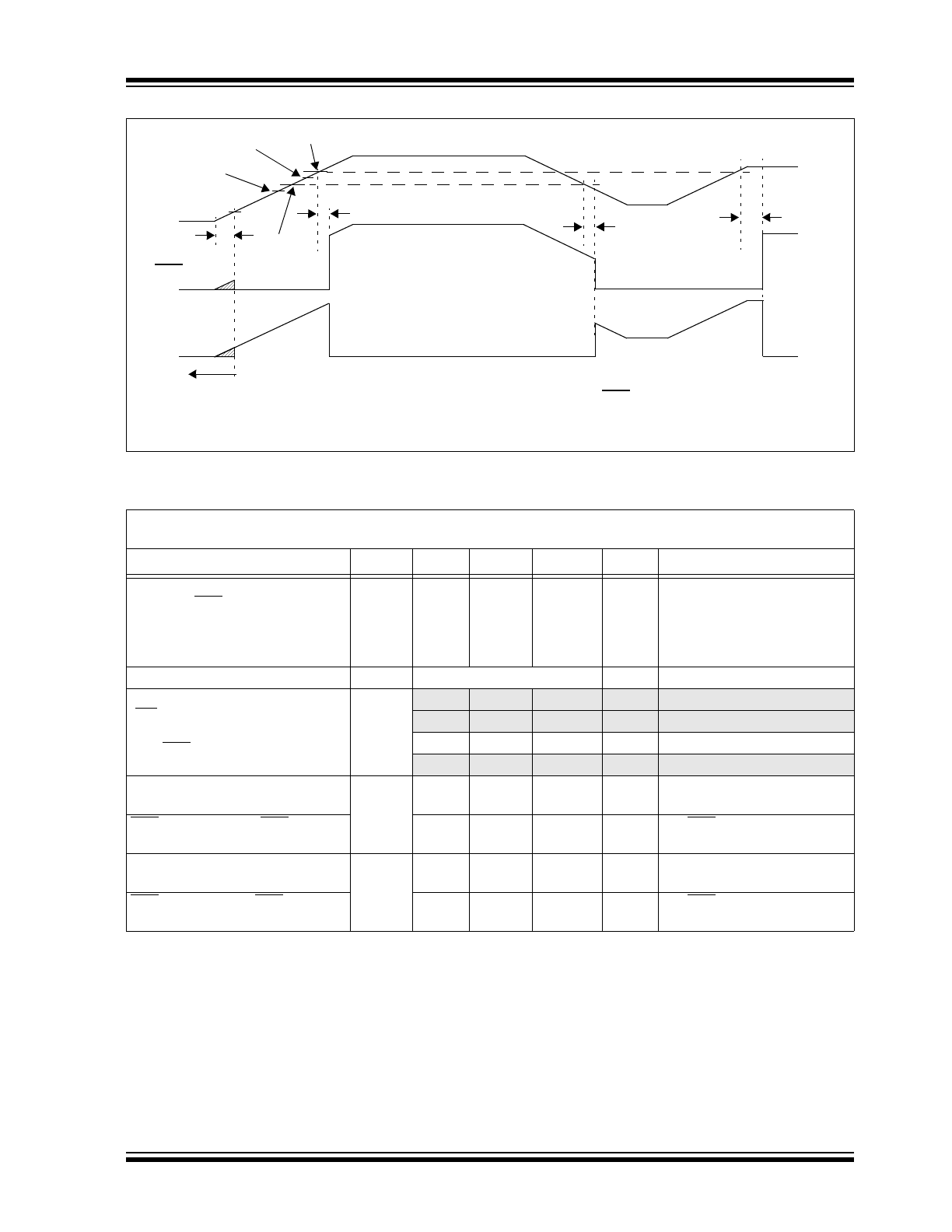
FIGURE 1-1:
Device Voltage and Reset Pin Waveforms.
TABLE 1-1:
DEVICE VOLTAGE AND RESET PIN TIMINGS
Electrical Specifications: Unless otherwise indicated, all limits are specified for V
DD
= 1V to 5.5V, R
PU
= 100 k
(only MCP1320, MCP1321, and MCP1322), T
A
= -40°C to +125°C.
Parameters
Sym
Min
Typ
Max
Units
Conditions
Falling V
DD
Trip Point Detected
to RST or RST Active
t
RPD
—
650
—
µs
V
DD
ramped from
V
TRIPMAX
+ 250 mV down to
V
TRIPMIN
– 200 mV,
V
DD
falling @ 5 mV/µs,
C
L
= 50 pF (
Note 1
)
V
DD
Rise Rate
t
RR
Note 3
Reset active time
(MR Rising Edge, POR/BOR
Inactive, or WDT time out) to
RST/RST Inactive
t
RST
1.0
1.4
2.0
ms
Note 2
20
30
40
ms
Note 2
140
200
280
ms
Standard Time Out
1120
1600
2240
ms
Note 2
RST Rise Time after RST
Active
(Push-Pull Outputs only)
t
RT
—
5
—
µs
For RST 10% to 90% of V
DD
,
C
L
= 50 pF (
Note 1
)
RST Rise Time after RST
Inactive
(Push-Pull Outputs only)
—
5
—
µs
For RST 10% to 90% of V
DD
,
C
L
= 50 pF (
Note 1
)
RST Fall Time after RST
Inactive t
FT
—
5
—
µs
For RST 90% to 10% of V
DD
,
C
L
= 50 pF (
Note 1
)
RST Fall Time after RST
Active —
5
—
µs
For
RST 90% to 10% of V
DD
,
C
L
= 50 pF (
Note 1
)
Note 1:
These parameters are for design guidance only and are not 100% tested.
2:
Custom ordered Reset active time; minimum order volume requirement.
3:
Designed to be independent of V
DD
rise rate. Device characterization was done with a rise rate as slow as
0.1 V/s (@ +25°C).
V
TRIPMAX
V
TRIPMIN
V
TRIP
1V
V
DD
V
TRIPAC
+ V
HYS
t
RST
RST
RST
t
RR
t
RST
t
RPD
V
DD
< 1V is outside the device operating specification. The RST (or RST) output state is
unknown while V
DD
< 1V.
MCP131X/2X
DS21985D-page 10
2005-2012 Microchip Technology Inc.
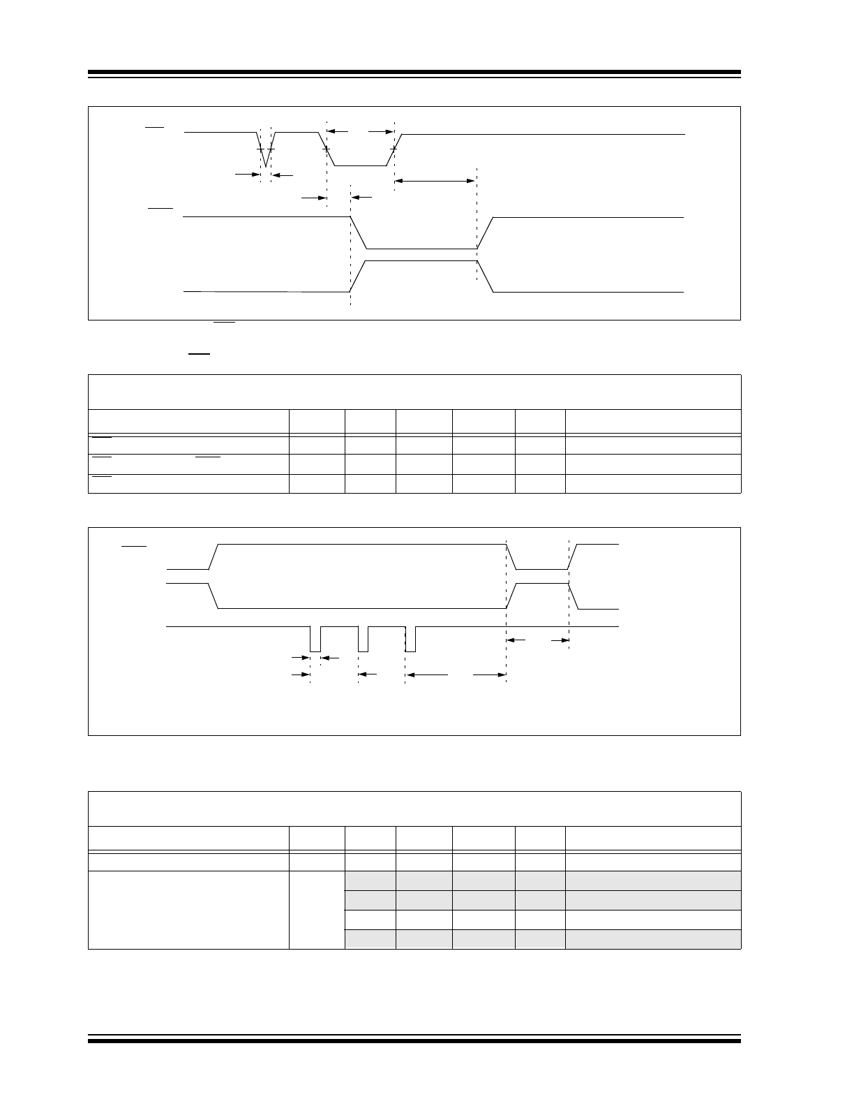
FIGURE 1-2:
MR and Reset Pin Waveforms.
TABLE 1-2:
MR AND RESET PIN TIMINGS
FIGURE 1-3:
WDI and Reset Pin Waveforms.
TABLE 1-3:
WDI AND RESET PIN TIMINGS
Electrical Specifications: Unless otherwise indicated, all limits are specified for V
DD
= 1V to 5.5V, R
PU
= 100 k
(only MCP1320, MCP1321, and MCP1322), T
A
= -40°C to +125°C.
Parameters
Sym
Min
Typ
Max
Units
Conditions
MR Pulse Width
t
MR
1
—
—
µs
MR Active to RST/RST Active
t
MRD
—
235
—
ns
V
DD
= 5.0V
MR Input Noise filter
t
NF
—
150
—
ns
V
DD
= 5.0V
Note 1:
These parameters are for design guidance only and are not 100% tested.
Electrical Specifications: Unless otherwise indicated, all limits are specified for V
DD
= 1V to 5.5V, R
PU
= 100 k
(only MCP1320, MCP1321, and MCP1322), T
A
= -40°C to +125°C.
Parameters
Sym
Min
Typ
Max
Units
Conditions
WDI Pulse Width
t
WP
50
—
—
ns
Watchdog Time-Out Period
t
WD
4.3
6.3
9.3
ms
Note 1
71
102
153
ms
Note 1
1.12
1.6
2.4
sec
Standard Time Out
17.9
25.6
38.4
sec
Note 1
Note 1:
Custom ordered WatchDog Timer time out; minimum order volume requirement.
MR
RST
t
RST
t
MR
RST
t
MRD
t
NF
RST
RST
WDI (
Note 1
)
t
WP
t
WD
t
WD
t
RST
Note 1: The WDI pin was a weak pull-up resistor which is disabled after the 1st falling edge on the WDI pin.